DEMOAC MCF51AC256 Installation manual

DOC-0440-010, RED
Web Site: www.axman.com
Support: [email protected]
DEMOAC
Development Board for Freescale FLEXIS AC MCU Family
Supports:
MCF51AC256
MC9S08AC128
MC9S08AC60
MC9S08AC16
Hardware User Guide

DEMOAC USER GUIDE APRIL 10, 2008
2
CONTENTS
CAUTIONARY NOTES ..............................................................................................................4
TERMINOLOGY.........................................................................................................................4
FEATURES ................................................................................................................................5
REFERENCES ...........................................................................................................................6
GETTING STARTED..................................................................................................................6
APPLICATION DEVELOPMENT ...............................................................................................6
HARDWARE CONFIGURATION ...............................................................................................6
INTEGRATED BDM............................................................................................................... 6
BDM PORT CONNECTOR ............................................................................................... 7
POWER................................................................................................................................. 7
EXTERNAL POWER......................................................................................................... 7
BDM POWER.................................................................................................................... 8
POWER SWITCH – PWRSW............................................................................................ 8
VOLTAGE INDICATORS .................................................................................................. 8
PWR_SEL OPTION HEADER........................................................................................... 8
VX_EN OPTION HEADER................................................................................................ 9
MCU POWER........................................................................................................................ 9
MCUVDD......................................................................................................................... 10
VDDAD............................................................................................................................ 10
VSSAD............................................................................................................................ 10
VREFH............................................................................................................................ 10
VREFL............................................................................................................................. 10
RESET SWITCH ................................................................................................................. 11
RESET LED .................................................................................................................... 11
LOW VOLTAGE DETECT............................................................................................... 11
MEMORY ............................................................................................................................ 11
TIMING................................................................................................................................ 11
COMMUNICATIONS ........................................................................................................... 12
VIRTUAL COM PORT..................................................................................................... 12
COM_EN......................................................................................................................... 12
CAN PORT...................................................................................................................... 12
IIC PORT......................................................................................................................... 12
POTENTIOMETER.............................................................................................................. 13
USER PUSHBUTTON SWITCHES ..................................................................................... 13
USER LED’S ....................................................................................................................... 13
ACCELEROMETER .................................................................................................................13
ACCELEROMETER CONFIGURATION ............................................................................. 14
MCU_PORT ........................................................................................................................15
TROUBLESHOOTING..............................................................................................................16

DEMOAC USER GUIDE APRIL 10, 2008
3
INITIAL FLASH PROGRAMMING................................................................................... 16
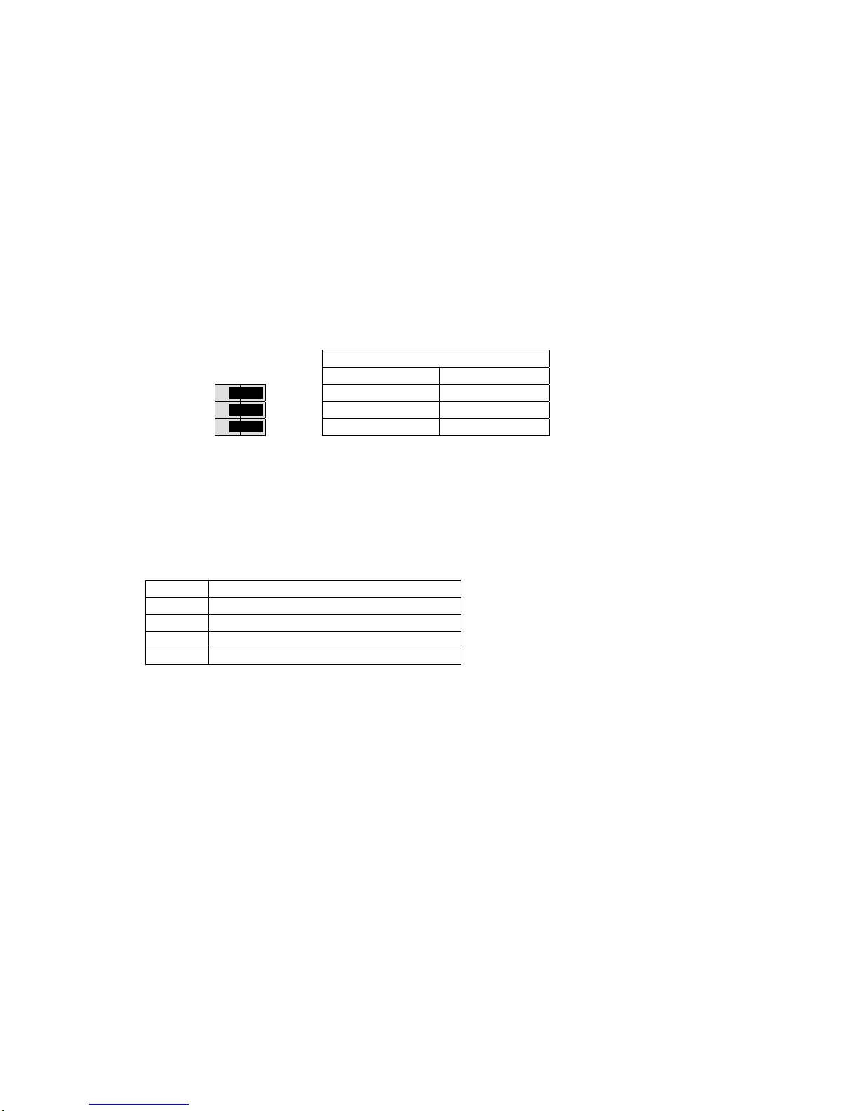
FIGURES
Figure 1: BDM Connector ...........................................................................................................7
Figure 2: PWR Jack....................................................................................................................8
Figure 3: PWR_SEL Option Header ...........................................................................................9
Figure 4: VX_EN Option Header ................................................................................................9
Figure 5: USB_COM Option Header ........................................................................................12
Figure 6: Accelerometer Sensitivity Select Header...................................................................14
Figure 7: MCU_PORT Connector.............................................................................................15
TABLES
Table 1: OSC_SEL Option Header...........................................................................................11
Table 2: POT ............................................................................................................................13
Table 3: Push Button Switches.................................................................................................13
Table 4: User LED’s..................................................................................................................13
Table 5: ACC_OUT Option Header ..........................................................................................14
REVISION
Date Rev Comments
March 20, 2008 A Initial Release.
March 29, 2008 B Minor text corrections
April 3, 2008 C Remove references to 51JM128 MCU
April 10, 2008 D Updated Troubleshooting section to account for
power-cycling board when powered from USB BDM

DEMOAC USER GUIDE APRIL 10, 2008
4
CAUTIONARY NOTES
1) Electrostatic Discharge (ESD) prevention measures should be used when handling this
product. ESD damage is not a warranty repair item.
2) Axiom Manufacturing does not assume any liability arising out of the application or use of
any product or circuit described herein; neither does it convey any license under patent
rights or the rights of others.
3) EMC Information on the DEMOAC board:
a) This product, as shipped from the factory with associated power supplies and cables,
has been verified to meet with FCC requirements as a CLASS Aproduct.
b) This product is designed and intended for use as a development platform for hardware
or software in an educational or professional laboratory.
c) In a domestic environment, this product may cause radio interference in which case the
user may be required to take adequate prevention measures.
d) Attaching additional wiring to this product or modifying the product operation from the
factory default as shipped may effect its performance and cause interference with other
apparatus in the immediate vicinity. If such interference is detected, suitable mitigating
measures should be taken.
TERMINOLOGY
This development board applies option selection jumpers. Terminology for application of the
option jumpers is as follows:
Jumper on, in, or installed = jumper is a plastic shunt that fits across 2 pins and the shunt is
installed so that the 2 pins are connected with the shunt.
Jumper off, out, or idle = jumper or shunt is installed so that only 1 pin holds the shunt, no 2
pins are connected, or jumper is removed. It is recommended that the jumpers be placed
idle by installing on 1 pin so they will not be lost.
Cut-Trace – a circuit trace connection between component pads. The circuit trace may be
cut using a knife to break the default connection. To reconnect the circuit, simply install a
suitably sized 0-ohm resistor or attach a wire across the pads.
Signal names followed by an asterisk (*) denote active-low signals.

DEMOAC USER GUIDE APRIL 10, 2008
5
FEATURES
The DEMOAC provides a platform supporting a line of Freescale microcontrollers which are
part of the Flexis Continuum. Target microcontrollers mount on plug-in modules to support
quickly changing the target MCU. Available microcontrollers for the DEMOAC include; the
ColdFire V1 MCF51AC256, and the MC9S08AC128/60/16. Application development on the
DEMOAC is quick and easy with the integrated USB-BDM, sample software tools, and exam-
ples. An optional BDM_PORT port is also provided to allow use of an external BDM cable. An
80-pin MCU_PORT connector provides access to all IO signals on the target MCU. An ex-
panded feature set, including an E-Field sensor, is provided on the DEMOACEX board. The
DEMOACEX connects to the DEMOAC through the 80-pin MCU_PORT connector.
MCU Modules:
•MCF51AC256, 80LQFP
•256K bytes FLASH
•32K bytes RAM
•ColdFire V1 Core
•50.3 MHz bus
•MC9S08AC128/60/16
•128K/60K/16K bytes FLASH
•8K/2K/1K bytes RAM
•HCS08 Core
DEMOAC Features:
•Integrated, USB BDM
•ON/OFF Power Switch
•Power Input Select Option Header
•On-board 5V regulator
•Power from USB BDM
•Optional Power Sourced to
Connector J1
•4MHz XTAL Oscillator
•3-axis accelerometer
•LEDs – 4 User, 1 Power, 1 Reset
•Push button switches – 4 user, 1 Reset
•5K ohm POT
•Jumpers to disconnect User Features
•80-pin MCU PORT provides access to MCU signals
•4 20-pos pin-headers support plug-in MCU modules
•IIC Termination Select Header
DEMOAC Board Size: 5.0” x 4.0

DEMOAC USER GUIDE APRIL 10, 2008
6
REFERENCES
The following documents should be referenced during application development using the
DEMOAC. These documents are available on the MCF51JM128 and DEMOAC web pages
(http://www.freescale.com/coldfire).
DEMOAC_UG.pdf DEMOAC User Guide (this document)
DEMOAC_QSG.pdf DEMOAC Quick Start Guide
DEMOAC_SCH_A1.pdf DEMOAC Schematic
DEMOAC_Silk_A.pdf DEMOAC Top Silk
GETTING STARTED
To get started quickly, please refer to the DEMOAC Quick Start Guide. This quick start will il-
lustrate connecting the board to a PC, installing the correct version of CodeWarrior Develop-
ment Studio, and running a simple program.
APPLICATION DEVELOPMENT
CodeWarrior Development Studio for Microcontrollers, Special Edition is provided along with
the DEMOAC to support application development and debug. CodeWarrior provides an IDE
for application debug and an integrated FLASH programmer to load application code. Refer to
the CodeWarrior Development Studio User Guide further details.
HARDWARE CONFIGURATION
The DEMOAC board provides a development or evaluation platform for a line of AC Flexis mi-
crocontrollers; including the MCF52AC256, MC9S08AC128, MC9S08AC60, and
MC9S08AC16 MCU’s. Following are descriptions of the components and options provided on
the board.
Integrated BDM
The DEMOAC board features an integrated USB BDM debugger. The integrated debugger
supports application development and debugging via the background debug mode. A type B,
USB connector provides connectivity between the target board and the host PC.
NOTE: Using the integrated USB BDM requires CodeWarrior Development Studio for Micro-
controllers Special Edition, V6.0 or later. Development tools from P&E Microcomputer
Systems also support the target device.

DEMOAC USER GUIDE APRIL 10, 2008
7
The integrated debugger provides power and ground to the target, thereby eliminating the
need to power the board externally. Power from the integrated USB BDM is derived from the
USB bus; therefore, current consumption is limited by the USB specification. Total current
consumption for the target board, and any connected circuitry, must not exceed 350 mA. Ex-
cessive current drain will violate the USB specification causing the bus to disconnect. This will
force a target POR.
CAUTION: Violating the USB specification will cause the USB bus to disconnect forcing the
target to reset. Damage to the board or host PC may result.
The integrated USB BDM provides a virtual COM port for serial communication applications.
The BMD also provides virtual instrument analyzer function. Refer to the P&E Micro Demo
Toolkit for details.
BDM Port Connector
As standard 6-pin BDM connector is also provide to allow use of external BDM cables capable
of supporting the MCF51AC26 or MC9S08AC128/60/16 devices.
Figure 1: BDM Connector
BKGD*/MS 1 2 VSS
3 4 RESET*
5 6 VDD
POWER
The DEMOAC may be powered from the integrated USB BDM, an on-board voltage regulator,
or from the MCU connector at J1. Alternatively, the DEMOAC may be configured to provide
power to external circuitry connected to the MCU connect J1.
The PWRSW power switch controls input voltage to the board regardless of input voltage
source.
External Power
The power jack at POWER allows the board to be powered from an externally connected
power source. This connection accepts a standard 2.1mm, center-positive, barrel plug con-
nector. +VIN should fall between +7VDC and +18VDC. Input voltage applied to the barrel
connector should be kept as lows as possible to minimize device heating.

DEMOAC USER GUIDE APRIL 10, 2008
8
Figure 2: PWR Jack
2.1mm, center-positive, +V input
Applied voltage: +7V to +18V
PWR
A voltage regulator provides +5V to the target MCU and board circuitry. The regulator pro-
vides a maximum of 500 mA. The regulator is over-current and over-temperature protected to
prevent damage during fault conditions.
BDM Power
The integrated USB BDM is configured to provide power to the target device and connected
circuitry. After the BDM enumerates on the USB bus, the BDM will provide up to 350 mA to
the board. Excessive current drain will violate the USB specification and cause de-enumerate
the BDM. This will disconnect power to the board and cause a target reset.
CAUTION: Violating the USB specification will cause the USB bus to disconnect forcing the
target to reset. Damage to the board or host PC may result.
Power Switch – PWRSW
The PWRSW easily connects and disconnects input voltage to the board. The silkscreen
clearly marks the ON and OFF positions. This switch controls all voltage levels on the board.
Voltage Indicators
A +5V LED indicates the board is powered.
PWR_SEL Option Header
The PWR_SEL option header selects the source of input power to the EVB. The board may
be powered from a voltage source connected to either the POWER connector or the integrated
USB BDM. The BDM can provide up to 350 mA of current to the EVB.

DEMOAC USER GUIDE APRIL 10, 2008
9
Figure 3: PWR_SEL Option Header
PWR_SEL
• • • Selects input voltage from POWER connector
BDM VR1 NOTE: The VR1 input is connected to the regulator at VR2.
This is an error in the board silkscreen.
PWR_SEL
• • • Selects input voltage from the integrated BDM
BDM VR1
NOTE: The voltage regulator reference designator at the PWR_SEL option header does not
match the reference designator of the voltage regulator.
VX_EN Option Header
The VX_EN option header is a 2-pin jumper that connects the target-board voltage rail to IO
connector position J1-1. IO connector position J1-3 connects directly to the ground plane.
This input requires a regulated +5.0V voltage source. This power input is decoupled to mini-
mize noise input but is not regulated. Also, no protection is applied on this input and damage
to the target board may result if over-driven. Do not attempt to power the target board through
this connector while also applying power through the PWR connector as damage to the board
may result.
Power may be sourced to off-board circuitry through the MCU_PORT. The current limitation of
the on-board regulator must be considered when attempting to source power to external cir-
cuitry. Excessive current drain may damage the target board or the on-board regulator. The
figure below shows the VX_EN option header connections.
Figure 4: VX_EN Option Header
ON Enable power connection to connector J1
VX_EN
▪ ▪ OFF Disable power connection to connector J1
VX_EN
CAUTION: Do not apply power to connector J1 while also sourcing power from either the
PWR connector. Damage to the board may result.
NOTE: Do not exceed available current supply from on-board regulator when sourcing power
through connector J1 to external circuitry.
MCU Power
Each power input is routed through an option header. The option header is not installed in
default configurations and a cut-trace on each power input provides default connections. To

DEMOAC USER GUIDE APRIL 10, 2008
10
apply an alternate power input, simply remove the cut-trace using a sharp knife. Then either
solder a wire to the thru-hole via or install a pin header and wire-wrap a wire connection.
The various power inputs are grouped together at JP1. This allows each voltage input to be
selected individually using multiple 1x2 pin headers or all voltage input may be selected using
a 2x5 pin header.
MCUVDD
The VDD option header applies board VDD to the target MCU. This jumper may be used to
apply alternate voltage levels or to measure input current under operating conditions.
VDDAD
The VDDA option header connects the target device VDDA input to the VDD rail by default.
This jumper may be used to apply alternate voltage input or to measure input current under
operating conditions.
VSSAD
The VSSA option header connects the target device VSSA input to the EVB digital ground rail
by default. This option header may be used to apply ultra clean ground or to measure input
current under operating conditions.
VREFH
The VREFH option header connects the target device VREFH input to the VDD rail by default.
This jumper may be used to apply alternate voltage input or to measure input current under
operating conditions.
VREFL
The VREFL option header connects the target device VREFL input to the ground rail by de-
fault. This option header may be used to apply ultra clean ground or to measure input current
under operating conditions.

DEMOAC USER GUIDE APRIL 10, 2008
11
RESET Switch
The RESET switch allow the manual application of the RESET* signal. Application of RESET
halts the current operation and initializes internal registers to their default state. The previous
operating state of the target device will be lost.
External reset may also be applied directly to the RESET * signal at connector J1A-4.
Reset LED
The RESET indicator will be ON for the duration of a valid RESET* signal. The RESET * sig-
nal is driven active while the MCU is in the RESET state.
Low Voltage Detect
The different AC MCU’s apply a Low Voltage Detect (LVD) module to detect under-voltage
conditions. The LVD may be configured to generate a RESET or an interrupt. Refer to the
target device Reference Manual for further details.
MEMORY
No external memory is applied to the DEMOAC board. Memory for application development is
internal to the target MCU. Refer to the target device Reference Manual for further details.
TIMING
The DEMOAC board provide a 4Mhz oscillator timing source for use with the target MCU. The
OSC_SEL option header allows this input to be disconnected if necessary. In default configu-
rations, the OSC_SEL option header is not installed and cut-traces provide the default connec-
tions.
To either disconnect the oscillator input or to apply an alternate frequency, remove the cut-
traces. To restore the default connection, install a 2x2 pin header and 2 shunts.
Table 1: OSC_SEL Option Header
●●EXTAL Oscillator or External Clock Input w/ cut-trace in default configurations
●●XTAL Oscillator Input w/ cut-trace in default configurations
CAUTION: Communications with the target may be lost if clock frequency or baud rate
changes during application execution.

DEMOAC USER GUIDE APRIL 10, 2008
12
Communications
The DEMOAC board provides 2 UART ports, 1 IIC port, and 1 CAN port. Serial RS-232 com-
munications is support through the integrated BDM. Access to each MCU UART is also avail-
able at connector J1. RS-232 translation is not provided on signals to connector J1.
Virtual COM Port
The serial link through the integrated USB BDM is implemented as a virtual COM port running
through the USB connection. Use of this link require installation of the P&E Micro Demo Board
Toolkit. This toolkit is available on the DVD provided with the DEMOAC.
Refer to the P&E documentation for details and instructions on use of the virtual COM port.
COM_EN
The USB_COM option header individually connects and disconnects the target UART signals
to the integrated USB BDM. Removing a shunt disconnects the associated signal. Installing a
shunt connects the associated signal.
Figure 5: USB_COM Option Header
Shunt
On Off
▪ ▪ RXD Enabled (*) Disabled
▪ ▪ TXD Enabled (*) Disabled
(*) – Default condition
NOTE: TGT_TXD and TGT_RXD connect TXD2 and RXD2 lines to the serial input of the inte-
grated BDM.
CAN Port
CAN port signals connect directly between the target MCU and the MCU Port connector at J1.
Refer to the target MCU device Reference Manual for details on using this feature.
IIC Port
IIC port signals connect directly between the target MCU and the MCU Port connector at J1.
Refer to the target MCU device Reference Manual for details on using this feature. Each IIC
signal is pulled up to VDD at the I2C_PULL_EN option header.

DEMOAC USER GUIDE APRIL 10, 2008
13
Potentiometer
A 5k ohm, single-turn, thumb-wheel type, potentiometer at RV1 provides continuous, variable
resistance input for user applications. The potentiometer is connected between VDD and GND
with the center tap providing the divider output. The center tap is connected to the MCU at :
Table 2: POT
POT PTD0/AD1P8/ACMP1+
User Pushbutton Switches
Four user push-button switches are provided for user application input as needed and are con-
figured for active-low signaling. SW1 – SW4 are applied to keyboard interrupt inputs on the
target MCU. Use of target device internal pull-ups is required for proper operation. No external
bias is applied to any push-button switch input. Use of target device internal pull-ups is re-
quired for proper operation.
Table 3: Push Button Switches
Switch Signal
SW1 PTG0/KBI1P0
SW2 PTG1/KBI1P1
SW3 PTG2/KBI1P2
SW4 PTG3/KBI1P3
User LED’s
Eight user LED's are provided for output indication and are configured for active-low signaling.
The table below details the LED connections to the target MCU
Table 4: User LED’s
LED Signal
LED1 PTF0/RGPIO8/FTM1CH2
LED2 PTF1/RGPIO9/FTM1CH3
LED3 PTF4/RGPIO12/FTM2CH0
LED4 PTF5/RGPIO13/FTM2CH1
ACCELEROMETER
DEMOAC USER GUIDE APRIL 10, 2008
14
The DEMOAC applies the MMA7260Q, 3-axis accelerometer for tilt and motion-sense applica-
tions. The accelerometer supports 4 user selectable sensitivities - 1.5g / 2g / 4g / 6g. The
SLEEP* input allows the device to be placed in a low-power mode. Separate X-, Y-, and Z-
axis readings are routed to the MCU. The X-axis output is routed to two separate inputs on the
target MCU. Low-pass filters remove hi-frequency components on each axis output.
Accelerometer Configuration
Accelerometer sensitivity configuration is controlled manually using option select header JP2.
Figure 6: Accelerometer Sensitivity Select Header
Shunt
JP2 On Off
GSEL1 ▪ ▪ Enabled Disabled (*)
GSEL2 ▪ ▪ Enabled Disabled (*)
SLEEP* ▪ ▪ Enabled Disabled (*)
(*) – Default condition
An option header at ACC_OUT allows the user to disconnect the accelerometer output if nec-
essary. The ACC_OUT option header is not installed default configurations and cut-traces
provide default connections
Table 5: ACC_OUT Option Header
Signal MCU Input
X PTD0/ADP8/ACMP+
X PTB3/SS2*/ADP3
Y PTB0/MISO2/ADP0
Z PTB1/MOSI2/ADP1

DEMOAC USER GUIDE APRIL 10, 2008
15
MCU_PORT
The MCU PORT provides user access to the DEMOAC I/O ports. Refer to the MCF51AC256
or MC9S08AC128/60/16 Integrated Device Reference Manual for signal details.
Figure 7: MCU_PORT Connector
VDD 1 2 IRQ*/TPMCLK
VSS 3 4 RESET*
PTE0/RGPIO0/TXD1 5 6 BKGD/MS
PTE1/RGPIO1/RXD1 7 8 PTD6/FTM1CLK/AD1P14
PTG0/KBI1P0 910 VREFH
PTG1/KBI1P1 11 12 VREFL
PTE2/RGPIO2/FTM1CH0 13 14 PTD0/AD1P8/ACMP1+
PTE3/RGPIO3/FTM1CH1 15 16 PTD1/AD1P9/ACMP1-
PTE6/RGPIO6/MOSI1 17 18 PTB3/AD1P3
PTE5/RGPIO5/MISO1 19 20 PTB2/AD1P2
PTE7/RGPIO7/SPSCK1 21 22 PTB0/TPM3CH0/AD1P0
PTE4/RGPIO4/SS1* 23 24 PTB1/TPM3CH1/AD1P1
PTD2/KBI1P5/AD1P10/ACMP1O 25 26 PTA0/TXCAN
PTD3/KBI1P6/AD1P11 27 28 PTA1/RXCAN
PTG2/KBI1P2 29 30 PTH5/MOSI2
PTG3/KBI1P3/AD1P18 31 32 PTH6/MISO2
PTF0/RGPIO8/FTM1CH2 33 34 PTH4/SPSCK2
PTF1/RGPIO9/FTM1CH3 35 36 PTC4/SS2*
PTF4/RGPIO12/FTM2CH0 37 38 PTC3/TXD2
PTF5/RGPIO13/FTM2CH1 39 40 PTC5/RXD2
PTF2/RGPIO10/FTM1CH4 41 42 PTC0/SCL1
PTF3/RGPIO11/FTM1CH5 43 44 PTC1/SDA1
PTF6/RGPIO14/FTM1FLT 45 46 PTC2/MCLK
PTF7/RGPIO15 47 48 PTC6/FTM2FLT
PTB4/AD1P4 49 50 PTA2
PTB5/AD1P5 51 52 PTA3/ACMP2O
PTB6/AD1P6 53 54 PTA4/ACMP2-
PTB7/AD1P7 55 56 PTA5/ACMP2+
PTD4/FTM2CLK/AD1P12 57 58 PTA6/AD1P16
PTD5/AD1P13 59 60 PTA7/AD1P17
PTD6/FTM1CLK/AD1P14 61 62 PTG5/XTAL
PTD7/KBI1P7/AD1P15 63 64 PTG6/EXTAL
VDDAD 65 66 PTJ0/PST0
VSSAD 67 68 PTJ1/PST1
PTG4/KBI1P4/AD1P19 69 70 PTJ2/PST2
NC 71 72 PTJ3/PST3
PTH0/FTM2CH2/AD1P20 73 74 PTJ4/DDATA0
PTH1/FTM2CH3/PSTCLK0/AD1P21 75 76 PTJ5/DDATA1
PTH2/FTM2CH4/PSTCLK1/AD1P22 77 78 PTJ6/DDATA2
PTH3/FTM2CH5/BKPT/AD1P23 79 80 PTJ7/DDATA3

DEMOAC USER GUIDE APRIL 10, 2008
16
TROUBLESHOOTING
The DEMOAC is fully tested and operational before shipping. If it fails to function properly, in-
spect the board for obvious physical damage first. Verify the communications setup as de-
scribed under GETTING STARTED.
Initial Flash Programming
To program target device FLASH initially, or if device FLASH is erased, apply external power
at the PWR jack and set the PWR_SEL option header to VR1. When prompted by P&E soft-
ware to cycle target power, move the PWRSW to the OFF position momentarily then to the ON
position. Otherwise, the BDM will fail to connect to the target device.
Most common problems are related to improperly configured options or communications pa-
rameters.
1. If the simulator software requires a device power cycle during FLASH programming, en-
sure the board is powered externally and the PWR_SEL option header is set to VR1.
2. Verify the +5V voltage indicator is ON.
3. Verify input power is connected. If powered from an external power source, measure at
least +7V between VR2-1 and VR2-2 using a multi-meter. If powered from the integrated
BDM, measure +5V across capacitor C16
4. Ensure the PWRSW is in the ON position.
5. Verify default option jumper settings and RESET the board.
6. Ensure target module is securely, and correctly, seated on pin headers JM1 – JM4.
7. If a peripheral feature does not function properly, ensure all USER select jumpers are in-
stalled.
complete description of the problem.

Mouser Electronics
Authorized Distributor
Click to View Pricing, Inventory, Delivery & Lifecycle Information:
Freescale Semiconductor:
DEMO51AC256KIT DC9S08AC128 DC9S08AC16 DC9S08AC60
This manual suits for next models
3
Table of contents


