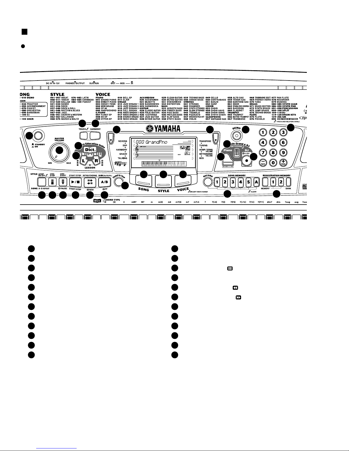
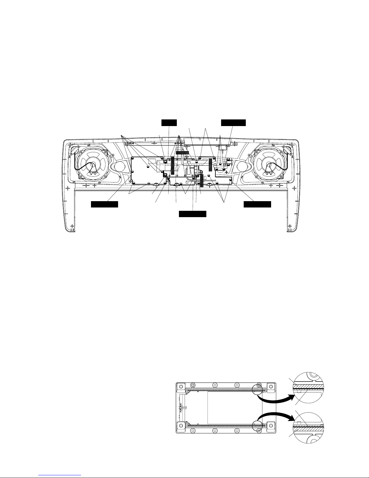
Pioneer PORTATONE PSR-280 User manual

SERVICE MANUAL
PK 001641
HAMAMATSU, JAPAN
1.43K-257 Printed in Japan '00.06
CONTENTS
SPECIFICATIONS···································································· 3
PANEL LAYOUT······································································· 4
CIRCUIT BOARD LAYOUT······················································ 6
BLOCK DIAGRAM···································································· 8
DISASSEMBLY PROCEDURE················································· 9
LSI PIN DESCRIPTION·························································· 12
IC BLOCK DIAGRAM ····························································· 14
CIRCUIT BOARDS································································· 15
TEST PROGRAM··································································· 24
DATA INITIALIZATION··························································· 26
MIDI IMPLEMENTATION CHART·········································· 27
PARTS LIST
OVERALL CIRCUIT DIAGRAM
This document is printed on chlorine free (ECF) paper with soy ink.
PSR-280
PSR-282

PSR-280/PSR-282
2
WARNING: CHEMICAL CONTENT NOTICE!
The solder used in the production of this product contains LEAD. In addition, other electrical/electronic and/or plastic (where
applicable) components may also contain traces of chemicals found by the California Health and Welfare Agency (and possibly
other entities) to cause cancer and/or birth defects or other reproductive harm.
DO NOT PLACE SOLDER, ELECTRICAL/ELECTRONIC OR PLASTIC COMPONENTS IN YOUR MOUTH FOR ANY REASON
WHAT SO EVER!
Avoid prolonged, unprotected contact between solder and your skin! When soldering, do not inhale solder fumes or expose eyes
to solder/flux vapor!
If you come in contact with solder or components located inside the enclosure of this product, wash your hands before handling
food.
IMPORTANT NOTICE
This manual has been provided for the use of authorized Yamaha Retailers and their service personnel. It has been assumed that
basic service procedures inherent to the industry, and more specifically Yamaha Products, are already known and understood by
the users, and have therefore not been restated.
WARNING: Failure to follow appropriate service and safety procedures when servicing this product may result in personal
injury, destruction of expensive components and failure of the product to perform as specified. For these
reasons, we advise all Yamaha product owners that all service required should be performed by an authorized
Yamaha Retailer or the appointed service representative.
IMPORTANT: This presentation or sale of this manual to any individual or firm does not constitute authorization, certification,
recognition of any applicable technical capabilities, or establish a principal-agent relationship of any form.
The data provided is belived to be accurate and applicable to the unit(s) indicated on the cover. The research engineering, and
service departments of Yamaha are continually striving to improve Yamaha products. Modifications are, therefore, inevitable and
changes in specification are subject to change without notice or obligation to retrofit. Should any discrepancy appear to exist,
please contact the distributor's Service Division.
WARNING: Static discharges can destroy expensive components. Discharge any static electricity your body may have
accumulated by grounding yourself to the ground bus in the unit (heavy gauge black wires connect to this bus).
IMPORTANT: Turn the unit OFF during disassembly and parts replacement. Recheck all work before you apply power to the
unit.
WARNING
Components having special characteristics are marked and must be replaced with parts having specification equal to those
originally installed.

SPECIFICATIONS
PSR-280/PSR-282
3
Keyboards
• 61 standard-size keys (C1 - C6), with Touch Response and
Dynamic Filter.
Display
• Large multi-function LCD display (backlit)
Setup
• STANDBY/ON
• MASTER VOLUME: MIN - MAX
Panel Controls
• OVERALL (L, R), SONG, VOICE, STYLE, PORTABLE
GRAND, DJ, METRONOME, [0]-[9], [+](YES), [-](NO),
DEMO, TOUCH, HARMONY, Dict., L, R, TEMPO/TAP
Voice
• 118 panel voices + 10 Drum Kits + 128 GM Voices
• Polyphony: 32
• Voice Set
Auto Accompaniment
• 100 styles
• Accompaniment Control: ACMP ON/OFF, SYNC STOP,
SYNC START, START/STOP,
INTRO/ENDING, MAIN A/B(AUTO
FILL)
• Fingering : Multi fingering
• Accompaniment Volume
Yamaha Educational Suite
• Dictionary
• Lesson 1-4
One Touch Setting
• Voice (for each style or song)
Overall controls
• Transpose
• Tuning
• Accompaniment Volume
• Song Volume
• Metronome Volume
• MIDI
• Reverb
• DSP
• Harmony
• Grade
• Talking
Effects
• Reverb: 8 types
• DSP: 37 types
• Harmony: 26 types
Song
• 100 Songs + 5 User Songs
• Song Clear, Track Clear
Recording
• Song
User Song: 5 Songs
Real Time Recording
Recording Tracks: 1, 2, 3, 4, 5, CHORD
MIDI
• Clock
• Bulk Send/Receive
• Initial Send
Auxiliary jacks
• PHONES/OUTPUT, DC IN 10-12 V, MIDI IN/OUT, SUSTAIN
Amplifier
• 3.0 W + 3.0 W
Speakers
• 12 cm x 2 + 3 cm x 2
Power Consumption
• 15 W (when using PA-3B power adaptor)
Power Supply
• Adaptor: Yamaha PA-3B AC power adaptor
• Batteries: Six “D” size, SUM-1, R-20 or equivalent batteries
Dimensions (W x D x H)
• 933 x 370 x 129 mm (36-3/4" x 14-5/8" x 5-1/6")
Weight
• 5.5 kg (12 lbs., 2 oz.)
Supplied Accessories
• Music Stand
• Owner’s Manual
• Song Book
Optional Accessories
• Headphones: HPE-150
• AC power adaptor: PA-3B
• Footswitch: FC4, FC5
• Keyboard stand: L-2L, L-2C

PSR-280/PSR-282
4
PANEL LAYOUT
1
2
3 4
5
6
7 7
10
9
8
11
12
2423
222120
19
18
1716151413
1Power switch ([STANDBY/ON])
2[MASTER VOLUME] dial
3[TOUCH] button
4[HARMONY] button
5[Dict.] (DICTIONARY) button
6LESSON [L] (Left) and [R] (Right) buttons
7Overall (left, right) buttons
8[DEMO] button
9[Piano] button
10 [METRONOME] button
11 [DJ] button
12 Numeric keypad, [+/YES] and [-/NO] buttons
13 [ACMP ON/OFF] / [A-B REPEAT] button
14 [SYNC STOP] button
15 [SYNC START] / [ PAUSE] button
16 [START/STOP] button
17 [INTRO/ENDING] / [ REW] button
18 [MAIN/AUTO FILL] / [ FF] button
19 [TEMPO/TAP] button
20 [SONG] button
21 [STYLE] button
22 [VOICE] button
23 [SONG MEMORY] buttons
24 REGISTRATION MEMORY buttons
Front Panel

25 26 27 28
29
33
343537
30
38 39 36
3140 41 32
25 MIDI IN, OUT terminals
26 SUSTAIN jack
29 Indicators
30 Overall indicator
31 Notation
32 Keyboard
33 Measure
34 Beat marks
35 Chord
27 PHONES/OUTPUT jack
28 DC IN 10-12V jack
36 Song/Voice/Style name and number, Tempo
37 Song track indicators
38 Touch indicator
39 Harmony indicator
40 Sync Stop indicator
41 Accompaniment On indicator
PSR-280/PSR-282
5
Rear Panel
Display

DM
AM
CN102
CN501CN101
390 WH100 WH050WH060WH040
WH500 380
380WH300 WH400380
WH200
WH500WH010
L70WH020
L70WH400WH300
WH040
WH050WH030
LCD unit Upper case assembly
Speaker R (Tweeter)
Speaker R (Woofer)
Speaker L (Tweeter)
Speaker L (Woofer)
Keyboard assembly
PN(PNR) PN(PNC)
LCD
PN(PNL)
PN(PW)
MK-LMK-H
MKS3
PN(VR)
CN911
CN910
CN101
CN912
CN820
CN810
CN801
CN601
CN701
CN702
CN601
CN501
CN911
CN801
CN1
CN703
CN706
CN705
CN701 CN704
2NC-V524070 3
PSR-280/PSR-282
6
CIRCUIT BOARD LAYOUT

PSR-280/PSR-282
7
PN(PNR)-CN701 DM-CN702 14PDM-PN-R
Connector AssemblyPart No.
(V539010)
Location Destination Remarks
WH010
PN(PNR)-CN703 PN(PNL)-CN704 9PPN-R-PN-L(V539100)
WH020
PN(PNL)-CN705 PN(PNC)-CN706 4PPN-L-PN-C(V539110)
WH030
PN(VR)-CN501 DM-CN501 4PDM-VR(V539030)
WH040
PN(VR)-CN801 AM-CN801 4PAM-VR(V539060)
WH050
PN(PW)-CN911 AM-CN911 4PAM-PSW(V539040)
WH060
AM-CN101 DM-CN101 5PDM-AM1(V538990)
WH100
AM-CN601 DM-CN601 6PDM-AM2(V539000)
WH200
AM-CN810 SPEAKER R 2PAM-SP-R(V539140)
WH300
SPEAKER R
AM-CN820 SPEAKER L 2PAM-SP-L(V560490)
WH400
SPEAKER L
LCD-CN1 DM-CN701 12PDM-LCD(V538980)
WH500
LCD UNIT AM-CN912 2PAM-LCD(V539120)
L70
POWER SUPPLYAM-POWER(V539130)
380
KEYBOARD ASSEMBLY
DM-MKS(V616910)
390
DM-CN102 6P
AM-CN910 2P
* Connector assembly listed above are not available as service parts.

Keyboard SW MATRIX
8MHz
RESET SWX00
4.2V
CPU
CL1 IC1
LCD
DRIVER SW MATRIX STANDBY/ON
IC701
LCD
DISPLAY
LD701
LCD
BUCKLIGHT
CN1
CN102 CN701 CN702
CN701 CN911
CN911
CN1
TXD1, LSIIC, RXD1, SCLKI PAD0~5, PDT0~7, 11, 12
C1~C16,
S1~S40
S-BUS D0~15, A0~20
C-BUS D0~15, A0~20
IC103
1
9
153 14
312 1
21
SW60
32
20
156
158, 163, 164
5~7
IC101
RXD0
TXD0
ADIN
CLOCK
DAC
8.4672MHz
CL001
DO0, WCLK, QCLK
IC501 LPF
EQ
POWER
AMP PHONES/
OUTPUT
IC502
IC800
IC810
IC820
13
1521
17
12
147
7
7
2
6
2
5
6
CN101
CN601
CN101
CN601
JK620
JK630
JK900
JK640
CN820 1
2
1
2
CN810
IC820
IC810
+
+
+
+
3W x 2
CN501
CN501
CN801CN801
MASTER
VOLUME
MIDI I/F
IC601
+3.3V REG
Tweeter L
SUSTAIN
MIDI IN
MIDI OUT
DC IN
10-12V
BATTERIES
1.5V x 6
Tweeter R
SP-L 4
SP-R 4
IC102
+5V REG
IC930
+5V REG
IC920
+5V REG
IC940
+3.3D
+5D
+5V
8M ROM
PROGRAM
IC202
1M SRAM
IC302
1M SRAM
IC301
ROM2
32M ROM
WAVE
IC201
ROM1 +5V
CN910
DM
MK
MKS3
AM
PN(PNL, PNC, PNR)
LCD PN(PW)
PN(VR) 28CA1-8816895
PSR-280/PSR-282
8
BLOCK DIAGRAM

DM AM
MKS3
PN(PW)
Keyboard assembly [A]
[240]
Lower shield box
[260B][280][250C]
[260B] [250A] [250A] [30]
[260B] [250A]
[250B][250A]
[270B]
[270B] [270B]
[250C]: Bind Head Tapping Screw-P 3.0 x 8 MFZN2Y (EP600280) [280]: Bind Head Tapping Screw-P 4.0 x 8 MFZN2BL (VB931600)
(Fig. 2)
Speaker R
(Tweeter)
Speaker R
(Woofer)
[250C] [280] [250C]
Speaker L
(Tweeter)
Speaker L
(Woofer)
[250C]
+– +–
Battery cover assembly[260A] Lower case assembly
[260A]
[260A][260A]
[270A] [270A]
[260A]
[260A]: Bind Head Tapping Screw-P 3.0 x 12 MFZN2Y (EP600300) [270A]: Bind Head Tapping Screw-P 3.0 x 25 MFZN2Y (VK228100)
(Fig. 1)
DISASSEMBLY PROCEDURE
PSR-280/PSR-282
9
1. Lower Case Assembly
1-1 Remove the battery cover assembly. (Fig. 1) 1-2 Remove the fifteen (15) screws marked [260A] and two
(2) screws marked [270A]. The lower case assembly can
then be removed. (Fig. 1)
2. Circuit Board and Units on the Panel Asseembly
After removing the lower case assembly. (See Procedure 1.)
Remove the following screws, each circuit board and can be removed. (Fig. 2)
Circuit Board and Unit
DM
AM
PN(PW)
MKS3
Keyboard Assembly
[260B]
[240]
[250A]
[250B]
[A]
[30]
[270B]
Bind Head Tapping Screw-P 3.0 x 12 MFZN2Y (EP600300)
Bind Head Tapping Screw-B 3.0 x 8 MFZN2Y (EP600250)
Bind Head Tapping Screw-P 3.0 x 8 MFZN2Y (EP600280)
Push Knob (VQ218800)
Bind Head Tapping Screw-P 3.0 x 8 MFZN2Y (EP600280)
Bind Head Tapping Screw-P 3.0 x 25 MFZN2Y (VK228100)
5
9
7
2
1
2
3
Ref. No. Screw QTY

PN(VR)LCD
PN(PNL)
PN(PNC)
PN(PNR)
[250D][L50]
[250H] [250E]
[250E]
[250E][250F] [250F]
[250H]
[250G]
[250H]
[250G]
[250G]
[250H]
LCD unit
[250]: Bind Head Tapping Screw-P 3.0 x 8 MFZN2Y (EP600280) [L50]: Bind Head Tapping Screw-P 3.0 x 8 MFZN2Y (EP600280)
(Fig. 3)
PSR-280/PSR-282
10
3. Speakers
3-1 Remove the lower case assembly. (See Procedure 1.)
3-2 Woofer:
Remove the four (4) screws marked [280]. The right and
left speakers (woofer) can then be removed. (Fig. 2)
3-3 Tweeter:
Remove the two (2) screws marked [250C]. The right and
left speakers (tweeter) can then be removed. (Fig. 2)
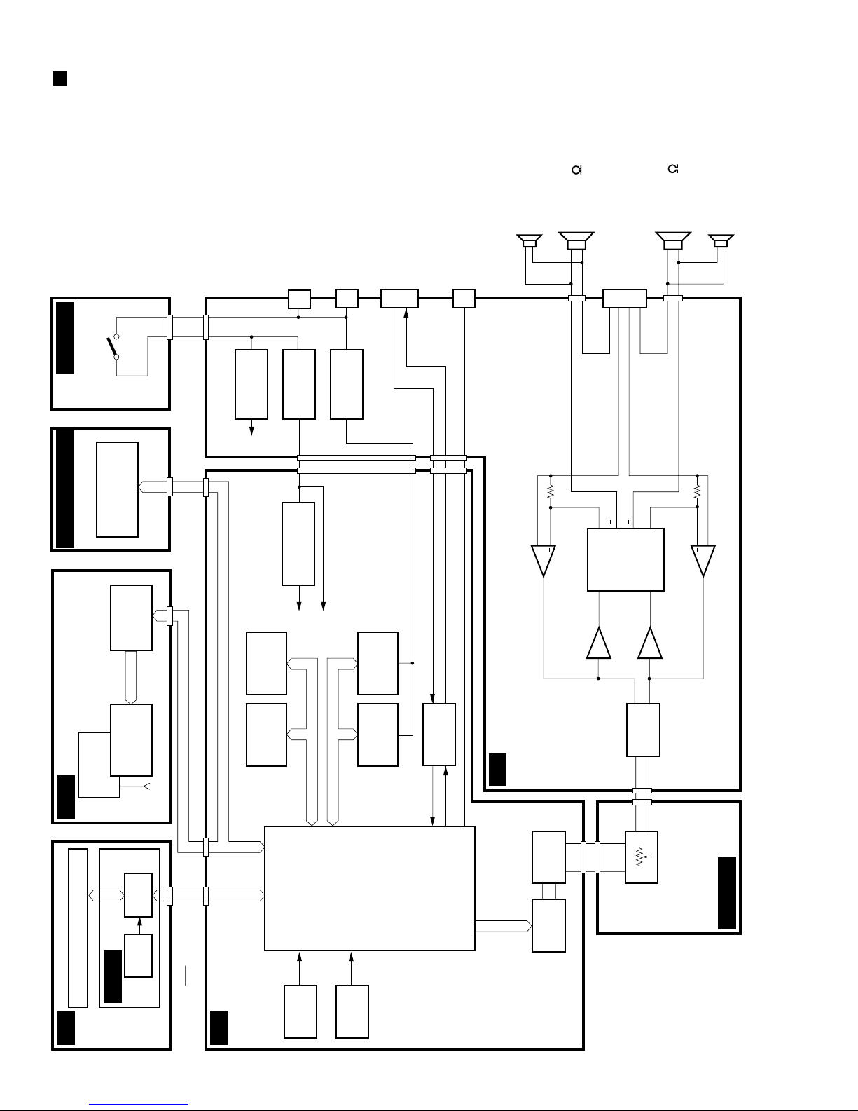
4. PN(VR), PN(PNL) Circuit Boards
4-1 Remove the lower case assembly. (See Procedure 1.)
4-2 Remove the AM circuit board. (See Procedure 2.)
4-3 PN(VR) Circuit Board:
Remove the three (3) screws marked [250D]. The PN(VR)
circuit board can then be removed. (Fig. 3)
4-4 PN(PNL) Circuit Board:
Remove the six (6) screws marked [250E]. The PN(PNL)
circuit board can then be removed. (Fig. 3)
5. PN(PNC), PN(PNR), LCD Circuit Boards
5-1 Remove the lower case assembly. (See Procedure 1.)
5-2 Remove the DM circuit board. (See Procedure 2.)
5-3 Remove the AM circuit board. (See Procedure 2.)
5-4 PN(PNC) Circuit Board:
Remove the three (3) screws marked [250F]. The PN(PNC)
circuit board can then be removed. (Fig. 3)
5-5 PN(PNR) Circuit Board:
Remove the eight (8) screws marked [250G]. The PN(PNR)
circuit board can then be removed. (Fig. 3)
5-6 LCD Circuit Board:
Remove the four (4) screws marked [250H]. The LCD unit
can then be removed. (Fig. 3)
Remove the eight (8) screws marked [L50]. The LCD circuit
board can then be removed. (Fig. 3)
* When re-install the LCD, place it so that the small protrusion
on the LCD faces the inside on the right. (Fig. 4)
6. Disassembling the keyboard assembly
6-1 Remove the keyboard assembly. (See Procedure 2.)
6-2 Remove the two (2) screws marked [30]. The MKS3 circuit
board can then be removed. (Fig. 2)
6-3 Remove the MK circuit board while pressing the fifteen
(15) hooks A inward, and then remove the rubber contact.
(Fig. 5)
6-4 Remove the twenty-one (21) screws marked [140], then
remove the black keys from the lower notes. Afterwards,
remove the white keys DFA and C' and then remove the
white keys CEGB from the higher notes. At this time, lift
the keys from the front and slide them towards you.The
keys can then be removed from the assembly. (Fig. 6)
Conductor side
• LCD unit
Rubber connector
Rubber connector
(Fig. 4)

(Fig. 8)
(Fig. 9)
(Fig. 7)
Rubber contact
Rubber contact
Hooks B
MK
PSR-280/PSR-282
11
7. Assembling the keyboard assembly
7-1 Install the white keys CEGB from the lower notes, and
then install the DFA keys and C' key. Afterwards install
the black keys from the higher notes, and tighten the
twenty-one (21) screws marked [140]. (Fig. 6)
7-2 Install the rubber contacts in the assembly while pressing
the keys as shown in Figure 9. Check that the rubber
contact has been firmly placed into position in the area
indicated by the arrow Figure 10.
* When fitting the rubber contacts, raise both ends of the
frame so that do not push the rubber contact up. Install the
MK circuit board in the assembly so that the hooks B hold
it as shown in Figure 11. (Fig. 7, 8, 9)
White Keys
Rubber contact
Hooks A
Black Keys
(Fig. 5)
MK Black Keys White Keys DFA
White Keys CEGB
White Key C'
[140]
[140]: Bind Head Tapping Screw-P 3.0 x 16 MFZN2Y (EP600310) or
[140]: Bind Head Tapping Screw-P 3.0 x 16 MFZN2BL (VB205200) or
[140]: Bind Head Tapping Screw-P 3.0 x 16 MFZN2B (VS756700)
(Fig. 6)

PIN
NO. I/O FUNCTIONNAME PIN
NO. I/O FUNCTIONNAME
1
2
3
4
5
6
7
8
9
10
11
12
13
14
15
16
17
18
19
20
21
22
23
24
25
26
27
28
29
30
31
32
33
34
35
36
37
38
39
40
41
42
43
44
45
46
47
48
49
50
51
52
53
54
55
56
57
58
59
60
61
62
63
64
65
66
67
68
69
70
71
72
73
74
75
76
77
78
79
80
81
82
83
84
ICN
RFCLKI
TM2
AVDD_PLL
AVSS_PLL
MODE0
VCC7
GND8
XIN
XOUT
MODE1
TEST0
TESTON
AN0-P40
AN1-P41
AN2-P42
AN3-P43
AVDD_AN
AVSS_AN
TXD0
TXD1
EXCLK
SMD11
SMD4
SMD3
SMD12
SMD10
SMD5
SMD2
SMD13
SMD9
SMD6
SMD1
SMD14
VCC35
GND36
SMD8
SMD7
SMD0
SMD15
SOE
SWE
SRAS
SCAS
REFRESH
CS0
SMA0
SMA16
VCC49
GND50
SMA1
SMA15
SMA2
SMA14
SMA3
SMA13
SMA4
SMA12
SMA5
GND60
VCC61
SMA11
SMA6
SMA10
SMA7
SMA9
SMA17
SMA8
SMA18
SMA19
SMA20
SMA21
SMA22
SMA23
CMA20
CMA19
VCC77
GND78
CMA18
CMA17
CMA5
CMA6
CMA4
CMA7
I
I
I
I
I
O
I
I
I
I
I
I
I
O
O
I
I/O
I/O
I/O
I/O
I/O
I/O
I/O
I/O
I/O
I/O
I/O
I/O
I/O
I/O
I/O
I/O
O
O
O
O
O
O
O
O
O
O
O
O
O
O
O
O
O
O
O
O
O
O
O
O
O
O
O
O
O
O
O
O
O
O
O
O
O
O
O
Initial clear
PLL Clock
PLL Control
Power supply
Ground
SWX dual mode
Power supply
Ground
crystal oscillator
crystal oscillator
SWX separate mode
TEST pin
TEST pin
A/D converter
A/D converter
A/D converter
A/D converter
Power supply
Ground
for MIDI or TO-HOST
for MIDI
Crystal oscillator
Wave memory data bus
Power supply
Ground
Wave memory data bus
read signal
write signal
RAS signal
CAS signal
REFRESH signal
CS signal
Memory address bus
Memory address bus
Power supply
Ground
Memory address bus
Memory address bus
Memory address bus
Memory address bus
Memory address bus
Memory address bus
Memory address bus
Memory address bus
Memory address bus
Ground
Power supply
Memory address bus
Memory address bus
Memory address bus
Memory address bus
Memory address bus
Memory address bus
Memory address bus
Memory address bus
Memory address bus
Memory address bus
Memory address bus
Memory address bus
Memory address bus
Program address bus
Program address bus
Power supply
Ground
Program address bus
Program address bus
Program address bus
Program address bus
Program address bus
Program address bus
85
86
87
88
89
90
91
92
93
94
95
96
97
98
99
100
101
102
103
104
105
106
107
108
109
110
111
112
113
114
115
116
117
118
119
120
121
122
123
124
125
126
127
128
129
130
131
132
133
134
135
136
137
138
139
140
141
142
143
144
145
146
147
148
149
150
151
152
153
154
155
156
157
158
159
160
161
162
163
164
165
166
167
168
CMA3
CMA8
CMA2
CRD
CMA1
CUB
VCC91
GHND92
CS1
CMA0
CLB
CMA12
CMA11
CMA10
CMA9
GND100
CWE
CMA16
CMA15
CMA14
CMA13
CMD8
CMD7
CMD9
CMD6
CMD10
CMD5
CMD11
CMD4
CMD12
CMD3
CMD13
CMD2
CMD14
VCC119
GND115
CMD1
CMD15
CMD0
CMA21
PDT15
PDT14
PDT13
PDT12
PDT11
PDT10
PDT9
PDT8
VCC133
GND134
PDT7
PDT6
PDT5
PDT4
PDT3
PDT2
PDT1
PDT0
VCA143
GND144
PAD2
PAD1
PAD0
VCC148
GND149
PCS
PWR
PRD
RXD0
RXD1
SCLKI
ADIN
ADLR
DO0
DO1
SYSCLK
VCC161
GND162
WCLK
QCLK
BCLK
SYI
IRQ0
NMI
O
O
O
O
O
O
O
O
O
O
O
O
O
O
O
O
O
O
I/O
I/O
I/O
I/O
I/O
I/O
I/O
I/O
I/O
I/O
I/O
I/O
I/O
I/O
I/O
I/O
O
I/O
I/O
I/O
I/O
I/O
I/O
I/O
I/O
I/O
I/O
I/O
I/O
I/O
I/O
I/O
I/O
I
I
I
I
I
I
I
I
I
I
O
O
O
O
O
O
O
I
I
I
Program address bus
Program address bus
Program address bus
read signal
Program address bus
high byte effective signal
Power supply
Ground
CS signal
Program address bus
low byte effective signal
Program address bus
Program address bus
Program address bus
Program address bus
Ground
write signal
Program address bus
Program address bus
Program address bus
Program address bus
Program memory Data bus
Power supply
Ground
Program memory Data bus
Program address bus
SWX access data bus
SWX access data bus
SWX access data bus
SWX access data bus
SWX access data bus
SWX access data bus
SWX access data bus
SWX access data bus
Power supply
Ground
SWX access data bus
SWX access data bus
SWX access data bus
SWX access data bus
SWX access data bus
SWX access data bus
SWX access data bus
SWX access data bus
Power supply
Ground
SWX access address bus
Power supply
Ground
Chip select
write enable
read enable
for Midi or TO-HOST
for Midi or Key scan
EXT Clock
A/D converter
A/D converter LR clock
DAC
DAC
1/2 clock
Power supply
Ground
for DAC LR clock
1/12 clock
IIS-DAC clock
Synch signal
Interrupt request
Interrupt request
HG73C205AFD (XU947C00) SWX00B (Tone Generator) DM: IC101
PSR-280/PSR-282
12
LSI PIN DESCRIPTION

PSR-280/PSR-282
13
PIN
NO. I/O FUNCTIONNAME PIN
NO. I/O FUNCTIONNAME
1
2
3
4
5
6
7
8
9
10
11
12
13
14
15
16
17
18
19
20
/RES
/INT
NUM
A7
A6
A5
A4
A3
A2
A1
A0
B0
B1
B2
B3
B4
B5
B6
B7
VSS
I
I
I
I/O
I/O
I/O
I/O
I/O
I/O
I/O
I/O
I/O
I/O
I/O
I/O
I/O
I/O
I/O
I/O
Reset
Interrupt request
Non-maskable interrupt
Port A
Port B
Ground
21
22
23
24
25
26
27
28
29
30
31
32
33
34
35
36
37
38
39
40
C7
C6
C5
C4
C3
C2
C1
C0
D0
D1
D2
D3/TX
D4/RX
D5//CK
D6//INT2
/STBY
TIMER
XTAL
EXTAL
VCC
I/O
I/O
I/O
I/O
I/O
I/O
I/O
I/O
I/O
I/O
I/O
O
I
O
I
I
I
O
I
Port C
Port D
(Serial data output)
(Serial data input)
(Clock for serial operation)
(Interrupt request 2)
(Standby mode signal)
Timer
Clock
Power supply
HD63B05V0F073P (XR951A00) CPU MKS3: IC1
PIN
NO. I/O FUNCTIONNAME PIN
NO. I/O FUNCTIONNAME
1
2
3
4
5
6
7
8
9
10
11
12
13
14
15
16
17
18
19
20
21
22
23
24
25
26
27
28
29
30
31
32
33
34
35
36
37
38
39
40
S22
S21
S20
S19
S18
S17
S16
S15
S14
S13
S12
S11
S10
S9
S8
S7
S6
S5
S4
S3
S2
S1
Vss
OSC1
OSC2
V1
V2
V3
V4
V5
CLK1
CLK2
Vdd
M
D
RS
R/W
E
DB0
DB1
O
O
O
O
O
O
O
O
O
O
O
O
O
O
O
O
O
O
O
O
O
O
I
O
O
O
O
O
I
I
I
I/O
I/O
Segment signal output for LCD
driving
Ground
Oscillator
Oscillator
Power supply
Data latch clock
Data shift clock
Power supply (+5 V)
Altamated signal for LCD driver outout
Display data interface
Read/write
Enable
Data interface
Data interface
41
42
43
44
45
46
47
48
49
50
51
52
53
54
55
56
57
58
59
60
61
62
63
64
65
66
67
68
69
70
71
72
73
74
75
76
77
78
79
80
DB2
DB3
DB4
DB5
DB6
DB7
C1
C2
C3
C4
C5
C6
C7
C8
C9
C10
C11
C12
C13
C14
C15
C16
S40
S39
S38
S37
S36
S35
S34
S33
S32
S31
S30
S29
S28
S27
S26
S25
S24
S23
I/O
I/O
I/O
I/O
I/O
I/O
O
O
O
O
O
O
O
O
O
O
O
O
O
O
O
O
O
O
O
O
O
O
O
O
O
O
O
O
O
O
O
O
O
O
Data interface
Common signal output for LCD
driving
Segment signal output for LCD
driving
KS0076BQ-00 (XV226A00) LCD DRIVER LCD: IC701

PSR-280/PSR-282
14
IC BLOCK DIAGRAM
µPC4570C (XC520A00)
Dual Operational Amplifier
DM: IC502
AM: IC810,820
µPD6379AGR (XR998A00)
D/A Converter
DM: IC501
1
2
3
4-V
8
7
6
5
Output A +V
Non-Inverting
Input A
-DC Voltage Supply
+DC Voltage
Supply
Output B
Inverting
Input B
Non-Inverting
Input B
Inverting
Input A
+-
+-
1
2
3
4LOUT
8
7
6
5
VDD
Ground
Lch analog
output
Power supply
Shift clock
Serial dat input
L/R clock
Voltage
reference
GND
REF
ROUT
CLK
SI
LRCK
Rch analog
output

2NA-V539790
Component side
Pattern side
to DM-CN701
2
LCD Circuit Board
CIRCUIT BOARDS
PSR-280/PSR-282
15
AM Circuit Board (XY426B0) ····················································································· 18
DM Circuit Board (XY036B0) ····················································································· 16
LCD Circuit Board (XY486B0) ··················································································· 15
MK-H Circuit Board (XR565B0) ················································································· 23
MK-L Circuit Board (XR564B0)·················································································· 22
MKS3 Circuit Board (XU878B0)················································································· 22
PN(PNC) Circuit Board (XY361A0)············································································ 18
PN(PNL) Circuit Board (XY361A0) ············································································ 20
PN(PNR) Circuit Board (XY361A0)············································································ 20
PN(PW) Circuit Board (XY361A0)·············································································· 18
PN(VR) Circuit Board (XY361A0) ·············································································· 18
Note: See parts list for details of circuit board component parts.

2NA-V533420
Component side
to HAMMER SENSOR-CN3
2
DM Circuit Board
from MKS-CN1
from PN(VR)-CN501from LCD-CN701from AM-CN601 from PN(PNR)-CN701 from AM-CN101
PSR-280/PSR-282
16

2NA-V533420
Pattern side
2
DM Circuit Board
IC101, IC501, IC301, 302 installation detailed drawing
IC101
character
direction
Pin 1 mark
IC501
character
Pin 1 mark
IC301,302
character
direction
Pin 1 mark
PSR-280/PSR-282
17

Component side
Component side
Component side
Component side
to Speaker-R
PN(PNC, PW, VR): 2NA-V534590
AM: 2NA-V534600 3
2
AM Circuit Board
PN(PNC) Circuit Board
PN(PW) Circuit Board
PN(VR) Circuit Board
to Speaker-L from LCD unit
from PN(PNL)-CN705
to DM-CN501
to DM-CN601 to DM-CN101
from Power supply
IN OUT
MIDI SUSTAIN DC IN to-12V
PHONES/
OUTPUT
VOICE
STANDBY/ON
STYLE SONG
MASTER
VOLUME
PSR-280/PSR-282
18

Pattern side
Pattern side
Pattern side
Pattern side
AM Circuit Board
PN(PNC, PW, VR): 2NA-V534590
AM: 2NA-V534600 3
2
PN(PNC) Circuit Board
PN(PW) Circuit Board
PN(VR) Circuit Board
PSR-280/PSR-282
19

PN(PNL, PNR): 2NA-V534590
Component side
Component side
to PN(PNC)-CN706
2
PN(PNL) Circuit Board
PN(PNR) Circuit Board
Overall
HARMONY
Yamaha Education Suite
Dict.
RLESSON L
TOUCH
to DM-CN702
TEMPO/TAP
FF
MAIN/AUTO FILL
REW
INTRO/ENDING
PAUSE
SYNC
START SYNC
STOP
A-B REPEAT
ACMP
ON/OFF
STYLE
SONG
START/STOP
START/STOP
321
654
987
+/YES 0 -/NO DJ Piano
RECORDSONG MEMORY
1AMEMORY12BANK 2345
METRONOME
Portable Grand & DJ
DEMO
Overall
REGISTRATION MEMORY
PSR-280/PSR-282
20
This manual suits for next models
1
Table of contents