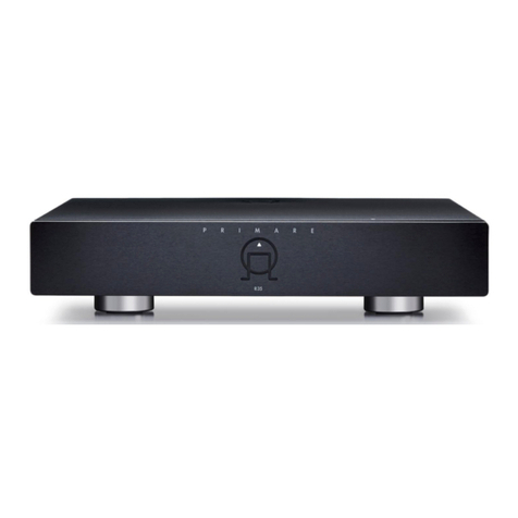
Primare A32 User manual

PRIMARE
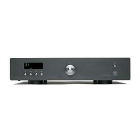
A32 Power Amplifier
Service Manual

1. Technical Description.
2. Error codes.
3. Bias Adjustment.
4. Schematics.
5. Technical Specifications.

A32 Functional Description
Features
The Primare A32 power amplifier is a fully balanced design, this means that the negative
speaker terminals are active, not ground as on an unbalanced design. When performing
measurements, test equipment (such as Audio Precision) that can handle balanced
amplifiers must be used.
The input impedance is 15K and the gain is 26dB. It is possible to obtain just above 250
undistorted watts at an 8R load (both channels driven). The frequency response are flat,
the A32 will drop down only -2dB at 100Khz.
Standby
The A32 is equipped with two standby modes, where standby mode 2 is the power save
mode. In power save mode only the standby circuit will be powered by the small standby
transformer placed on the digital PCB.
Digital control and monitoring
When power is first applied and the standby button on the front panel are pressed down
the A32 are going to initiate the startup sequence. Relay K1 will be turned on where after a
small delay will follow before relay K2 goes active to disable the inrush limiters. At the
same time bias are turned on by shutting down the voltage supplied to the optocouplers on
the amplifier channels. After a 20 second startup delay for the amplifier to settle down the
speaker relays are turned ON. During the startup sequence all safety parameters such as
DC-offset and fuses will be monitored, if an error is spotted the amplifier will refuse to start
and the standby LED will flash rapidly to indicate that an error has occurred. The error
code can be read out by pressing the error check switch (SW1). Description of the error
codes can be found on the next page.
If the standby switch is pressed when the amplifier is in operate mode it will go to standby
mode 1, which means that bias and speaker relay will be switched off. The standby LED is
going to half light intensity to indicate that the amplifier is in this standby mode.
If the standby button are pressed down for more than one second the amplifier are
shutting down into standby mode 2 which means that bias, speaker relay and the two
power relays K1, K2 are switched off. Only the standby circuit is still powered consuming
just a few watt of energy.
Temperature protection
When temperature has reached 70 centigrade at the temperature sensors the speaker
relay and bias are going to be switched off, when the temperature have decreased 10
centigrade the A32 are going to be restarted. In practice this will mean that the warmest
part of the heatsink will be around 75-80 centigrade when over- temperature protection
cuts in.

General Protection
During operation mode DC-offset, fuse, temperature and AC-loss are constantly
monitored, any abnormal function from these will immediately disengage the speaker relay
and the standby LED will start to flash rapidly indicating that an error has been spotted.
The error code can be checked by pressing the error check button (SW1), if more than one
error at the same time a repeated press of the button will display the next error.
DC-offset and over temperature will automatically resume to normal operation after a delay
if the error recovers. Fuse error will not (latch), here the amplifier must be turned off and
the fuses replaced before normal operation is possible.
Trigger.
If a 3.5mm teleplug are connected to the left trigger input (the right connector is the
output) the function of the standby button are being changed to only be able to turn the
amplifier into standby mode 2 directly. The standby button cannot turn the amplifier on
while the trigger is connected (trigger mode enable). The circuit will trigger at 2.5V and are
highly immune against disturbances. The trigger are only able to control the amplifier
between operate and standby mode 1.
RS232
The RS232 port can be used for firmware upgrading as well as controlling by Crestron
compatible RS232 codes.
Fuses
Due to the large capacitance of the electrolytics bank, turn off the mainspower and wait
minimum 15minutes before replacing a blown fuse. Make sure to replace a blown fuse with
exactly the same type and value.
Error codes
LEDNr
321Error
0 0 0 All OK
0 0 1 DC L+
0 1 0 DC L-
0 1 1 DC R+
1 0 0 DC R-
1 0 1 Fuse Rch
1 1 0 Fuse Lch
1 1 1 Overheated

Bias Adjustment
Critical for the adjustment are that the mainsvoltage is 230V or 120V exactly.
The temperature in the facility must be constant during the adjustment procedure.
Use the Bias test points and potentiometers (R1, R2) to adjust bias on each channel.
The lower potentiometer is accessible thru a hole in the bottom of the amplifier.
Bias test points
Compare the voltage
drop over all of the
emitter resistors.

These steps describe the Bias adjustment procedure, which is the same for both L& R
channels.
1. Switch the amplifier on or if it has been on burn-in (test), disconnect input signal and
loads. The A32 amplifier must be in operate mode, bias will be switched off in standby.
2. Let the amplifier run for 1h, without input signal.
3. Adjust the bias to 17mV measured on JP3, JP4 or JP2, JP1.
4. Check the maximum difference (voltage drop) over emitter resistors (R241, R243,
R245, R247, R239, R237, R235, R233, R240, R238, R236, R234, R242, R244, R246,
R248). The difference between them should not exceed 7mV. Higher difference might
be due to a faulty transistor or Emitter resistor, also check and that the screw are
tightened.
5. Wait 1h.
6. Measure the bias and if needed readjust to 17mV measured on JP3, JP4 or JP2, JP1.
7. Wait 1h.
8. Measure the bias and if needed readjust to 17mV measured on JP3, JP4 or JP2, JP1.
9. Wait 1h.
10.Measure the bias and if needed readjust to 17mV measured on JP3, JP4 or JP2, JP1.
Repeat step 5-9 until the bias are stabile.

12345678
A
B
C
D
8
7654321
D
C
B
A
Title
Number RevisionSize
A3
Date: 14-Nov-2005 Sheet of
File: C:\WORK\..\P2005-3D.SCH Drawn By:
C42200U/25V
S1
T500mA D12
BRIDGE1
1
2
3
4
5
6
7
8
9
10
J1
CON10
Bias L
SPK Relay L
XLR/RCA L
+15V L
Temp1 L
Temp2 L
GND L
Fuse L
DC-Check+ L
DC-Check- L
1
2
3
4
5
6
7
8
9
10
J2
CON10
Bias R
SPK Relay R
XLR/RCA R
+15V R
Temp1 R
Temp2 R
GND R
Fuse R
DC-Check+ R
DC-Check- R
R5
0R R6
0R R7
536R R8
560R
R9
2K2
R21
510R R24
10R
R26
4K7
R33
2R2 R34
2R2
SW BAL/UNBAL
Q1
BCV46
R10
2K2
R25
2K2
C1+ 1
V+ 2
C1- 3
C2+ 4
C2- 5
V- 6
T2OUT 7
R2IN 8
R1IN
13
R1OUT
12
R2OUT
9
VCC
16
GND
15
T1OUT
14
T2IN
10 T1IN
11
U2
MAX3232ECAE
1
2
3
4
P2
HEADER 4
1
2
3
F1
NMF40
1
2
3
F2
NMF40
C8
100N
C9
100N
C10
100N
C11
100N
C12
100N
+3.3V
RS232
NO1 1
N02
8
C1 2
C2
7
NC1 3
NC2
6
COIL 4
COIL
5
K1
RELAY DPDT3
7 8
6
3
2
5
4
1
D1
KB2855
R37
NTC 7R R38
NTC 7R
R39
NTC 7R
NO1 1
N02
8
C1 2
C2
7
NC1 3
NC2
6
COIL 4
COIL
5
K2
RELAY DPDT3
240V
120V
Q2 BCV46
R11
470R
Q4 BCV46
R12 470R
D2
BDY17D
D3
BDY17D
P2.0/ICB/DAC0/ADC03
1
P2.1/OCD/AD02
2
P0.0/CMP2/KBI0/AD01
3
P1.7/OCC/AD00
4
P1.6/OCB
5
P1.5/RST
6
VSS
7
P3.1/XTAL1
8
P1.0/TXD 18
P0.5/CMPREF/KBI5 22
VDD 21
P0.1/CIN2B/KBI1/AD10 26
P0.3/CIN1B/KBI3/AD12 24
P0.6/CMP1/KBI6 20
P0.2/CIN2A/KBI2/AD11 25
P1.1/RXD 17
P3.0/XTAL2/CLKOUT
9
P1.4/INT1
10
P1.3/INT0/SDA
11
P1.2/T0/SCL
12
P2.5/SPICLK 16
P0.4/CIN1A/KBI4/AD13 23
P2.2/MOSI
13
P2.3/MISO
14
P2.7/ICA 28
P0.7/T1/KBI7 19
P2.4/SS 15
P2.6/OCA 27
U3
P89LPC935
R13 10K
R14 10K
R15 10K
R16 10K
R27 10K
R28 10K
C13
100U/6.3V
C14
100U/6.3V
C15
100U/6.3V
C16
100U/6.3V
+3.3VD
X2
4MHZ
C17
10p
C18
22p
SER
14
SRCLK
11
SRCLR
10
RCLK
12
E
13
O0 15
O1 1
O2 2
O3 3
O4 4
O5 5
O6 6
O7 7
Q7 9
VCC
16
GND
8
U5
74LVC595
+3.3VD
R29
3K3
R30
3K3
R31
3K3
D9 LED
D10 LED
D11 LED
R40 412R
R41 110R
+3.3VD
C22
100N
D4
LL4148
D5
LL4148
R32
4K7
Q5
BC846
4
2
3
1SW1
SW-B3
R18
10K
+3.3VD
Check error
+3.3V
D6
LL4148
D7
LL4148
C23
100N
1
2
3
4
5
6
7
8
9
10
J3
CON10
1
2
3
4
5
6
7
8
9
10
J4
CON10
S2
NC
1
2
3
S3
SW-SPDT
+3.3V Standby mode
R19
4K7
+3.3V
+3.3VD
+3.3VD
R42
470K
C24
330N
D8
LL4148
+3.3VD
1
2
3
4
P5 HEADER 4
SW2
R20
1K
PIN4 ON P5
PIN3 ON P5
PIN2 ON P5 PIN1 ON P5
PCB 2
PCB3 PCB4
P6
PLUG
P7
PLUG
C1 47nF/275V X2
C2
47nF/275V X2
P1
PLUG
P3
PLUG
P4
PLUG
P8
PLUG
P9
PLUG
P10
PLUG
1
8
15
13
9
11
4
5
T1
TRANSF53X44
16
2
3
5
4SW3
SW120-240
240V
To mains Transformer
C19
100N C20
100N C25
10N
R43
10R
C26
100U/25V
J5
PHONEJACK STEREO SW
J6
PHONEJACK STEREO SW
C27
100N
R44
10R
C28
47u/16V
R1
2K2
R2
NC
R3
NC
Q6
BC846
Q7 BC846
R4
4K7
R22
4K7
+3.3VD
R23
10K
R45
10K
R46
10K Q3
BCV46
R47
10K
C29
100U/6.3V
C30
100U/6.3V
Vin
3
ADJ
1
Vout 2
U4
LD1085V33
C31
100n
C32
100n
C33
100U/6.3V
+3.3VD
+3.3VD
D13
LL4148
D14
LL4148
D15
LL4148
D16
LL4148
D17
LL4148
D18
LL4148
D19
LL4148
D20
LL4148
D21
LL4148 D22
LL4148
D23
LL4148
D24
LL4148


1 2 3 4 5 6 78
A
B
C
D
8
7654321
D
C
B
A
Title
Number RevisionSize
A2
Date: 7-Dec-2005 Sheet of
File: C:\WORK\..\P2005-8C.SCH Drawn By:
Q1
2SC2240
Q9
2SA970
Q13
BD677A
Q15
2SC5171
Q66
2SA1930
R1
1K
Q69
2SA1943
Q77
2SC5200
R3
33K
R7
10K
R11
110R
R13
470R
D1
1N4148
D2
1N4148
C1
0.1U
R31
5K6
R32
5K6
R35
5K6
R40
3K3
Q10
2SA970
R42
15K
R43
12K
C14
22PF
Q22SC2240
Q3
2SC2240
Q4
2SC2240
R46
133R
R48
1K5
R14
470R
R207
1K
R209
22K
C84
39P
D3
1N4148
D4
1N4148
C2
0.1U
R15
470R
R213
220R R217
100R
R16
470R
R221
4K7
R222
4K7
R223
4K7
R229
470K
A
1
K
2
C4
E3
Q85
OPTOISO1
1
2
3
Q87
BS107
R214
330R
R231
680R
R224
2K2
R49
1K1
Q17
2SC5171
R17
56R
R18
56R
C4
0.1U
C86
220U/16V
R19
220R
R20
220R
R233
0.22R
R234
0.22R
R249
22R
R250
22R
R251
22R
R252
22R Q70
2SA1943
Q78
2SC5200
R235
0.22R
R236
0.22R
R253
22R
R254
22R
R255
22R
R25622R
S1
6.3A
S2
6.3A
C88
100N
C89
100N
R210
22K
R283
1K
C5
0.1U C90
1U
R296
1M
+15V
-15V
C6
0.1U
C94
0.1U
C96
100U/63V
C97
100U/63V
R298
4R7
C7
0.1U
R21
470R BIAS
Q89A
2SK389 Q89B
2SK389
+50V
-50V
U1
TL071
R284
1K1 C110
NC
1
2
JP3
C98
100U/63V
C99
100U/63V
Q71
2SA1943
Q79
2SC5200
R237
0.22R
R238
0.22R
R257
22R
R258
22R
R259
22R
R260
22R
Q72
2SA1943
Q80
2SC5200
R239
0.22R
R240
0.22R
R261
22R
R262
22R
R263
22R
R26422R
R285
1K
R300
15K
R218
100R
R286
1K
R219
100R
R287
1K
R301
22K
R302
22K
C112
330P
C113
330P C114
330P
3
21
84
U9A
OPA2134
5
67
U9B OPA2134
3
21
84
U10A
OPA2134
5
67
U10B
OPA2134
S4A
SW SPDT
S4B
SW SPDT
4 5
S4C
R288
1K
R289
1K
R290
1K
R291
1K
R303
47K
R304
47K
R265
22R
R266
22R
Q5
2SC2240
Q11
2SA970
Q14
BD677A
Q18
2SC5171
Q67
2SA1930
1
W
2
R2
1K
Q73
2SA1943
Q81
2SC5200
R4
33K
R8
10K
R12
110R
R22
470R
D17
1N4148
D18
1N4148
C8
0.1U
R37
5K6
R38
5K6
R39
5K6
R41
3K3
Q12
2SA970
R44
15K
R45
12K
C15 22P
Q62SC2240
Q7
2SC2240
Q8
2SC2240
R47
133R
R50
1K5
R23
470R
R208
1K
R211
22K
C85
39P
D19
1N4148
D20
1N4148
C9
0.1U
R24
470R
R215
220R R220
100R
R25
470R
R225
4K7
R226
4K7
R227
4K7
R230
470K
A
1
K
2
C4
E3
Q86
OPTOISO1
1
2
3
Q88
BS107
R216
330R
R232
680R
R228
2K2
R51
1K1
Q64
2SC5171
R26
56R
R27
56R
C10
0.1U
C87
220U/16V
R28
220R
R29
220R
R241
0.22R
R242
0.22R
R267
22R
R268
22R
R269
22R
R270
22R Q74
2SA1943
Q82
2SC5200
R243
0.22R
R244
0.22R
R271
22R
R272
22R
R273
22R
R27422R
C91
100N
C92
100N
R212
22K
R292
1K
C11
0.1U C93
1U
R297
1M
+15V
-15V
C12
0.1U
C95
0.1U
C100
100U/63V
C101
100U/63V
R299
4R7
C13
0.1U
R30
470R BIAS
Q90A
2SK389 Q90B
2SK389
+50V
-50V
3
2
6
74
U8
TL071
R293
1K1 C111
NC
C102
100U/63V
C103
100U/63V
Q75
2SA1943
Q83
2SC5200
R245
0.22R
R246
0.22R
R275
22R
R276
22R
R277
22R
R278
22R
Q76
2SA1943
Q84
2SC5200
R247
0.22R
R248
0.22R
R279
22R
R280
22R
R281
22R
R28222R
C3
2200U/50V
C17
2200U/50V
C182200U/50V C192200U/50V
C119 100NC120 100N
R306
10R
R307
10R
C127
220U/35V
C128
220U/35V
+15V
-15V
Vin
1
GND
2
OUT 3
U11
7815
Vin
2
GND 1
OUT 3
U12
7915
Q65 2SC4793
Q68
2SA1837
R52
2K2
R206
2K2
C129
470U/35V
C130
470U/35V
D23
24V
D24
24V
C131
10U/50V
C132
10U/50V
+50V-POWER
-50V-POWER
+50V-POWER
-50V-POWER
+50V-POWER +50V
-50V-50V-POWER
C121
100N
+15V
+15V
-15V
-15V
-15V
+15V
C122
100N
C123
100N C124
100N
C125
100N
C126
100N
C133
220U/50V
C134
220U/50V
1
2
JP4
C106
100U/63V
C107
100U/63V
C108
100U/63V
C109
100U/63V
1
2
3
4
5
6
7
8
9
10
J6
CON10
BIAS
SPK-RELAY
FUSE-ERROR
R5
20K
R6
20K
FUSE-ERROR
DC-CHECK +
DC-CHECK -
DC-CHECK -
DC-CHECK +
Q91
BC846
D21
1N4007
R309
560R/3W
12
3
4 5
S8
RELAY-SPDT
R310
100K
R294
4K7
SPK-RELAYQ92
BC846
D22
1N4148
R311
100K
R295
4K7
XLR/RCA
+15V R312
100R
XLR/RCA
R9
10K
R10
10K
C16
NC
C83
NC
+15V
C20
2200U/50V
C21
2200U/50V
C22
2200U/50V
C232200U/50V
C242200U/50V
C252200U/50V
C26
1U/250V
C27
1U/250V
C28 100NC29 100N
C30
100n
C31
100n
C32
100n
C33
100n
RV1
KTY81
OUT(+)
OUT(-)
C34
100N
C35
100N
C36
10N R33
10R
R34
0R
R36
0R
R53
100R
R54
100R
R55
100R
GND
XLR+
XLR-
RCA IN
RCA-GND
C37
100U/50V
R56
1K
R57
1K
R58
1K R59
1K
1
2
JP1
1
2
JP2
R60
10R
R61
10R
R62
10R
R63
10R


1 2 34
A
B
C
D
4
321
D
C
B
ATitle
Number RevisionSize
A4
Date: 7-Dec-2005 Sheet of
File: C:\WORK\..\P2005-4B.SCH Drawn By:
D1
BRIDGE1
C1
15000/63V
C2
15000/63V
C3
15000/63V
C4
15000/63V
C5
15000/63V
C6
15000/63V
D2
BRIDGE1
D3
BRIDGE1
C7
15000/63V
C8
15000/63V
C9
15000/63V
C10
15000/63V
C11
15000/63V
C12
15000/63V
D4
BRIDGE1
P1
PLUG
P2
PLUG
P3
PLUG
P4
PLUG
P5
PLUG
P6
PLUG
P7
PLUG
P8
PLUG
P9
PLUG
P10
PLUG
P11
PLUG
P12
PLUG
P13
PLUG
P14
PLUG
R1
MRS25
R2
MRS25
R3
22k
R4
22k


Performance Data
2000VA Torodial Transformer.
A total of 180 000 uF electrolytes in the powersupply.
Dual set of Speakerterminals for each channel.
Balanced (RCA) and Unbalanced (XLR) inputs.
Input impedance 15K, RCA and XLR
Output Power (both channel driven): 2x250W 8Ohms load 20Hz-20Khz
2x400W 4Ohms load 20Hz-20Khz
THD+N below 0.05% in both cases.
Frequency response: 20Hz-100Khz –0.5dB
Noise, below –100dBV
THD+N: 1K 250W 8R load below 0.01%.
Gain: 26dB unbalanced, 20dB balanced.
Trigger input range: 4-15V.
Other manuals for A32
2
Table of contents
Other Primare Amplifier manuals
Primare
Primare A33.2 User manual
Primare
Primare SP33 User manual
Primare
Primare A34.2 User manual
Primare
Primare I30 User manual
Primare
Primare SPA21 User manual
Primare
Primare A60 User manual
Primare
Primare A30.1 MK2 User manual
Primare
Primare A31.2 User manual
Primare
Primare I15 User manual
Primare
Primare R32 User manual
Primare
Primare R20 MM-MC User manual
Primare
Primare A30.5 User manual
Primare
Primare A30.7 User manual
Primare
Primare DAC30 User manual
Primare
Primare A35.2 User manual
Primare
Primare A35.8 User manual
Primare
Primare PRE35 User manual
Primare
Primare PRE32 User manual
Primare
Primare R15 User manual
Primare
Primare I20 User manual
