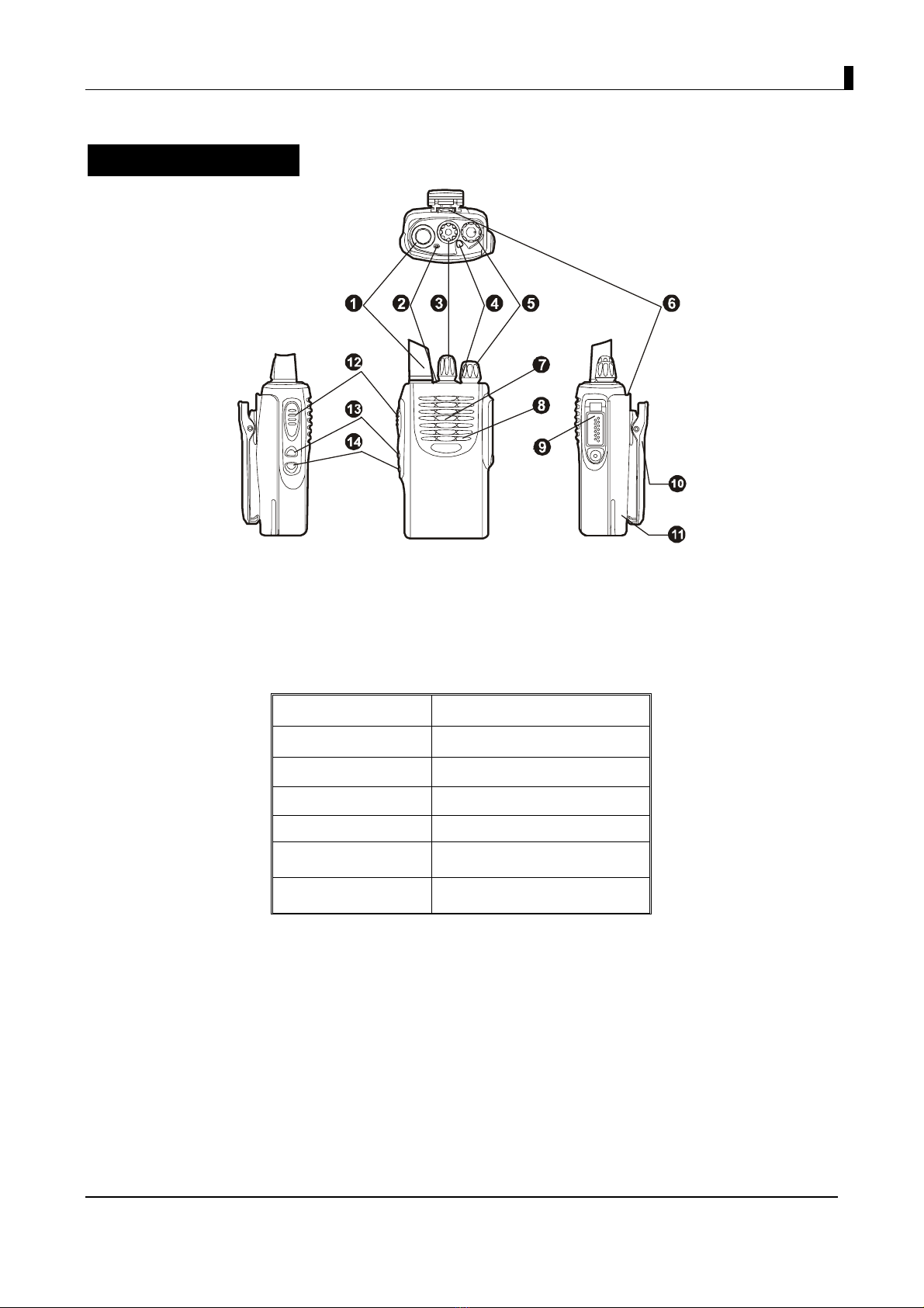
RP3000 Circuit Description
- 9 -
1) PLL
IC400 is a divider. Step frequency of PLL circuit is 2.5 KHz or 6.25 KHz. A 16.8MHz reference
oscillator signal is divided at IC400 by a fixed counter to generate a 2.5 KHz or 6.25 KHz reference
frequency. Output signal from VCO is buffer amplified by Q416 and divided at IC400 by a frequency
divider. Divided signal is compared in the phase comparator with 2.5 KHz or 6.25KHz reference
signal of IC400. Output signal from phase comparator is filtered through a low pass filter and
passed to the VCO to control oscillator frequency.
2) VCO
The operating frequency is generated by Q352 in transmit mode and by Q350 in receive mode.
Operating frequency generates a control voltage by phase comparator to control varactor diodes so
that the oscillator frequency is consistent with the MCU preset frequency (D350, D352, D354 and
D355 in transmit mode and D351, D353, D356 and D357 in receive mode). T/R pin is set high level
in receive mode and low in transmit mode. The output from Q352 and Q350 is amplified by Q354
and sent to buffer amplifier.
3) Unlock Detector
An unlock condition appears if low level appears at LOCK pin of IC400. Transmission is forbidden if
this condition is detected by microprocessor.
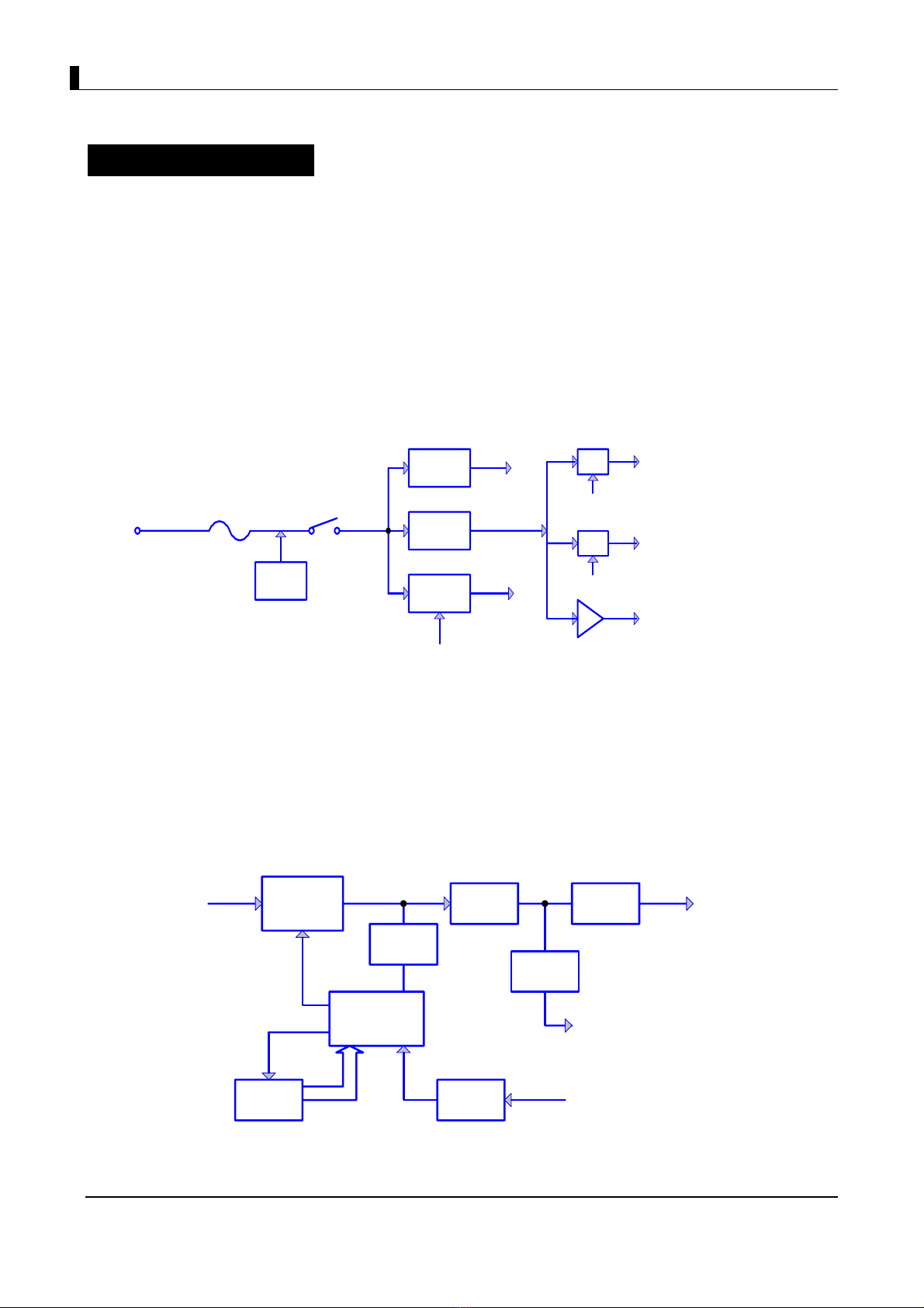
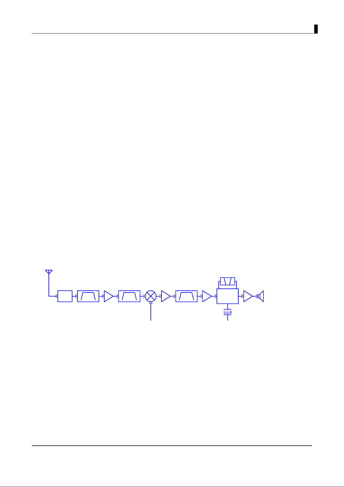
3. Receiver
The receiver utilizes double conversion superheterodyne.
C
ANT
ANT
SW
BPF Q201
RF AMP
BPF
MCF
XF201
IF AMP
Q222
MIXER
IC218
CF201,202
IF,MIX,DET
IC204
AF AMP
IC720 SP
1st Local OSC
(PLL)
2nd Local OSC
IF AMP
Q216
Fig.3 Receiver Section Configuration
1) Front-end Amplifier
The signal from antenna is amplified at RF amplifier (Q201) after passing through a
transmit/receive switch circuit and a band pass filter. The amplified signal is filtered
through a band pass filter to remove unwanted signals before it passes the first mixer.
2) First Mixer
The signal from RF amplifier is mixed with the first local oscillator signal from PLL frequency
synthesizer circuit at the first mixer (IC218) to create a 44.85MHz first IF signal. The first IF signal is
then fed through a crystal filter (XF201) to further remove spurious signals from adjacent channel.