Teac AG-D7900 User manual

AAGG--DD77990000
SERVICE MANUAL
AV Digital Home Theater Receiver
Effective : February, 2002 S-0000A
NOTES
●PC boards shown are viewed from parts side.
●The parts with no reference number or no parts number in the
exploded views are not supplied.
●As regards the resistors and capacitors, refer to the circuit diagrams
contained in this manual.
●£Parts marked with this sign are safety critical components. They
must be replaced with identical components - refer to the appropriate
parts list and ensure exact replacement.

2
CONTENTS
SPECIFICATIONS.................................................................................................................................3
SAFETY INSTRUCTIONS ...................................................................................................................4
MEASUREMENTS AND ADJUSTMENTS ........................................................................................5
FIP DISPLAY ........................................................................................................................................8
DISPLAY PIN CONNECTION ..............................................................................................................9
IC BLOCK DIAGRAMS AND PIN FUNCTIONS ................................................................................10
EXPLODED VIEWS AND PARTS LIST .............................................................................................22
PC BOARDS AND PARTS LIST ........................................................................................................24
INCLUDED ACCESSORIES ...............................................................................................................30

3
Amplifier Section
Surround Output Power (0.9 % THD, 1 kHz, 8 ohms):
60 + 60 watts (Front)
60 watts (Center)
60 + 60 watts (Rear)
Delay Time:
DOLBY DIGITAL: REAR 0 – 15 ms
CENTER 0 – 5 ms
DOLBY PRO LOGIC: REAR 15 – 30 ms
Audio Input Sensitivity/Impedance:
*LINE: 220 mV/47 k ohms
Output Level/Impedance:
CD-R/TAPE REC: 200 mV/2.2 k ohms
Frequency Response:
*LINE: 20 Hz – 65 kHz, +1/ –3 dB
Signal-to-Noise Ratio:
*LINE: 95dB (IHF-A)
Tone Control:
BASS: ± 10 dB at 100 Hz
TREBLE: ± 10 dB at 10 kHz
Digital Audio Section
Sampling Frequency: 32 kHz, 44.1 kHz, 48 kHz, 96 kHz
DIGITAL Input Level/Impedance:
DIGITAL 1, 2 (OPTICAL): –15 dBm — –21 dBm
DIGITAL 3 (COAXIAL): 0.5 Vp-p / 75 ohms
FM Tuner Section
(Without notes 100.1 MHz, 65 dBf)
Tuning Range:
87.5 MHz – 108.0 MHz (100 kHz steps)
Usable Sensitivity (IHF):
Mono: 11.2 dBf
50 dB Quieting Sensitivity:
Mono: 15.3 dBf
Stereo: 38.5 dBf
Capture Ratio: 2.0 dB
Image Rejection Ratio: 45 dB
AM Suppression Ratio: 55 dB
Total Harmonic Distortion (1 kHz):
Mono: 0.4%
Stereo: 0.5%
Frequency Response: 30 Hz – 15 kHz, +1/ –1.5 dB
Stereo Separation (1 kHz): 40 dB
Signal-to-Noise Ratio:
Mono: 75 dB
Stereo: 70 dB
AM Tuner Section
Tuning Range:
530 kHz – 1,720 kHz (10 kHz steps)
Usable Sensitivity: 55 dB/m
Total Harmonic Distortion: 0.8% at 85 dB/m
Signal-to-Noise Ratio: 45 dB at 85 dB/m
Video Section
Input Sensitivity/Impedance: 1.0 Vp-p/75 ohms
Output Level/Impedance: 1.0 Vp-p/75 ohms
General
Power Requirements:
120 V AC, 60 Hz (U.S.A./ Canada model)
120/230 V AC, 50-60Hz (General Export model)
Power Consumption:
2.5 A
AC Outlets:
Switched x 2, Total 100 W max. (1 A max.)
Dimensions (W x H x D)
435 x 165 x 350 mm (17-1/8" x 6-1/2" x 13-3/4")
Weight (net):
8.2kg (18-1/16lbs) (U.S.A./ Canada model)
8.4kg (18-1/2lbs) (General Export model)
Standard Accessories:
AM Loop Antenna x 1
FM T-type Antenna x 1
Remote Control Unit (UR-417) x 1
*LINE means CD, CD-R/TAPE, VCR/VIDEO 1, DBS/VIDEO 2,
DVD/VIDEO 3 and AUX/VIDEO 4.
<Improvements may result in specifications and features
changing without notice.
<Illustrations may differ slightly from production models.
SPECIFICATIONS

4
SAFETY INSTRUCTIONS
PRECAUTIONS DURING SERVICING
1. Parts identifide by the ( )symbol parts are critical
for safety. Replace only with parts number specified.
2. In addition to safety, other parts and assemblies are
specified for conformance with such regulations as
those applying to spurious radiation.
These must also be replaced only with specifide
replacements.
Examples :RF converters, tuner units, antenna
selectswitches, RF cables, noise blocking capacitors,
noise blocking filters, etc.
3.
Use specified internal wiring. Note especially :
1) Wires covered with PVC tubing
2) Double insulated wires
3) High voltage leads
4. Use specified insulating materials for hazardous live
parts. Note especially:
1) Insulation Tape
2) PVC tubing
3) Spacers(insulating barriers)
4) Insulation sheets for transistors
5) Plastic screws for fixing micro switches
5. When replacing AC primary side components
(transformers, power cords, noise blocking
capacitors, etc.), wrap ends of wires securely about
the terminals before soldering.
6. Make sure that wires to do not contact heat
producing parts (heat sinks, oxide metal film
resistors, fusible resistors, etc.).
7. Check that replaced wires do not contact sharp
edged or pointed parts.
8. Also check areas surrounding repaired locations.
9. Make sure that foreign objects (screws, solder
droplets, etc.) do not remain inside the set.
MAKE YOUR CONTRIBUTION TO PROTECT
THE ENVIRONMENT
Used batteries with the ISO symbol for recycling
as well as small accumulators (rechargeable
batteries), mini-batteries (cells) and starter
batteries should not be thrown into the garbage
can.
Please leave them at an appropriate depot. All other house-
hold batteries can be thrown out with the household waste.
SAFETY CHECK AFTER SERVICING
After servicing, make measurements of leakage-current
or resistance in order to determine that exposed parts
are acceptably insulated from the supply circuit.
The leakage-current measurement should be done
between accessible metal parts (such as chassis,
ground terminal, microphone jacks, signal input/output
connectors, etc.) and the earth ground through a
resister of 1500 ohms paralleled with a 0.15
capacitor, under the unit's normal working conditions.
The leakage-current should be less than 0.5mA rms AC.
The resistance measurement should be done between
accessible exposed metal parts and power cord plug
prongs with the power switch (if included) "ON". The
resistance should be more than 2.2M Ohms.
PRECAUTIONS IN REPAIRING
When repairing or adjusting the unit, please note the
following points.
1. Do not put excessive pressure on the mechanical
part (operation part), including the pick-up block, as
extremely high mechanical precision is required in
these parts.
2. When the base is removed for repair adjustment,
make sure that there are no metal obiects in the
narrow gap between the P. C. board or the mecha
parts and the base
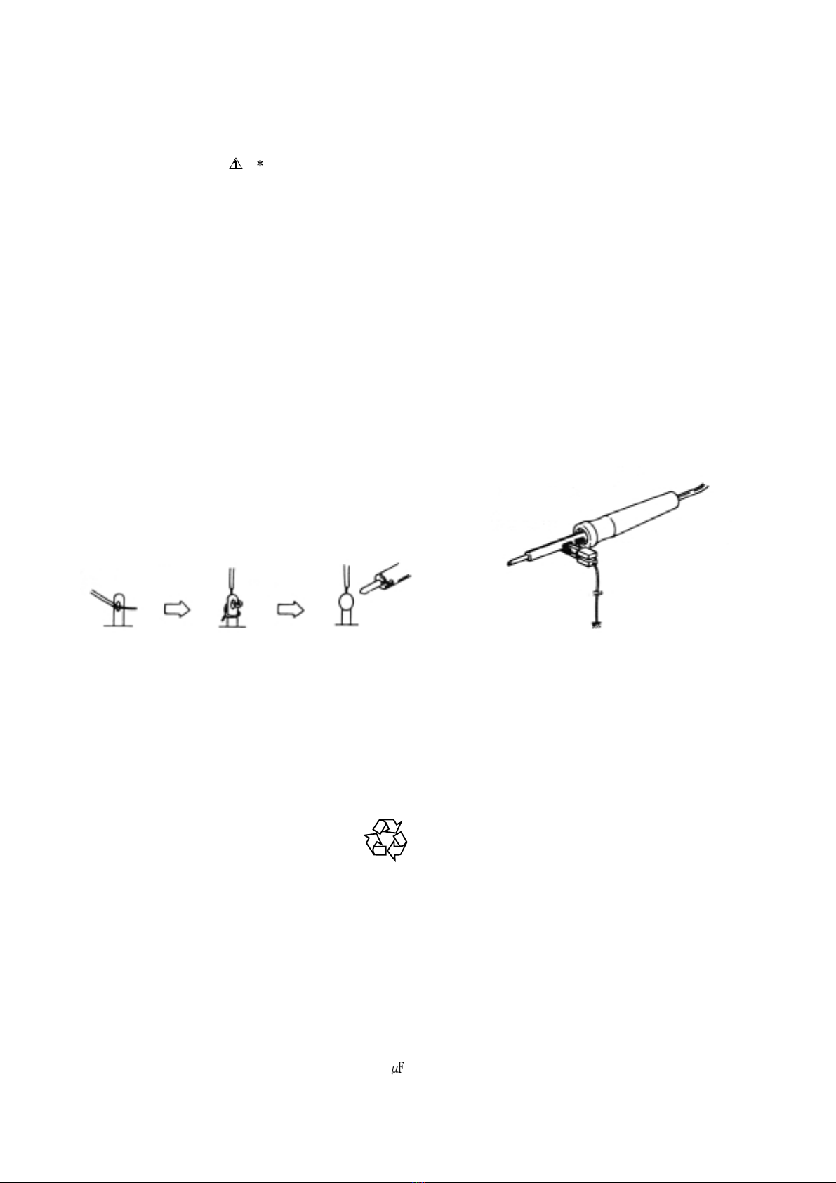
3. The Micro-Computer and the CD signal processing
ICs can be damaged by static electricity or leakage
from a soldering iron during repairing. While
soldering, please take the precautions against
leakage as in the illustration.
4. Do not loosen any screws in the pick-up block.
When handing the pick-up block, please refer to the
points to NOTE when replacing the pick-up block.
5. Keep safety for hazardous invisible Laser Radiation,
DO NOT watch the Laser Beam (Objective lens)
directly.
6. Models for some countries, laser warning labels are
affixed on the unit and inside of the unit, as shown
below. Read it carefully for your safety, when
repairing or adjusting the unit.
GND

ALIGNMENT INSTRUCTIONS
EQUIPMENT NEEDED:
AM Signal Generator
FM Signal Generator
Oscilloscope
VTVM(AC, DC)
Test loop antenna (AM Adjustment)
Dummy antenna (FM Adjustment)
Distortion analyser
IMPORTANT
1. Check power-source voltage.
2. Set the function switch to band aligned.
3. Keep the signal input as low as possible to adjust accurately.
4. Modulation and modulation frequency.
Item Modulation Modulation frequency
Band
AM 30% 400Hz
FM 400Hz
ADJUSTMENT POINT
MEASUREMENTS AND ADJUSTMENTS
100% (40 kHz Dev.) [E/UK]
100% (75 kHz Dev.) [US]
AM LOOP ANT
ANT TERMINAL
CT10 PACK1
IC11
J208
VR11 VR13
IC12
T102
FM ANT
VR12
J207
J205
L104 L105
T101
<PACK DETAIL>
(FOR UL ersion)
L3
L7
L4
L5
L6
L3
L7
T1
L6
L4L5
L3
L6
L4
FM OSC COIL
T1 FM IFT
FM OFFSET ADJ TP
CT10 AM ANT TRIMMER (1503kHz/1510kHz)
L104 AM ANT COIL
L105 AM OSC COIL
T101 FM IFT COIL
T102 AM IFT COIL (612kHz/610kHz)
VR13 FM SD ADJUSTMENT
VR12 AM SD ADJUSTMENT
VR11 FM SEPARATION ADJ
J208 FM/AM VT
J205
J207
FM ANT COIL
FM RF COIL
(FOR EUR ersion)
L1
L2
L6
L3
L4
L5
L1L2
L5
L7
IFT
FM OSC COIL
L7
FM ANT COIL
FM RF COIL
5

1.TUNING FREQUENCY RANGE ADJUSTMENTS
(FM) DC VOLTMETER ................ CONNECT TO TEST POINT J208 and GND
NO. Band Frequency Adjust for Adjustment
1 FM 87.50MHz 1.6V L7
2 AM 530 kHz 1V L105
[US/C] [530 kHz] [1V] [L105]
2.AM TRACKING ADJUSTMENT
Signal Generator........................ Connects to the AM ANT. Coil through the loop antenna.
Adjust for the indication of VTVM of the wave form of scope to be maximum.
BAND Step Frequency Adjust for Adjustment
1 610 kHz Maximum sensitivity T102, L104
[US/C] [610 kHz] Maximum sensitivity T102, L104
2 1510 kHz Maximum sensitivity CT10
[US/C] [1510 kHz] Maximum sensitivity CT10
3 Repeat steps 1 and 2 several times.
AM
J208
3.FM-RF ADJUSTMENT
Signal Generator........................ Connect to FM ANT JACK (FM IN) through the dummy.
NO. Frequency Adjust for Adjustment
1 90.10MHz Maximum Sensitivity L3, L5, L6
2 Repeat step 1 several times.
6

4.FM MONO DISTORTION ADJUSTMENT
DC VOLT METER........................Connect to J205 (-), J207 (+) through the chock coil (100uH).
Signal Generator........................Connect to FM ANT Jack (FM IN) through the dummy.
Distortion Meter.........................Connect to the output.
NO. Frequency Adjust for Adjustment
1 100.10MHz
2 100.10MHz
3 Repeat steps 1 and 2 several times.
5.FM/AM AUTO STOP LEVEL ADJUSTMENT
FM Signal Generator..................Connect to FM ANT Jack (FM IN) through the dummy.
AM Signal Generator.................Connect to AM ANT. Coil through the Loop antenna.
J205
J207
DC Voltmeter 0V
Minimum T.H.D
7
DC Voltmeter 0V T101
T101
BAND Step Signal Generator Adjust for Adjustment
1 990KHz 82dB Display ON VR12
[US/C] [990KHz]
2 990KHz 81dB Display OFF VR12
[US/C] [990KHz]
1 100.1MHz 32dB Display ON VR13
2 100.1MHz 31dB Display OFF VR13
TUNED
TUNED
TUNED
TUNED
AM
FM

8
10G 9G 8G 7G 6G 5G 4G 3G 2G 1G
P1 SOURCE d2 d2 d2 d2 d2 d2 d2 d2 kHz
P2 AUX d1 d1 d1 d1 d1 d1 d1 d1 1d
P3 LD e e e e e e e e 1e
P4 DVD r r r r r r r r 1c
P5 VCR 1 p p p p p p p p 1g
P6 REC n n n n n n n n 1f
P7 c c c c c c c c 1b
P8 SP. f f f f f f f f 1a
P9 A g g g g g g g g M
P10 B m m m m m m m m 2d
P11 CHURCH h h h h h h h h 2e
P12 DISCO j j j j j j j j 2c
P13 STADIUM k k k k k k k k 2g
P14 HALL b b b b b b b b 2f
P15 THEATER a2 a2 a2 a2
a2
a2 a2 a2 2b
P16 PCM a1 a1 a1 a1 a1 a1 a1 a1 2a
P17 AC-3 S1 S1 S1 S1 S1 S1 S1 S1
DELAY.T
P18 STEREO S2 S2 S2 S2 S2 S2 S2 S2
PRESET CH.
P19 3 S3 S3 S3 S3 S3 S3 S3 S3 MEMO
P20 S4 S4 S4 S4 S4 S4 S4 S4 TAPE
P21 DIGITAL RDS Dp TA MHz
P22
PRO LOGIC
DTS TUNED STEREO PTY RT TP mS
ANODE CONNECTION
FIP DISPLAY

9
Pin No.
46 47
F1 F1
Pin No.
31 32 33 34 35 36 37 38 39 40 41 42 43 44 45
NX NX NX NX 1G 2G 3G 4G 5G 6G 7G 8G 9G 10G NP
Pin No.
16 17 18 19 20 21 22 23 24 25 26 27 28 29 30
P14 P13 P12 P11 P10 P9 P8 P7 P6 P5 P4 P3 P2 P1 NX
Pin No.
1 2 3 4 5 6 7 8 9 10 11 12 13 14 15
F2 F2 NP NX NX NX NX P22 P21 P20 P19 P18 P17 P16 P15
Connection
Connection
Connection
Connection
PIN CONNECTION
47 1

PIN No. SYMBOL I/O DESCRIPTION
1,25 VDD - Power Supply Port(+5V)
2,3 Function SW1,SW2 I Function Encoder Control Port
4 Speaker ON/OFF O Front Speaker Relay Drive Port(“H”)
5 NC - Not Use(No connection)
6 DSP Reset O Reset (Initial Clear) Port for YSS912
7 Surr. CLK O Surr. CLK Output Port
8 DATA OUT O Data Output Port for YSS912
9 Surr. DATA O Surr. DATA Output Port
10 CS O Chip Selector Port for YSS912
11 CS O Chip Selector Port for AK4112
12 CSBN O Sub DSP Chip Selector for YSS912
13,14 RDS CLK/DATA I RDS IC(SA6579TV1) CLK/DATA Port
15 Stereo IN I Stereo Display Control Port("L")
16 Tuned IN I Tuned Display Control Port("L")
17 ~ 21 KEY Matrix I Resistor Divide Key Control Input (17,18 Pin: NOT USE)
22,30 Vss - Device GND Port
23 Vass - Device Analog GND Port
24 Varef - A/D Converter Reference Voltage
26 BACKUP I Back Up Mode Control Input
27 TEST - NC(GND)
28,29 VOLUME UP/DOWN I Master Volume Up/Down Control Port
31 X IN I 8MHz Crystal Connection Port
32 X OUT O
33 RESET (L) I Reset Input
34 REMOTE IN I Remote Control Sensor Data Input
35 BUS IN(NC) I System Remote Control Input(No Connection))
36 HEADPHONE IN O Headphone JACK INPUT(“H”) - Connet to GND
37 E.VOL.DATA O
38 E.VOL.CLK I Electronic Vol. IC(M62446FP) DATA/CLK/STB Port
39 E.VOL.CE O
40 PLL.DATA IN I PLL IC (LC72131) DATA Input Port
41 PLL.CE O PLL IC (LC72131) Chip Enable Control Port
42 DATA 3 O Function IC Data Input Port
43 CLK 3 O Func./PLL IC CLK Control Port
44 FUNC. STB O Function Strobe Control Output
45 FUNC. MUTE O Function Mute Control Output(“H”)
46 SURR. MUTE O Surrounc Mute Control Output(“H”)
47 Power ON/OFF O Power ON/OFF Control Port("H")
48 SURR. H O Surr. ON/OFF Contol Port("H")
49 PROTECT IN I Protect Input Port("L")
50 FIP Vkk - FIP (FLT) -28V Negative Power Supply For FIP Blinking
51 ~ 60 FIP Grid O FIP (FLT) Grid Control Outputs
61 ~ 82 FIP Segment O FIP (FLT) Segment Control Outputs
83 ~ 86 Option l Area/Function Option Ports
87 ~ 94 N.C - Not Use(No connection)
95 SUB. LED O Subwoofer LED Drive Port
96 MUTE LED O MUTE LED Drive Port
97 ~ 99 VIDED A/B/C O Video IC(NJM2296M/LA7952) Control Ports
100 N.C - Not Use(No connection)
IC PIN FUNCTION (u-COM : ANAM1308AT,O.T.P :TMP87PM78F) : IC71
10

11

PIN No. SYMBOL I/O DESCRIPTION
1,31,71
2
3
4
5
6
7
8
9
10, 30
11
12
13
14
15
16
17
18
19
20
21,41,51,81,91
22
23
24
25 ~ 29
32 ~ 35
36 ~ 39
40,50,60,80,90,100
42 ~ 44
45 ~ 47
48
49
52
53
54
55
56
57
58
59
61
62
63
64
65
66
67
68
69
VDD1
RAMCEN
RAMA16
RAMA15
SDIB0
SDIB1
SDIB2
XI
XO
VSS
AVDD
SDIB3
TEST
TEST
OVFB
DTSDATA
AC3DATA
SDOB3
CPO
AVSS
VDD2
SDOA2
SDOA1
SDOA0
RAMA 14~10
OPORT 0~3
OPORT 4~7
VSS
RAAM 9~7
SDOB 2~0
SDBCK1
SDWCK1
NONPCM
CRC
MUTE
KARAOKE
SURENC
/SDBCK 0
RAMA6
RAMA5
RAMA4
/IC
TEST
RAMA3
/CSB
/CS
SO
SI
SCK
-
O
O
O
I+
I+
I+
I+
O
-
-
I+
-
-
O
O
O
O
A
-
-
O
O
O
O
O
O
-
O
O
I+
I+
O
O
O
O
O
O
O
O
O
Is
-
O
Is+
Is
Ot
Is
Is
+5V Power Supply(for I/Os)
External SRAM interface /CE
External SRAM interface address 16
External SRAM interface address 15
PCM input 0 to Sub DSP(not use)
PCM input 1 to Sub DSP(not use)
PCM input 2 to Sub DSP(not use)
Crystal oscillator connection(12.288MHz)
Ground
+3.3V power supply (for PLL circuit)
PCM input 3 to Sub DSP(not use)
Test terminal(to be open in normal use)
Detection of overflow at Sub DSP (not use)
Detection of DTS data (not use)
Detection of AC-3 data (not use)
PCM output from Sub DSP
Output terminal for PLL,to be connected to ground through the external analog filter circuit
Ground for PLL circuit)
+3.3V power supply (for core logic)
PCM output from Main DSP (C,LFE)
PCM output from Main DSP (LS,RS)
PCM output from Main DSP (L,R)
External SRAM interface address 14~10
Output port for general purpose
Output port for general purpose (not use)
Ground
External SRAM interface address 9~7
PCM output from Sub DSP
Bit clock input for SDOA,SDIB,SDOB (not use)
Word clock input for SDOA,SDIB,SDOB (not use)
Detection of non-PCM data (not use)
Detection of AC-3 CRC error (not use)
Detection of auto mute (not use)
Detection of AC-3 karaoke data (not use)
Detection of AC-3 2/0 mode Dolby surround encoded input (not use)
Inverted SDBCK0 clock output (refer to Block diagram)
External SRAM interface address 6
External SRAM interface address 5
External SRAM interface address 4
Initial clear
Test terminal (to be ofen in normal use)
External SRAM interface address 3
Sub DSP Chip select
Microprocessor interface Chip select input
Microprocessor interface serial data output
Microprocessor interface /Sub DSP Serial data input
Microprocessor interface /Sub DSP clock input
Dolby Digital/Pro Logic DTS DECODER (YSS912C:INPUT IC43)
12

13
PIN No. SYMBOL I/O DESCRIPTION
70
72 ~ 79
82
83
84
85
86
87
88
89
92 ~ 99
RAMA2
RAMD0~7
SDWCK0
SDBCK0
SDIA0
SDIA1
RAMA1
RAMA0
RAMWEN
RAMOEN
IPORT7~0
O
I+/O
I
I
I
I
O
O
O
O
I+
External SRAM interface address 2
External SRAM interface data (STREAM0~7 output when External SRAM is not in use)
Word clock input for SDIA, SDOA, SDIB, SDOB
Bit clock input for SDIA,SDOA,SDIB,SDOB
AC-3 Bitstream (or PCM) data input for Main DSP
External SRAM interface address 1
External SRAM interface address 0
External SRAM interface /WE
External SRAM interface /OE
Input port for general purpose (not use)
NOTE) Is: Schmidt trigger input terminal It: Input terminal with pull-up resistor
O: Digital output terminal Ot: Tri-state digital output terminal
A: Analog terminal
100 99 98 97 96 95 94 93 92 91 90 89 88 87 86 85 84 83 82 81
31 32 33 34 35 36 37 38 39 40 41 42 43 44 45 46 47 48 49 50
80
79
78
77
76
75
74
73
72
71
70
68
67
66
65
64
63
62
61
60
69
58
57
56
55
54
53
52
51
59
1
VDD1
VSS
IPORT0
IPORT1
IPORT2
IPORT3
IPORT4
IPORT5
IPORT6
IPORT7
VDD2
VSS
RAMOEN
RAMWEN
RAMA0
RAMA1
SDIA1
SDIA0
SDBCK0
SDWCK0
VDD2
VDD1
OPORT0
OPORT1
OPORT2
OPORT3
OPORT4
OPORT5
OPORT6
OPORT7
VDD2
VSS
RAMA9
RAMA8
RAMA7
SDOB2
SDOB1
SDOB0
SDBCK1
SDWCK1
VSS
RAMCEN
RAMA16
RAMA15
SDIB0
SDIB1
SDIB2
XI
XO
VSS
AVDD
SDIB3
TEST
TEST
OVFB
DTSDATA
AC3DATA
SDOB3
CPO
AVSS
VDD2
SDOA2
SDOA1
SDOA0
RAMA14
RAMA13
RAMA12
RAMA11
RAMA10
VSS
2
3
4
5
6
7
8
9
10
11
13
14
15
16
17
18
19
20
21
12
23
24
25
26
27
28
29
30
22
VSS
RAMD7
RAMD6
RAMD5
RAMD4
RAMD3
RAMD2
RAMD1
RAMD0
VDD1
RAMA2
SCK
SI
SO
/CS
/CSB
RAMA3
TEST
/IC
RAMA4
VSS
RAMA5
RAMA6
/SDBCK0
SURENC
KARAOKE
MUTE
CRC
NONPCM
VDD2
YSS912C PIN CONFIGURATION

14
Coefficient
Program RAM
SDBCK1
SDWCK1
SDOB0
SDOB1
SDOB2
SDOB3
OVFB
RAMA 0~16
RAMA 0~7
SDIB3
SDIB2
SDIB1
SDIB0
SDOA2
RAMOEN
RAMWEN
RAMCEN
SDOA1
SDOA0
CPO
XO
XI
SDOB Interface
SDOBCKSELSDOBCKSELSDOACKSEL
L,R
/SDBCK0
SDBCK0
SDWCK0
SDIA0
SDIA1
SURENC
KARAOKE
MUTE
CRC
AC3DATA
DTSDATA
NONPCM
LS,RS
C, LFE
SDIBSEL
SDIB Interface
SDOA Interface
SDIA Interface SDIA Interface
ERAMUSE
24 * 16
Sub DSP
SDIASEL
24 * 16
Main DSP
AC-3/Pro Logic/DTS
decoder
Input Buffer
Microprocessor
Interface
Control Registers
IPORT 0~7
/CS
SO
SI
SCK
OPORT 0~7
/CSB
SCK
SI
Control SignalsControl Signals
Data RAM
Delay RAM
PLL
Operating clock
(30MHz)
STREAM 0~7 External RAM
interface
YSS912C BLOCK DIAGRAM

15
1
2
3
4
5
6
7
8
9
10
11
12
13
14
15
16
17
18
19
20
21
OUT4
volume MCU I/F
OUTPUT
PORT
OUT3
OUT2
OUT1
AVoo
SWin
GNDS
SRin
SLin
GNDC
Cin
GNDR
Rin
GNDL
Lin
BYPASSR
BYPASSL
LTRE
LBASS3
LBASS2
LBASS1
DVoo
CLK
DATA
LATCH
DGND
AGND
SWout
SRout
SLout
Cout
Rout
Lout
AVss
CL1
CL2
CR1
CR2
RTRE
RBASS3
RBASS2
RBASS1
34
35
36
37
38
39
40
41
42
33
32
31
30
29
28
27
26
25
24
23
22
volume
volume
volume
tone tone
volume
volume
M62446FP (ELECTRONIC VOLUME/INPUT IC31)
AV4527VQ (ADC/DAC/INPUT IC42)
ADC
LIN+
LIN-
RIN+
RIN-
HPF
FOMAT
CONVERTER
SDOS
SDTO
SDTI1
SDTI2
SDTI3
Audio
I/F
MCLK MCLK
LRCK
LRCK
BICK
BICK
DAUX
SDOUT
SDIN1
SDIN2
SDIN3
AK4527
RX1
LRCK
MCKO
DIR
AK4110
AC3
XTO
XTI
BICK
SDTO
RX2 RX3 RX4
LRCK
BICK
SDIN
SDOUT1
SDOUT2
SDOUT3
ADC HPF
LOUT1
ROUT1
DACLPF DATT
DACLPF DATT
DACLPF DATT
DACLPF DATT
DACLPF DATT
DACLPF DATT
LOUT2
ROUT2
LOUT3
ROUT3

16
PIN ASSIGNMENT (74HCU04AFN : IC40 )
LOGIC SYMBOL
TRUTH TABLE
1
2
3
4
5
6
7
1A
1Y
2A
2Y
3A
3Y
GND
6A
6Y
5A
5Y
4A
4Y
Vcc
14
13
12
11
10
9
8
A
L
H
Y
H
L
1A (1)
(3)
(5)
(9)
(11)
(13)
2A
3A
4A
5A
6A
1Y
2Y
3Y
4Y
5Y
6Y
(2)
(4)
(6)
(8)
(10)
(12)

17
AK4112AVF (DIR/INPUT IC41)
RX1
FS96
DAUX
LRCK
BICK
SDTO
CSN
TVDD
CCLK
CDTO
CDTI
AVSS AVDD R MCKO1 XTI XTO
P/S="L"ERF
[Serial Control Mode]
AUTO
MCKO2
RX4
V/TX
RX2
RX3
DVSS
PDN
DVDD
Input
Selector
System
Control
Clock
Reco ery
DAIF
Decoder
AC-3/MPEG
Detect
Clock
Generator
Error
Detect
DEM
X’tal
Oscillator
96kHz
Detect
Audio
I/F
uP
I/F
RX1
FS96
DAUX
LRCK
BICK
SDTO
DIF0
DIF1
DIF2
OCKSO
TVDD
4
OCKS1
CM0
CM1
AVSS AVDD R MCKO1 XTI XTO
P/S="H"
ERF
[Parallel Control Mode]
AUTO
MCKO2
V
DVSS
PDN
OCKS0
OCKS1
CMO
CM1
DVDD
System
Control
Clock
Reco ery
DAIF
Decoder
AC-3/MPEG
Detect
Clock
Generator
Error
Detect
DEM
X’tal
Oscillator
96kHz
Detect
Audio
I/F

18
LC72131 (PLL SYNTHESIZER/ TUNER IC11)
XIN
REFERENCE
DIVIDER
SAMLLOM COUNTER
1/16, 1/17 4bits
PHASE DETECTOR
CHARGE PUMP
UNLOCK
DETECTOR
UNIVERSAL
COUNTER
POWER
ON
RESET
CCB
I/F
12bits PROGRAMMABLE
DIVIDER
DATA SHIFT REGISTER
LATCH
PD
AIN
AOUT
IFIN
XOUT
FMIN
AMIN
CE
DI
CL
DO
VDD
VSS
BO1 BO2 BO3 BO4 I01 I02
LA1837 (MPX + IF / TUNER IC12)
AM SD
ADJ
3 rd 5 th
DECODER
ANTI-BIRDIE
FM

19
LEVEL SHIFTER
2
1
2
1
3
4
2
5
6
3
7
4
1
2
1
3
4
2
5
6
3
7
4
1
3
4
5
6
7
8
9
10
14 28
11
12
13
27
26
25
24
23
22
21
20
19
18
17
16
15
LATCH CIRCUIT
SHIFT REGISTER
LEVEL SHIFTER
LATCH CIRCUIT
L-S R-S
Vss GND VDD
L-S
L-COM
L-S
L-S
L-COM
L-S
L-S
L-COM
L-S
L-COM
ST
R-S
R-COM
R-S
R-S
R-COM
R-S
R-S
R-COM
R-S
R-COM
DATA
CK
LEVEL SHIFTER
2
1
2
1
3
4
2
5
6
3
7
4
1
2
1
3
4
2
5
6
3
7
4
1
3
4
5
6
7
8
9
10
14 28
11
12
13
27
26
25
24
23
22
21
20
19
18
17
16
15
LATCH CIRCUIT
SHIFT REGISTER
LEVEL SHIFTER
LATCH CIRCUIT
L-S R-S
Vss GND VDD
L-S
L-COM
L-S
L-S
L-COM
L-S
L-S
L-COM
L-S
L-COM
ST
R-S
R-COM
R-S
R-S
R-COM
R-S
R-S
R-COM
R-S
R-COM
DATA
CK
KIC9164AF (FUNCTION/INPUT IC20)
BLOCK DIAGRAM
KIC9163AF (FUNCTION/INPUT IC21)
BLOCK DIAGRAM

20
S5
S1
S2
6.2dB
Amp 75
dirver
6.2dB
Amp
6.2dB
Amp
S4
S3
S6
S7
20K
20K
20K
13
Vin1
V+
V-
SW2 SW1
Vout1
Vout2
Vout3
SW4
BLOCK DIAGAM (NJM2296M /MAIN IC96)
SW3 GND
SW5
Vin2
Vin3
Vin4
Vin5
1
15
11
16 10 14
12
2
9
7
5
46 8
3
20K
20K
20K
20K
20K
75
dirver
75
dirver
1
2
3
4
8
LA6462M/
LA6458M
PIN FUNCITON
1. A OUTPUT
2. A-INPUT
3. A+INPUT
4. V
5. B+INPUT
6. B-INPUT
7. B OUTPUT
8. V
A
B7
6
5
•
LA6462M/6458M
PIN CONFIGURATION
Other manuals for AG-D7900
1
This manual suits for next models
1
Table of contents