BlueChip AOP-12D User manual

AOP-12D
Multi-Function
Analogue Output Card
User Manual


AOP-12d
User Manual
Document Part N°0127-0146
Document Reference AOP-12d\..\0127-0146.doc
Document Issue Level 2.0
Manual covers PCBs identified KFA12o Rev. B
All rights reserved. No part of this publication may be reproduced, stored in any retrieval system, or
transmitted, in any form or by any means, electronic, mechanical, photocopied, recorded or otherwise,
without the prior permission, in writing, from the publisher. For permission in the UK contact Blue Chip
Technology.
Information offered in this manual is correct at the time of printing. Blue Chip Technology accepts no
responsibility for any inaccuracies. This information is subject to change without notice.
All trademarks and registered names acknowledged.
Blue Chip Technology Ltd.
Chowley Oak, Tattenhall,
Chester, Cheshire, CH35 9EX.
Telephone : (01829) 772000 Facsimile : (01829) 772001.

Amendment History
Issue
Level Issue
Date Author Amendment Details
1.0 9/8/95 SH First approved issue, new front sheet.
2.0 20/12/95 EGW Addition of EMC information to Technical Section.
Errors corrected. References to current outputs
removed. Added layout diagram. Earlier part no.
was 127-038. Filename was ...\Userg.doc

Contents
Blue Chip Technology Ltd. 01270146.doc
OUTLINE DESCRIPTION 1
SPECIFICATION 2
Analogue Outputs 2
Digital Input/Outputs 3
Timers 4
Board Connectors 4
Electromagnetic Compatibility (EMC) 5
QUICK INSTALLATION 7
Base Address 7
Interrupts 7
DMA Settings 8
Fitting the Card 8
USING THE CARD 9
External Input/Output Connections 9
Analogue Connections 9
Analogue Voltage Outputs 10
Digital Connections 11
OPERATION OF THE CARD 12
Programmable Digital Input/Outputs 12
Control Codes 13
Timers 14
Timer Initialisation 16
DAC Section 17
Auto Channel Scanning 18
MAPS AND REGISTERS 19
Card Address Map 19
DAC Control Register 19
Channel Enable Registers 20
SAMPLE PROGRAM DESCRIPTIONS 22
QBASIC and C Examples 22

Contents
DETAILED CARD INSTALLATION 23
Base Address 23
Interrupts 25
DMA Settings 26
Card Layout Diagram 27
APPENDIX A - NUMBERING SYSTEMS 28
Binary and Hexadecimal Numbers 28
Base Address Selection 31
APPENDIX B - PC MAPS 32
PC XT/AT I/O Address Map 32
PC XT Interrupt Map 33
PC AT Interrupt Map 34
DMA Channels 34
APPENDIX C - USING DMA 35
The DMA Controller 35
The DMA Controller Registers 37
Addressing 40
DMA Limitations 41
Programming Example 42

Outline Description Page 1
Blue Chip Technology Ltd. 01270146.doc Page 1
OUTLINE DESCRIPTION
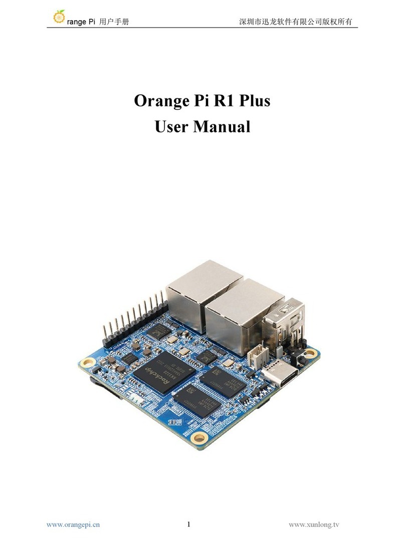
The AOP-12d is a PC-compatible short card which provides digital inputs and
outputs, and analogue outputs.
There are 24 TTL compatible programmable digital input/outputs available
externally. There are also three programmable timers. One of the timer outputs
is available externally to the user.
There are 12 analogue outputs available as ±10 Volts. Output resolution is
12 bits.
DMA data transfer is available on the analogue output channels.

Page 2Specification
Page 201270146.doc Blue Chip Technology Ltd.
SPECIFICATION
Analogue Outputs
Analogue Outputs 12 channels
Resolution 12 Bit Monotonic
Voltage Outputs ±10 Volts @ 10mA maximum one O/P,
or 5mA each from all O/Ps
Output Error Volts 0.5% of Span
Output Settling Time 3µS to ±1 LSB
Data Transfer I/O Port or DMA
DMA Channels Supported 1,2 and 3
Fastest DMA Transfer Rate 12µS per Transfer
Channel Selection Any or all channels may be selected to
be updated
DMA Transfer Initialisation Software Start Signal
Maximum Time Skew
Channel 1 To Channel 12 144µS
Between Channels 12µS
DMA Timing Source On-board Programmable Timer

Specification Page 3
Blue Chip Technology Ltd. 01270146.doc Page 3
Digital Input/Outputs
Number of Channels 24
Digital Inputs
High Level Input 2.2 Volts minimum
Current 10µA sink
Low Level Input 0.8 Volts maximum
Current 10µA source
Digital Outputs
Logic High Voltage 3.5 Volt minimum
Current 400µA source
Logic Low Voltage 0.4 Volt
Current 2.5mA sink

Page 4Specification
Page 401270146.doc Blue Chip Technology Ltd.
Timers
Number Of Timer Channels 3
Timer Usage
Timer 0 Pre-Scalar for timer 1
Timer 1 Timer for DMA transfer
Timer 2 Uncommitted (output available)
Timer 0
Resolution 1µS
Minimum Time 2µS
Maximum Time 130mS
Timer 1
Resolution timer 0 output value
Minimum Time 4µS
Maximum Time 2.3 hours
Timer 2
Resolution 1µS
Minimum Time 2µS
Maximum Time 130mS
Board Connectors
PC ISA 8-bit card
Analogue Signals 50 Way Male `D' Type
Digital Signals 50 Way IDC Male Box Header

Specification Page 5
Blue Chip Technology Ltd. 01270146.doc Page 5
ELECTROMAGNETIC COMPATIBILITY (EMC)
This product meets the requirements of the European EMC Directive
(89/336/EEC) and is eligible to bear the CE mark.
It has been assessed operating in a Blue Chip Technology Icon industrial PC.
However, because the board can be installed in a variety of computers, certain
conditions have to be applied to ensure that the compatibility is maintained. It
meets the requirements for an industrial environment ( Class A product) subject
to those conditions.
• The board must be installed in a computer system which provides screening
suitable for the industrial environment.
• Any recommendations made by the computer system manufacturer/supplier
must be complied with regarding earthing and the installation of boards.
• The board must be installed with the backplate securely screwed to the
chassis of the computer to ensure good metal-to-metal (i.e. earth) contact.
• Most EMC problems are caused by the external cabling to boards. With
analogue boards particular attention must be paid to this aspect. It is
imperative that any external cabling to the board is totally screened, and that
the screen of the cable connects to the metal end bracket of the board and
hence to earth. It is recommended that round screened cables with a braided
wire screen are used in preference to those with a foil screen and drain wire.
Use metal connector shells which connect around the full circumference of
the screen; they are far superior to those which earth the screen by a simple
“pig-tail”. Standard ribbon cable will not be adequate unless it is contained
wholly within the cabinetry housing the industrial PC.

Page 6Specification
Page 601270146.doc Blue Chip Technology Ltd.
• If difficulty with interference is experienced the cable should also be fitted
with a ferrite clamp as close possible to the connector. The preferred type is
the Chomerics clip-on style, type H8FE-1004-AS.
• It is recommended that cables are kept as short as possible, particularly
when dealing with low level signals.
• Ensure that the screen of the external cable is bonded to a good RF earth at
the remote end of the cable.
Failure to observe these recommendations may invalidate the EMC compliance.
Warning
This is a Class A product. In a domestic environment this product
may cause radio interference in which case the user may be required
to take adequate measures.
EMC Specification
A Blue Chip Technology Icon industrial PC fitted with this card meets the
following specification:
Emissions EN 55022:1995
Radiated Class A
Conducted Class A & B
Immunity EN 50082-1:1992 incorporating:
Electrostatic Discharge IEC 801-2:1984
Performance Criteria B
Radio Frequency Susceptibility IEC 801-3:1984
Performance Criteria A
Fast Burst Transients IEC 801-4:1988
Performance Criteria B

Quick Installation Page 7
Blue Chip Technology Ltd. 01270146.doc Page 7
QUICK INSTALLATION
Before installing the card into your computer system, there are a number of
links which must be set.
The settings of these links will depend upon the computer system into which the
card is being fitted. Users unfamiliar with the settings of links should refer to
the section “Detailed Card Installation”. For those unfamiliar with Binary and
Hexadecimal numbers, a brief explanation is included in the Appendices.
Base Address
Select an unused I/O address range for the card. The card requires a block of
16 contiguous addresses.
The base address is set on jumper block JP3. Fitting a link is equivalent to a
logic “0”. Leaving the link open is equivalent to a logic “1”. The card is
shipped with the default address setting of 300 Hex. This is suitable for most
small installations.
Interrupts
The DAC generates interrupts at the end of a DMA transfer. Interrupts IRQ2 to
IRQ7 are provided. The PIO and the Timer cannot generate interrupts.
The interrupt setting is selected by a link on jumper block JP1. If interrupt
operation is not required leave the link off.

Page 8Quick Installation
Page 801270146.doc Blue Chip Technology Ltd.
DMA Settings
The card can transfer data from memory to the analogue outputs using DMA.
The settings are controlled by links on jumper blocks JP2 and JP4. DMA
channels 1 and 3 are provided.
JP4 controls the setting of the DMA Request channels for the DAC. JP2
controls the setting of the DMA Acknowledge channels. The settings must be
the same on both JP2 and JP4. If DMA operation is not required, the links may
left open to allow the unused channels to be used by other cards.
The appendix contains a section explaining the use of DMA
Fitting the Card
Once all the links have been set, the card can be installed into the host
computer.
Observe all safety precautions and anti-static precautions. If possible try and
locate the card away from 'noisy' cards such as hard disc controllers, network
cards and processor cards.

Using the Card Page 9
Blue Chip Technology Ltd. 01270146.doc Page 9
USING THE CARD
External Input/Output Connections
The AOP-12d has two connectors for external circuitry.
The analogue output signals are available at a standard 50 pin D-type connector
which protrudes through the end bracket of the printed circuit board.
The digital input output signals are presented on a 50 way IDC header at the
inner end of the printed circuit board. These signals may be brought to a
connector on a second bracket the rear cover of the PC using a 50 way ribbon
extension cable. Filtered connectors are recommended for EMC.
Analogue Connections
The following table shows the pin out of the D-type analogue connector CON1.
The pins are arranged in three rows.
PIN USAGE PIN USAGE PIN USAGE
1V output 1 18 No connect 34 V output 12
2No connect 19 V output 7 35 No connect
3No connect 20 No connect 36 No connect
4V output 2 21 No connect 37 No connect
5No connect 22 V output 8 38 No connect
6No connect 23 No connect 39 No connect
7V output 3 24 No connect 40 No connect
8No connect 25 V output 9 41 No connect
9No connect 26 No connect 42 No connect
10 V output 4 27 No connect 43 No connect
11 No connect 28 V output 10 44 No connect
12 No connect 29 No connect 45 No connect
13 V output 5 30 No connect 46 No connect
14 No connect 31 V output 11 47 No connect
15 No connect 32 No connect 48 No connect
16 V output 6 33 No connect 49 Analogue ground
17 No connect 50 No connect

Page 10 Using the Card
Page 10 01270146.doc Blue Chip Technology Ltd.
Analogue Voltage Outputs
The analogue output signals from the AOP-12d are available as voltages only,
with the ability to supply a limited current.
Each of the 12 output signals (Voutput-1 to Voutput-12) has a corresponding
analogue ground or 0 Volt connection. The voltage outputs are referenced to
these connections. Measuring output voltages with reference to other ground
points (particularly the digital ground) will give electrically noisy results.
The voltage output has a span from +10 Volts to -10 Volts with an output drive
of 10mA maximum for any single output and 5mA maximum each for all
outputs simultaneously.
If large capacitive loads are to be connected to the voltage output, it is
recommended that a series resistance of approximately 100 ohms is placed in
series with the output voltage to avoid oscillations occurring at the output.

Using the Card Page 11
Blue Chip Technology Ltd. 01270146.doc Page 11
Digital Connections
The following table shows the pin out of the IDC digital signal connector
CON2. The pins are arranged in two rows.
PIN SIGNAL PIN SIGNAL
1DIO port A, bit 0 2DIO port A, bit 1
3DIO port A, bit 2 4DIO port A, bit 3
5DIO port A, bit 4 6DIO port A, bit 5
7DIO port A, bit 6 8DIO port A, bit 7
9DIO port B, bit 0 10 DIO port B, bit 1
11 DIO port B, bit 2 12 DIO port B, bit 3
13 DIO port B, bit 4 14 DIO port B, bit 5
15 DIO port B, bit 6 16 DIO port B, bit 7
17 DIO port C, bit 0 18 DIO port C, bit 1
19 DIO port C, bit 2 20 DIO port C, bit 3
21 DIO port C, bit 4 22 DIO port C, bit 5
23 DIO port C, bit 6 24 DIO port C, bit 7
25 Digital ground 26 Digital ground
27 Digital ground 28 Digital ground
29 Digital ground 30 Digital ground
31 Timer2 Output 32 Timer 0 Output
33 Digital ground 34 Digital ground
35 Digital ground 36 Digital ground
37 Digital ground 38 Digital ground
39 Digital ground 40 Digital ground
41 Digital ground 42 Digital ground
43 Digital ground 44 Digital ground
45 Digital ground 46 Digital ground
47 Digital ground 48 Digital ground
49 Digital ground 50 Digital ground
DIO - Digital input/output.

Page 12 Operation of the Card
Page 12 01270146.doc Blue Chip Technology Ltd.
OPERATION OF THE CARD
Programmable Digital Input/Outputs
The AOP-12d includes an NEC µPD71055 device which is equivalent to an
Intel 8255 PIO.
This device provides 24 programmable digital I/O channels. It is suitable for
sensing the presence of, or driving TTL connections only. These connections
should be kept as short as possible, less than 2 metres is recommended.
The digital I/O appears to the PC as four ports. The first three can be set as
input or output by writing suitable codes to the fourth Control Port.
These four ports are mapped into the AOP-12d address map as follows:
BASE
+ 4 Programmable Digital I/O Port A (read/write);
+ 5 Programmable Digital I/O Port B (read/write);
+ 6 Programmable Digital I/O Port C (read/write);
+ 7 Control Port (write only).
A summary of the codes required to change the operation of the ports are given
later. A typical sequence of events to use this feature would be :
• Decide on the input/output mix and write the appropriate code to
BASE + 7.
• Read from the selected output port or write to the selected output port.

Operation of The Card Page 13
Blue Chip Technology Ltd. 01270146.doc Page 13
Control Codes
The µPD71055 can operate in one of 3 modes.
The first (Mode 0) provides for simple inputs and outputs for three, 8 bit ports.
Data is written to or read from a specified port (A, B, or C) without the use of
handshaking.
The following table gives a summary of the most commonly used ‘Control
Words’ which must be written to the control port to configure the µPD71055
I/O ports in Mode 0.
CONTROL
WORD
(hex)
CONTROL
WORD
(decimal)
SET ALL
of PORT
A as
SET ALL
of PORT
B as
SET HIGH
4 BITS of
C as
SET LOW
4 BITS of
C as
80 128 Output Output Output Output
81 129 Output Output Output Input
82 130 Output Input Output Output
83 131 Output Input Output Input
88 136 Output Output Input Output
89 137 Output Output Input Input
8A 138 Output Input Input Output
8B 139 Output Input Input Input
90 144 Input Output Output Output
91 145 Input Output Output Input
92 146 Input Input Output Output
93 147 Input Input Output Input
98 152 Input Output Input Output
99 153 Input Output Input Input
9A 154 Input Input Input Output
9B 155 Input Input Input Input
Mode 1 enables the transfer of data to or from a specified 8 bit port (A or B) in
conjunction with strobes or handshaking signals on port C.
In Mode 2, data is transferred via one bi-directional 8 bit port (A) with
handshaking (port C).
Refer to the µPD71055 or i8255 data sheet for full details of the settings and use
of Modes 1 and 2.

Page 14 Operation of the Card
Page 14 01270146.doc Blue Chip Technology Ltd.
Timers
The AOP-12d includes an NEC µPD71054 timer chip which is equivalent to an
Intel 8254.
The timer chip contains three independent 16 bit counters which may be
operated in different modes. There are five basic modes of operation with each
mode providing a different output signal from the three output pins of the
device.
IMPORTANT
Timers 0 and 1 are crucial to the operation of the board. The DAC
section is controlled by the output of these timers so for all operating
modes of the DAC, these timers must be configured to run. See the
section on TIMER INITIALISATION for code examples to configure
these timers.
The reference clock for timers 0 and 2 is 1Mhz. Timer 1 is in series with the
output of timer 0.
Timer 0 is committed as the first divider for DMA in the AOP-12d and its
output is also available on the external connector.
Timer 2 is uncommitted in the AOP-12d and its output is available on the
external connector.
In DMA mode, timers 0 and 1 set the rate at which data is DMA’d. To set a
particular DMA rate, use the following equation:
Note that the 1 MHz clock is divided by 8 by the circuitry giving
a reference of 125 KHz
DMA RATE (in Hz) = 1250000 / divider
where “divider” = (65536 * TIMER 1 value) + (TIMER 0 value)
Table of contents
Other BlueChip Computer Hardware manuals
Popular Computer Hardware manuals by other brands
Electro-Voice
Electro-Voice FIR-DRIVE DX46 Specifications

Tri-M Systems
Tri-M Systems REB 2000 Series Faq

Kollmorgen
Kollmorgen SERVOSTAR S300 Technical description

Pico Macom
Pico Macom MOR-CS Installation and operation manual

Delta Electronics
Delta Electronics Suppression Inductors LFZ24H Specification sheet

Manhattan
Manhattan 150583 user manual