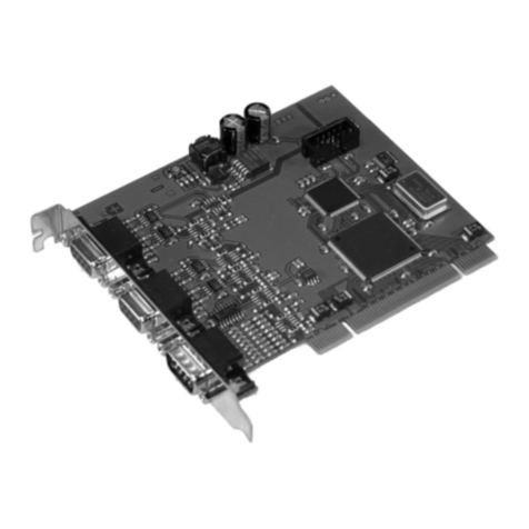
ComputerBoards, Inc PCI-DAS4020/12 User manual

PCI-DAS4020/12
User’s Manual
ComputerBoards, Inc.
Revision 1, April, 2000
© Copyright 2000

ii
NO PART OF THIS MANUAL MAY BE REPRODUCED IN ANY FORM WITHOUT WRITTEN
PERMISSION FROM COMPUTERBOARDS, INC.
All rights reserved. No part of this publication may be reproduced, stored in a retrieval system, or
transmitted, in any form by any means, electronic, mechanical, by photocopying, recording or otherwise
without the prior written permission of ComputerBoards, Inc.
MEGA-FIFO, the CIO prefix to data acquisition board model numbers, the PCM prefix to data
acquisition board model numbers, PCM-DAS08, PCM-D24C3, PCM-DAC02, PCM-COM422, PCM-
COM485, PCM-DMM, PCM-DAS16D/12, PCM-DAS16S/12, PCM-DAS16D/16, PCM-DAS16S/16,
PCI-DAS6402/16, Universal Library,InstaCal, Harsh Environment Warranty and ComputerBoards are
registered trademarks of ComputerBoards, Inc.
IBM, PC, and PC/AT are trademarks of International Business Machines Corp.
Windows is a trademark of Microsoft Corp.
Information furnished by ComputerBoards, Inc. is believed to be accurate and reliable. However, no
responsibility is assumed by ComputerBoards, Inc. neither for its use; nor for any infringements of
patents or other rights of third parties, which may result from its use. No license is granted by implication
or otherwise under any patent or copyrights of ComputerBoards, Inc.
Notice
ComputerBoards, Inc. does not authorize any ComputerBoards, Inc.
product for use in life support systems and/or devices without the written
approval of the President of ComputerBoards, Inc. Life support
devices/systems are devices or systems which, a) are intended for surgical
implantation into the body, or b) support or sustain life and whose failure
to perform can be reasonably expected to result in injury.
ComputerBoards, Inc. products are not designed with the components
required, and are not subject to the testing required to ensure a level of
reliability suitable for the treatment and diagnosis of people.
HM PCI-DAS4020/12.DOC
iii
Table of Contents
1. INTRODUCTION AND PRODUCT DESCRIPTION....................................................................... 1
1.1 INTRODUCTION.................................................................................................................................... 1
1.2 ANALOG SIGNAL PATH ....................................................................................................................... 2
1.3 ANALOG OUTPUT SECTION......................................................................................................... 2
1.4 ANALOG OUTPUT SECTION - BLOCK DIAGRAM (FIGURE 1-2) ............................................. 3
1.5 DIGITAL I/O SECTION .................................................................................................................... 3
1.6 POWER DISTRIBUTION SECTION................................................................................................ 3
2. INSTALLATION.................................................................................................................................... 4
3. CONNECTIONS .................................................................................................................................... 5
4. PROGRAMMING AND APPLICATIONS......................................................................................... 7
4.1 PROGRAMMING LANGUAGES .............................................................................................................. 7
4.2 PACKAGED APPLICATIONS PROGRAMS............................................................................................... 7
5. REGISTER DESCRIPTION.................................................................................................................8
5.1 PCI-DAS4020/12 MEMORY MAP ....................................................................................................... 8
5.2 LOCALSPACE0 WRITE-ONLY REGISTERS............................................................................................ 9
5.3 LOCALSPACE0 READ-ONLY REGISTERS ............................................................................................. 9
5.4 LOCALSPACE0 READ/WRITE REGISTERS............................................................................................ 9
5.4.1 LocalSpace0 Read/Write Registers............................................................................................ 10
5.4.2 LocalSpace0 Serial Devices....................................................................................................... 10
5.4.3 Register Descriptions – Detailed................................................................................................ 10
5.4.4 LocalSpace0 Write-only Registers............................................................................................. 10
5.4.5 I2C INTERFACE:...................................................................................................................... 21
6. INITIATING A/D CONVERSIONS...................................................................................................23
6.1 DEFINITIONS AND IMPLEMENTATION................................................................................................ 23
6.2 INITIATING CONVERSION VIA THE BNC CONNECTION: RELATED PIN DESCRIPTIONS..................... 24
6.3 INITIATING CONVERSION VIA ANALOG INPUT BNC CONNECTIONS:................................................. 24
7. CALIBRATION.................................................................................................................................... 25
CALIBRATING THE PCI-DAC4020/12..................................................................................................... 25
8. SPECIFICATIONS.............................................................................................................................. 26

iv
This page is blank.

1
1. INTRODUCTION AND PRODUCT DESCRIPTION
1.1 INTRODUCTION
The PCI-DAS4020/12 (Figure 1-1) is a multi-function I/O board. It consists of the following:
1. Four high-speed analog input channels. Each channel can be configured by software for an input
range of +/-1V or +/-5V. Resolution is 12 bits. Throughput is 10 to 20 MHz depending on the number
of channels accessed. Triggering sources are by hardware or software, internal or external, and four
different modes are software selectable. A/D gating is likewise by either hardware or software,
internal or external. Input connectors are BNC types. Refer to the specifications in this manual for full
details.
2. Two analog output channels. Each channel can be configured by software for an output range of
+/-10V or +/-5V. Resolution is 12 bits. Throughput is system-dependent. Triggering mode is software
gate. D/A pacing is software. Refer to the specifications in this manual for full details.
3. Twenty-four digital I/O channels. The I/O chip type is 82C55A configured as two banks of eight and
two banks of four, programmable by bank as input or output. Signal levels are TTL. The digital I/O
and analog out connector is a 40-pin header.
BNC
BNC
INPUT
MUX
GAIN & OFFSET
AUTOCAL
ADC
IN
SYSTEM
TIMING
CONTROLLER
DUAL
32Kx24
SRAM
PC BUS
CONTROLLER
USER
DUAL 12-BIT
DACs
USER
DIGITAL I/0
(8255)
PCI BUS CONNECTOR
(5V, 32 BIT, 33 MHZ)
VREF
CONV
ATTENUATOR/
AMPLIFIER
ANALOG
CLOCK/
TRIGGER
LOCAL BUS
EXTERNAL PACER,
TRIG1, TRIG2,
or GATE
FOUR ANALOG INPUT CHANNELS PER BOARD
50 Ohm
ANALOG
OUTPUTS
24 I/O
FOUR
CHANNELS
12
Figure 1-1. PCI-DAS4020/12 Block Diagram

2
1.2 ANALOG SIGNAL PATH
Four single-ended analog input channels connect from BNC connectors to individual amplifiers, then to
dedicated ADC’s. Each path allows for:
•50 ohm or high-Z termination, selected by solder gap;
•+/-1V or +/-5V bipolar ranges, software-selectable (Table 1-1);
•Auto-calibration for offset and gain adjustments for each channel and each range.
Table 1-1. Input Range
FULL SCALE
INPUT RANGE ATTENUATION DIVIDER
OUTPUT
+5V to -5V 5 +/-1V
+1V to -1V 1 +/-1V
1.3 ANALOG OUTPUT SECTION
Two 12-bit voltage outputs are software programmable for +/- 10V or +/- 5V. The D/A is the Analog
Devices AD7237 Dual DAC. Since the DAC is dual buffered, the DAC output voltage is updated after the
MS nibble is written to the DAC.
The DACs initially power-up and are reset to 0V.
There is no calibration on these DACs. The offset and gain errors are minimized by using precision
components in Table 1-2 shows the DAC input coding.
Table 1-2. DAC Input Coding
DAC
RANGE INPUT CODE
BINARY 12 BIT INPUT
CODE HEX 12 BIT OUTPUT
VOLTAGE
+/- 10V 0000 0000 0000 000h −10.000 V
+/- 10V 1000 0000 0000 800h 0 V
+/- 10V 1111 1111 1111 FFFh +9.99513 V
+/- 5V 0000 0000 0000 000h −5.000 V
+/- 5V 1000 0000 0000 800h 0 V
+/- 5V 1111 1111 1111 FFFh +4.99756 V

3
1.4 ANALOG OUTPUT SECTION - BLOCK DIAGRAM (FIGURE 1-2)
Figure 1-2. Analog Output Block Diagram
1.5 DIGITAL I/O SECTION
The digital I/O is comprised of an 82C55 digital logic device. The pinout is identical to the auxiliary
DIO24 on a 40-pin header (P3).
For external interrupts, an external interrupt source pin and external interrupt enable pin are provided on
connector P3. These lines are pulled up and OR’ed to generate the external interrupt signal. Both are
active low.
1.6 POWER DISTRIBUTION SECTION
Power for the board is from the PCI bus. The only power used is +5V.
Range Select
AD7237
Dual DAC DAC0
DAC1
VDAC0
VDAC1
Precision
Summing Amps
To Auxiliary
connector and
Analog Trigger
circuit

4
2. INSTALLATION
The PCI-DAS4020/12 is completely plug and play. There are no switches or jumpers to set.
Configuration is controlled by your systems’ BIOS. Simply turn off your PC, open it up and insert the
PCI-DAS4020/12 into any available PCI slot.
If you are using an operating system with support for Plug and Play (such as Windows 95 or 98), a dialog
box will pop up as the system loads indicating that new hardware was detected. If the information file for
this board is not already loaded onto your PC, you are prompted for a disk containing it. The InstaCal™
software supplied with your board contains this file. Just insert the disk or CD and click OK.
To easily test your installation, install InstaCal, the installation, calibration, and test utility supplied with
your board. Refer to the Software Installation Manual for information on the initial setup, loading, and
installation of InstaCal and optional universal library™ software.

5
3. CONNECTIONS
Figure 3-1 shows the pinout for the 40-pin connector. Figure 3-2 shows the Analog Inputs and Trigger In
BNC connectors.
I_XINT* 1
XINT_EN* 3
PB7 5
PB6 7
PB5 9
PB4 11
PB3 13
PB2 15
PB1 17
PB0 19
GND 21
NC 23
GND 25
NC 27
GND 29
NC 31
GND 33
+5V 35
GND 37
VDAC0 39
2 +5V
4 GND
6 PC7 (IAIGATE)
8 PC6 (ITRIG2)
10 PC5 (ITRIG1/EXT CLK)
12 PC4
14 PC3
16 PC2
18 PC1
20 PC0
22 PA7
24 PA6
26 PA5
28 PA4
30 PA3
32 PA2
34 PA1
36 PA0
38 VDAC RETURN
40 VDAC1
PCI-DAS4020/12 Connector Diagram
*PINS1&3HAVE10KPULL-UP RESISTORS INSTALLED.
P3
Figure 3-1. 40-Pin Connector
NOTE: When using analog outputs VDAC0 and VDAC1, use VDAC RETURN only (pin 38) for the
return.

6
View from rear of the PC.
Channel 0
Channel 1
Channel 2
Channel 3
Trigger Input
Figure 3-2. Analog Inputs and Trigger Input BNC Connectors

7
4. PROGRAMMING AND APPLICATIONS
After following the installation instructions, your PCI-DAS4020/12 is ready for use. Although the board
is part of the larger DAS family, there is no correspondence between registers. Software written at the
register level for other DAS models will not work with the PCI-DAS4020/12.
4.1 PROGRAMMING LANGUAGES
The ComputerBoards Universal Library™ provides complete access to the PCI-DAS4020/12 functions
from a variety of Windows programming languages. If you are planning to write programs, or would like
to run the example programs for Visual Basic or any other language, please refer to the Universal Library
manual.
VIX Components is a set of programming tools based on a DLL interface to Windows languages. A set of
VBX, OCX or ActiveX interfaces allows point-and-click construction of graphical displays, analysis and
control structures. Please refer to the catalog for a complete description of the package.
4.2 PACKAGED APPLICATIONS PROGRAMS
Many packaged application programs, such as DAS-Wizard™, Labtech Notebook™, and HP-VEE™,
now have drivers for the PCI-DAS4020/12. If the package you own does not appear to have drivers for
the board, please fax or e-mail the package name and the revision number from the install disks. We will
research the package for you and advise how to obtain PCI-DAS4020/12 drivers.
Some application drivers are included with the Universal Library package, but not with the Application
package. If you have purchased an application package directly from the software vendor, you may need
to purchase our Universal Library and drivers. Please contact us for more information on this topic.

8
5. REGISTER DESCRIPTION
5.1 PCI-DAS4020/12 MEMORY MAP
Table 5-1 lists PCI Base Address Assignments.
Table 5-1. PCI Base Address Assignments
Memory Region Function Operations
BAR0 PLX 9080 PCI controller operation registers 32-bit DWORD
BAR2 PCI-DAS4020/12 16-bit registers 16-bit WORD
BAR3 PCI-DAS4020/12 FIFO 32-bit DWORD
Any operations to the PLX 9080 PCI controller registers at BAR0 require a thorough understanding of the
9080 chip specification. Detailed descriptions of 9080 operation are beyond the scope of this document.
The interested reader is encouraged to obtain the “PLX New Products Catalog, February 1998” for
detailed programming information.
The PLX 9080 provides internal address decoding which allows remapping of BAR2 and BAR3 to
convenient Local Address values. This eases the burden of Local Bus address decoding. The remap and
space-specific parameters for the PCI-DAS4020/12 are summarized in Table 5-2 below:
Table 5-2. Address Remap
PCI BAR Space Width Burst Enabled Size Remap Address
BAR2 Registers 16 N 4K 0x0000 2000
BAR3 FIFOs 32 Y 4K 0x0000 3000
NOTE: Unless otherwise specified, the remapped version of BAR2 is referred to as LocalSpace0
while the remap of BAR3 will be referred to as LocalSpace1.Register Summary

9
5.2 LOCALSPACE0 WRITE-ONLY REGISTERS
Table 5-3 summarizes the LocalSpace0 write-only registers (16-bit).
Table 5-3. LocalSpace0 Write-Only Registers
Register Group Register Name Offset Address
Configuration Group Interrupt Enable Register 0x00
Hardware Configuration Register 0x02
Memory Size Register 0x04
ADC Register Group ATRIG LOW Register 0x0C
ATRIG HIGH register 0x0E
Control Register 0 0x10
Control Register 1 0x12
Sample Interval Register (LOW) 0x16
Sample Interval Register (HIGH) 0x18
Sample/Scan Count Register (LOW) 0x1E
Sample/Scan Count Register (HIGH) 0x20
DAQ Soft Start Command 0x22
DAQ Single Conversion Command 0x24
ADC FIFO pointer clear command 0x2A
DAC Register Group DAC Control Register 1 0x52
DAC0 Single Conversion Command (LSB) 0x70
DAC0 Single Conversion Command (MSB) 0x72
DAC1 Single Conversion Command (LSB) 0x74
DAC1 Single Conversion Command (MSB) 0x76
5.3 LOCALSPACE0 READ-ONLY REGISTERS
Table 5-4 summarizes the LocalSpace0 read-only registers (16-bit).
Table 5-4. LocalSpace0 Read-Only Registers
Register Name Offset Address
Hardware Status Register 0x00
ADC Read Pointer Register 0x08
ADC Write Pointer Register 0x0C
User XFER Counter Register (LOW) 0x10
Pre/Post Register 0x14
User Chip Select 1 0x48:4E
5.4 LOCALSPACE0 READ/WRITE REGISTERS
Table 5-5 summarizes the LocalSpace0 read/write registers (16-bit):
Table 5-5. LocalSpace0 Read/Write Registers
Register Group Register Name Offset Address
Primary Digital I/O (8255) Digital Port A 0x48
Digital Port B 0x4A
Digital Port C 0x4C
Digital Port Control 0x4E

10
5.4.1 LocalSpace0 Read/Write Registers
Table 5-6 identifies the LocalSpace0 read/write register (32-bit):
Table 5-6. LocalSpace0 Read/Write Register
Register Name Offset Address
ADC XFIFO 0x200
5.4.2 LocalSpace0 Serial Devices
Table 5-7 summarizes the LocalSpace0 write-only serial devices:
Table 5-7. LocalSpace0 Write-Only Serial Devices
I2C Device Address
I2C Register 0x40
CAL DAC0 0x18
CAL DAC1 0x1A
5.4.3 Register Descriptions – Detailed
This section provides detailed descriptions of all LocalSpace0 registers. Note that the DAQ refers to
analog-input data acquisition while DAC refers to analog output operations. Bit locations that are hard-
coded with either (0) or a (1) must be written with these values during register accesses.
5.4.4 LocalSpace0 Write-only Registers
Configuration Group
Interrupt Enable Register
15 14 13 12 11 10 9 8
OVERRUN DAQ_STOP DAQ_ACTIVE XINT
MSB
76 5 4 3 2 1 0
DAQDONE DAQ_IENB 0 DAQ_ISRC0
LSB

11
Bit Name Description
15 OVERRUN DAQ Overrun Enable – If this bit is set, a DAQ overrun condition can be detected. DAQ
overrun does not cause an interrupt but does set a bit in the Status register.
10 DAQ_STOP DAQ STOP Interrupt Enable – If this bit is set, an interrupt is generated when the stop
trigger (TRIG2) is detected.
9 DAQ_ACTIVE DAQ ACTIVE Interrupt Enable – If this bit is set, an interrupt is generated when a DAQ
sequence is active.
8 XINT XINT Interrupt Enable – If this bit is set, the external XINT signal can generate an
interrupt.
3 DAQDONE DAQDONE Interrupt Enable – If this bit is set, an interrupt is generated when the DAQ
sequence completes. A DAQ sequence ends by running its course or when an OVERRUN
condition occurs.
2 DAQ_IENB DAQ Interrupt Enable – If this bit is set, one of the DAQ_ISRC conditions generates an
interrupt.
0 DAQ_ISRC0 DAQ Interrupt Source select – This bit is used to select an additional DAQ interrupt
source, in addition to the DAQDONE source.
DAQ_ISRC0 Description
0 DAQ FIFO ¼ Full
1 DAQ Single Conversion: An interrupt is generated each conversion.
Single Conversion Command: An interrupt can be generated for each ADC conversion when the
corresponding ADC data is available in the AFIFO.
Paced Conversions: An interrupt can be generated each ADC conversion during paced conversions
when the corresponding ADC data is available in the AFIFO. The following restrictions apply to
this mode:
1. For single-channel paced conversions, place the STC in 2-Channel mode via DAQ Control 1
register.
2. Set the DSBL_DMA bit via the DAQ Control 0 register.
3. After the interrupt has been received, issue an ADC FIFO pointer clear command to permit
data to be retrieved form the FIFO.
Hardware Configuration Register
15 14 13 12 11 10 9 8
XINT_POL
MSB
765432 1 0
0 0 0 0 0 0 WCLK_SRC1 WCLK_SRC0
LSB

12
Bit Name Description
8 XINT_POL External Interrupt (XINT) polarity select: 0 = rising edge sensitive; 1 = falling edge
sensitive.
1-0 WCLK_SRC(1:0) PACER Base Clock Source:
WCLK_SRC1 WCLK_SRC0 Description
00Inactive
0 1 On Card 40MHz oscillator
1 0 Analog Clock
1 1 Digital TRIG1 pin
Memory Size Register
15 14 13 12 11 10 9 8
7654321 0
ASEG6 ASEG5 ASEG4 ASEG3 ASEG2 ASEG1 ASEG0
LSB
Bit Name Description
6-0 ASEG(6:0) ADC buffer segment size (FIFO size): The FIFO size can range from 256 samples deep
upward to 32K samples deep, in increments of 256 samples. Note that the FIFO is actually 24
bits wide; therefore, two samples can be stored per FIFO location.
ASEG(6:0) FIFO size In sample
7F 256 512
7E 512 1K
7C 1K 2K
78 2K 4K
70 4K 8K
60 8K 16K
40 16K 32K
00 32K 64K
Note: There are actually two FIFO banks (X and Y) populated on the board. Each bank can provide 64K
samples. In Burst mode the total FIFO size maximum is 2 x 64K = 128K samples.

13
DAQ ATRIG LOW Register
15 14 13 12 11 10 9 8
XAGATE_SRC XTRIG2_SRC XTRIG1_SRC THRESH_L11 THRESH_L10 THRESH_L9 THRESH_L8
MSB
76543 210
THRESH_L7 THRESH_L6 THRESH_L5 THRESH_L4 THRESH_L3 THRESH_L2 THRESH_L1 THRESH_L0
LSB
15 XTRIG1_SRC External TRIG1 Source select: 0 = TRIG1 pin; 1 = BNC source. The External
XTRIG1 Mode bit in the DAQ Control Register 0 must be set for this bit to be used.
14 XTRIG2_SRC External TRIG2 Source select: 0 = TRIG2 pin; 1 = BNC source. The External
XTRIG1 Mode bit in the DAQ Control Register 0 must be set for this bit to be used.
13 XAGATE_SRC External AGATE Source select: 0 = AGATE pin; 1 = BNC source
12-2 THRESH_L(11:0) Threshold Low Value: This register is used to load the LOW threshold value for
Analog triggering.
DAQ ATRIG HIGH Register
15 14 13 12 11 10 9 8
THRESH_H11 THRESH_H10 THRESH_H9 THRESH_H8
MSB
76543210
THRESH_H7 THRESH_H6 THRESH_H5 THRESH_H4 THRESH_H3 THRESH_H2 THRESH_H1 THRESH_H0
LSB
12-2 THRESH_H(11:0) Threshold High Value: This register is used to load the HIGH threshold value for
Analog triggering.
DAQ Control Register 0
15 14 13 12 11 10 9 8
DAQ_ENB DMA_DSBL GATE_SEQ SAMPCNT ENB XCONV_POL TRIG2_ENB TRIG2_POL
MSB
7654 32 1 0
TRIG2_SRC TRIG1_POL TRIG1_SRC1 TRIG1_SRC0 AGATE_POL AGATE_LVL AGATE_SRC1 AGATE_SRC0
LSB

14
Bit Name Description
15 DAQ_ENB Data Acquisition Enable – This bit enables and disables a data acquisition operation. It
is the master enable for DAQ operations.
14 DMA_DSBL DMA Disable; This bit should be cleared only when the STC device is transferring
data to the host via DEMAND MODE DMA. Refer to the PLX New Products catalog
for DEMAND MODE DMA details.
13 GATE_SEQ GATE ON Sequence: If this bit is set in multi-channel mode, an inactive gate will
pause the data acquisition after the current scan sequence has completed. If this bit is
cleared, an inactive gate pauses the data acquisition immediately.
12 SAMPCNT ENB Sample Counter Enable. When this bit is set, the DAQ Sample counter in enabled. This
bit must be set for pre/post triggered mode.
11 XCONV_POL External A/D Convert polarity control. This bit controls the polarity of the External
A/D convert input signal. If a low-to-high edge of XCONV is to be used to initiate a
conversion then this bit should be cleared. If a high-to-low edge of XCONV is to be
used to initiate a conversion then this bit should be set.
9 TRIG2_ENB TRIG2 pre-trigger Enable. This bit enables pre-trigger mode.
8 TRIG2_POL TRIG2 trigger polarity select: 0 = rising edge trigger; 1 = falling edge trigger.
7 TRIG2_SRC TRIG2 pre-trigger source select: 0 = External X_TRIG2 pin; 1 = Analog Trigger.
6 TRIG1_POL TRIG1 trigger polarity select: 0 = rising edge trigger; 1 = falling edge trigger.
5-4 TRIG1_SRC(1:0) TRIG1 Source select – These bits are used to select TRIG1 source.
TRIG1_SRC1 TRIG1_SRC0 DESCRIPTION
0 0 Disabled
01Soft_Trigger
1 0 External XTRIG1
1 1 Analog Trigger
3 AGATE_POL AGATE polarity select: 0 = active high gate; 1 = active low gate.
2 AGATE_LVL AGATE Level select; 0 = edge sensitive gate; 1 = level sensitive gate;
1-0 AGATE_SRC(1:0) AGATE Source select – These bits are used to select AGATE source.
AGATE_SRC1 AGATE_SRC0 DESCRIPTION
0 0 Disabled
0 1 Soft_Gate
1 0 External AGATE
1 1 Analog Gate
DAQ Control Register 1
15 14 13 12 11 10 9 8
PSC_ENB CHANMODE1 CHANMODE0 HCHANSEL1 HCHANSEL0 LCHANSEL1 LCHANSEL0
MSB
7654321 0
0 SFT_AGATE ATRIGSRC1 ATRIGSRC0 ATRIGMD2 ATRIGMD1 ATRIGMD0 LSB

15
Bit Name Description
15 PSC_ENB Pre-Scale Enable bit. If this bit is set then the WCLK is prescaled by 400. If the
WCLK Source is 40 MHz then the Pacer clock source is 40 MHZ/400 = 100 kHz.
13-12 CHANMODE(3:0) Channel MODE select bits.
CHANMODE1 CHANMODE0 MODE Comments
00Single
Channel 20MHZ max. sample rate
0 1 Two Channels 20MHZ max. sample rate
1 0 Four Channels 10MHZ max. sample rate
1 1 Four Channel
Transient 20MHZ max. sample rate; single burst
of 32K samples max per channel.
11-10 UCHANSEL(1:0) High Channel select bits. These bits are used to select the high channel in Two-
Channel mode.
HCHANSEL1 HCHANSEL0 Selected Channel
0 0 Channel A
0 1 Channel B
1 0 Channel C
1 1 Channel D
9-8 LCHANSEL(1:0) Low Channel select bits. These bits select the low channel in Two Channel mode.
LCHANSEL1 LCHANSEL0 Selected Channel
00 ChannelA
01 ChannelB
10 ChannelC
11 ChannelD
6 SFT_GATE Software DAQ Gate - When SFT_GATE is cleared, no A/D conversions take place. When
SFT_GATE is set, A/D conversions take place normally. SFT_GATE can be used as a
software gating tool, or to inhibit random conversions during setup operations.
5-4 ATRIGSRC(1:0) Analog Trigger Channel Source
ATRIGSRC1 ATRIGSRC0 Selected Channel
00 ChannelA
01 ChannelB
10 ChannelC
11 ChannelD
3-1 ATRIGMD(2:0) Analog Trigger/Gate Mode select bits.

16
Analog Trigger/Gate Modes
ATRIGMD2 ATRIGMD1 ATRIGMD0 Mode Description
0 0 0 INACTIVE Inactive state. Prior to programming the analog trigger to
the desired state, the analog trigger should be
programmed to the inactive state to clear out the trigger
circuitry.
0 1 0 Positive
Hysteresis The trigger is generated when the signal value is greater
than the high-value, with hysteresis specified by
low_value.
0 1 1 Negative
Hysteresis The trigger is generated when the signal value is greater
than the low-value, with hysteresis specified by
high_value.
1 0 0 Negative
Slope The trigger is generated when the signal value is less than
low-value.
1 0 1 Positive
Slope The trigger is generated when the signal value is greater
than high-value.
1 1 0 Window The trigger is generated when the signal value is between
the low-value and high-value.
ADC Sample Interval Register (Lower)
15 14 13 12 11 10 9 8
ADCSIL15 ADCSIL14 ADCSIL13 ADCSIL12 ADCSIL11 ADCSIL10 ADCSIL9 ADCSIL8
MSB
7654321 0
ADCSIL7 ADCSIL6 ADCSIL5 ADCSIL4 ADCSIL3 ADCSIL2 ADCSIL1 ADCSIL0
LSB
Bit Name Description
15-0 ADCSIL(15:0) ADC Sample Interval Lower - The lower 16 bits of the Sample Interval divisor.
ADC Sample Interval Register (Upper)
15 14 13 12 11 10 9 8
MSB
7654321 0
ADCSIL23 ADCSIL22 ADCSIL21 ADCSIL20 ADCSIL19 ADCSIL18 ADCSIL17 ADCSIL16
LSB
BIT Name Description
15-0 ADCSIL(23:16) ADC Sample Interval upper - The upper 8 bits of the Sample Interval divisor.
ADC Pacer Frequency = Base_clock/(Divider + 2)
ADC Sample/Scan Count Register (Lower)
15 14 13 12 11 10 9 8
ADCSMP15 ADCSMP14 ADCSMP13 ADCSMP12 ADCSMP11 ADCSMP10 ADCSMP9 ADCSMP8
MSB
765432 10
ADCSMP7 ADCSMP6 ADCSMP5 ADCSMP4 ADCSMP3 ADCSMP2 ADCSMP1 ADCSMP0
Table of contents