EnerPro FCRO4100 User manual

http://www.enerpro-inc.com
99 Aero Camino
Goleta, California 93117
Operating Manual: OP-0106
August 2019
Enerpro Document No: OP-0106, Rev. B Page 1 of 14 ECO #19-11089; Release Date: 08/02/2019
Operating Manual: Four-SCR General Purpose Gate Firing Board
FCRO4100 Revision L
Introduction
This manual describes the salient features and specifications of the FCRO4100 firing board, including
typical firing circuit signal waveforms and a checkout procedure.
Product Description
1.0 Application
The FCRO4100 board is a four-SCR firing board suitable for use with single-phase AC
controllers, center-tap or full wave rectifiers. The firing board responds to a voltage or current
delay angle command signal (SIG HI) to produce four delayed, isolated, 180°-spaced high-
current SCR gate firing pulses. An optional regulator circuit provides voltage or current regulation
and optional plug-in regulator boards provide voltage/current limiting or polarity transition
functionality for four-quadrant rectifiers.
2.0 ASIC-Based Firing Circuit
All firing circuit logic is contained in a custom 20-pin ASIC. Additional detail on the firing circuit
theory is contained in a separate engineering society paper1.
3.0 Board Mounted Connectors
3.1. Gate/Cathode and Control Power Connector
Six-position header J1 provides the connections for the +X1 SCR (load connected cathode) at
positions 1 and 2 and for the -X1 SCR (line connected cathode) at positions 5 and 6.
Five-position header J2 provides the connections for the +X2 SCR (load connected cathode) at
positions 1 and 2 and for the –X2 SCR (line connected cathode) at positions 4 and 5.
The board-mounted 24 VA power supply transformer (T1) is normally energized by connecting
the mains voltage at J3. The gate firing signals are locked to the mains waveform through the
power control transformer, hence, the board power must be in phase with the mains voltage.
3.2. Control Signal Connector
The delay angle command (SIG HI), instant and soft inhibit controls, voltage and current feedback
signal, and auxiliary power connections are available through J4, a 12-position Mate-N-Lok™
connector. The pinout of this connector is detailed in drawing E168 Rev L.
3.3. Feedback Signal Connector and Plug-In Regulator Board Connector
The FCRO4100 board can accept voltage and current feedback in certain configurations.
Ground-referenced voltage feedback and current limit command signals enter on J5 pins 4 and 5
respectively. Current feedback signals from CTs enter on J5 pins 1 and 2 and connect to the
associated bridge rectifier and burden resistor. A 14-position connector J6 provides an interface
for plug-in regulator boards; see section 7.0 for operational information regarding regulation
capabilities.
3.4. Auxiliary Firing Board Connector
Six-position MTA header J7 provides board power, circuit common, and SCR gate signals that
connect to the FCOAUX60 auxiliary firing board to provide four-quadrant operation. See section
6.0 for operational information regarding four-quadrant applications.
1 Bourbeau, F. J., “Phase Control Thyristor Firing Circuit: Theory and Applications”, Power Quality ’89, Long Beach, California.

Enerpro Document No: OP-0106, Rev. B Page 2 of 14 ECO #19-11089; Release Date: 08/02/2019
3.5. Operating Frequency Selection
The FCRO4100 board may be set for operation at 50 or 60 Hz by making the appropriate jumper
selection at J8. VCO timing resistor R12 is set by the factory; the addition or omission of R13 by
J8 ensures the correct closed-loop PLL response.
4.0 Gate Delay Command
The SIG HI delay angle command signal is inversely proportional to the delay angle. When SIG
HI is at a maximum, the delay angle is at a minimum value, corresponding to maximum rectifier or
controller output. When SIG HI is at a minimum, the delay angle is at a maximum value,
corresponding to a minimum rectifier or controller output.
The delay command signal, SIG HI, may be configured as a voltage (0 to 5 Vdc) or current signal.
When SIG HI is a current signal, R11 is selected to provide 5.0 Vdc at the maximum delay angle
command signal current, typically 249 ohms for a 4 to 20 mA or 0 to 20 mA range.
5.0 Bias and Span Potentiometers
Two 5.0 kΩ potentiometers are used to control the bias (R6) and span (R7) of the delay angle
command signal. These controls allow the customer to change the delay angle range for a
specific application. Note that the maximum effective full-scale delay angle command range is
limited to approximately 10° ≤ α ≤ 170°.
With the FCRO4100 board connected to the SCRs, set the SIG HI command to its minimum
value (above 0.5 Vdc if the low signal inhibit circuit is connected via D6). Enable firing and
observe that the inhibit LED, PD1, extinguishes. Adjust the BIAS potentiometer, R6, to achieve
the desired minimum output voltage or current. Increase SIG HI to its maximum value and adjust
the SPAN potentiometer, R7, to obtain the maximum desired output. Decrease SIG HI again to
the level used to set the bias potentiometer and check that the desired minimum output voltage or
current has remained the same after adjusting R7. If necessary, incrementally adjust R6 and R7
in this manner several times to achieve the required range.
Figure 1 shows the phase detector (TP6) waveforms for maximum delay angle (SIG HI = 0.5 V)
and minimum delay angle (SIG HI = 5.0 V). Calculate the delay angle from the duty cycle of the
waveform at TP6 as )1(180 D
. The approximate minimum duty cycle of D = 0.06 corresponds
to a maximum delay angle of 169)06.01(180
max
. The approximate maximum duty cycle of D
= 0.96 corresponds to a minimum delay angle of 180°(1-0.96) ≈ 7.2°
Figure 1. Maximum and Minimum Delay Angle Calculation
Channel 1: Phase Detector (TP6), SIG HI = 0.5 Vdc, D = 0.06, = 169°
Channel 2: Phase Detector (TP6), SIG HI = 5.0 Vdc, D = 0.96, = 7.2°

Enerpro Document No: OP-0106, Rev. B Page 3 of 14 ECO #19-11089; Release Date: 08/02/2019
6.0 Bipolar Operation
The FCRO4100 is capable of firing four-quadrant converters in two- or four-pulse configurations.
For two-quadrant two-pulse converters, install jumper JU1, omit jumper JU2, and leave the “Cut
Trace” indication on J4 positions 5 and 6 intact. In this configuration, connector J1 provides the
gating signals for the positive bridge and J2 provides the gating signals for the negative bridge.
For four-quadrant four-pulse converters the FCOAUX60 connects to the FCRO4100 and provides
an additional set of four isolated gate outputs. A cable connects the FCRO4100’s auxiliary gate
outputs on J7 to the gate inputs on the FCOAUX60’s J3 or J4 connector. On the FCRO4100
board, omit jumper JU1, install jumper JU2, and cut the trace where indicated between J4
positions 5 and 6. The positive bridge gating signals are provided by J1 and J2 on the FCRO4100
board and the negative bridge gating signals are provided by J1 and J2 on the FCOAUX60. The
P signal on J4 pin 5 controls the rectifier polarity. This signal is normally pulled to +12 V through
resistor RN4D (1.50 kΩ) which sets the rectifier output to the positive polarity. Grounding this
signal instantly reverses the rectifier polarity. For timed polarity transition, the PTIR-1 timed
polarity transition inhibit board provides approximately 100 ms of dead time (i.e., SCR firing is
inhibited for 100 ms) between polarity transition with an optional voltage regulation feature.
7.0 Regulator Circuit
The FCRO4100 board includes an optional regulation circuit for ac current feedback as supplied
by a current transformer. Burden resistor R4, connected to the output of bridge rectifier BR1, is
selected to provide 1.0 Vdc at the desired full load current or voltage.
The VRCL1P-1 regulator board (sold separately) extends the FCRO4100’s functionality by
providing voltage regulation with an adjustable current limit from CT-derived current feedback.
Additionally, the PTIR-1 plug-in board can provide voltage regulation for bipolar SCR
configurations.
8.0 Gate Inhibits
SCR gating is enabled by pulling the instant inhibit, I1
¯ to 12 V. This signal is located at J4 pin 4 .
When enabled, the INHIBIT LED (PD1) extinguishes. An open-collector transistor (U4A) with
optional current-liming resistor (R5) provides enable status to an external relay coil, lamp, or other
customer-furnished monitoring system. This input can sink up to 500 mA.
The instant inhibit signal I1
¯ is normally pulled to ground through resistor RN4B (1.50 kΩ). The
user typically connects the I1
¯ signal to +12 Vdc to enable firing. This arrangement ensures that
SCR gating is inhibited if plug P4 is inadvertently disconnected. In applications where the instant
inhibit is not used, install a jumper between pins 4 and 6 of P4 to hold I1
¯ at +12 Vdc.
The soft inhibit signal I2
¯ is normally pulled to +12 Vdc through resistor RN4C (1.50 kΩ). The user
then grounds I2
¯ to soft-stop SCR firing. In this mode, the delay angle ramps from the setpoint
value determined by SIG HI to the largest angle as determined by the span and bias settings,
after which firing is completely inhibited. This is termed the soft-stop shutdown mode. Opening
the connection at I2
¯ enables gating with the delay angle set to the maximum value; the delay
angle then ramps to the value determined by SIG HI.

Enerpro Document No: OP-0106, Rev. B Page 4 of 14 ECO #19-11089; Release Date: 08/02/2019
The soft-stop and soft-start time constants are independently configurable via two timing resistors
(R15 and R14 respectively) and a capacitor (C2). The soft-stop and soft-start times are as follows
(where R is in kΩ, C is in uF, and t is in milliseconds):
tsoft-stop = 1.84(R15)(C2)
tsoft-start = 0.58(1.5 + R14)(C2)
9.0 Power-On Reset
A power-on reset circuit inhibits SCR gating until the onboard regulator establishes the 12 Vdc rail
voltage. This circuit has the added benefit of inhibiting SCR gating during severe line voltage
transients or dropouts.
10.0 Low Signal Inhibit
A low-signal inhibit circuit instantly inhibits firing when the SIG HI voltage is less than
approximately 0.48 Vdc. Operational amplifier U2D functions as a comparator whose output
instantly inhibits the firing circuit through diode D6. Omit D6 to remove the low signal inhibit
function.
11.0 Gate Pulse Profile
The firing circuit uses a phase-locked loop (PLL) circuit locked to the single phase mains voltage.
A series of counters divide the PLL’s oscillator output and a decoder section then generates two
180°-wide delayed logic signals. These logic signals are modulated by the PLL’s voltage
controlled oscillator (VCO) output signal which operates at 256 times the line frequency.
The gate logic signals are amplified by a Darlington transistor array, which excites the primary
windings of two isolated pulse transformers. The primary winding of each pulse transformer is
also connected to a current-limiting resistor and a speed-up capacitor; this provides an initial
hard-firing gate pulse followed by sustaining, lower amplitude picket fence pulses. Figures 2 and
3 show a single gate pulse burst profile and the detail of the first hard-firing pulse.
Each pulse module consists of a 2:1 ratio pulse transformer tested for 3500 VRMS isolation, two
secondary diodes, noise suppression resistors across both the primary and gate drive output, and
a fusible link in series with the output. Each pulse module is potted in a silicone insulating
material.
The DDFO4100 (delay determinator fiber optic) is a version of the FCOG4100 with fiber optic
outputs replacing the pulse transformers. Four FO1024 modules are installed which feature
Avago HFBR-1412Z fiber optic transmitters in lieu of the EP1024 modules. The transmitters
feature ST (bayonet) style connectors, operate at 820 nm and are directly compatible with the
MVTB series of medium voltage trigger boards. Each module has an LED to indicate that the fiber
optic transmitter is operational. Please specify this configuration on your ordering documents or
contact Enerpro for additional information.

Enerpro Document No: OP-0106, Rev. B Page 5 of 14 ECO #19-11089; Release Date: 08/02/2019
Figure 2 Gate Pulse Profile (into 1Ω) 2.
Figure 3 Initial pulse profile detail (into 1Ω)
12.0 Installation and Checkout
The following procedure should be followed to ensure proper operation prior to the application of
mains power to the SCRs. The following equipment will be required:
Oscilloscope (100 MHz two-channel model or better)
Digital multimeter
DC supply or potentiometer for SIG HI input
Mate-N-Lok™ crimp tool (AMP Service Tool II #29004-1 or equivalent)
Mate-N-Lok™ extraction tool (AMP Extraction Tool 458994-2 or equivalent)
Wire strippers
12.1. Ensure that the mains are not energized. Wire plug P3 with the mains voltage connected
to the appropriate pins. With an EP1031 power control transformer installed, connect between
pins 5 and 3 for 120 V mains or pins 5 and 1 for 240 V mains. With an EP1032 power control
transformer, connect between pins 5 and 3 for 240 V mains or pins 5 and 1 for 480 V mains. Note
that the control power source must be in phase with the AC mains connected to the SCRs.
12.2. Install plug P4, prewired with the delay angle command signal, signal common, and
instant/soft inhibit controls.
12.3. Make the appropriate selection at J8 for 50 or 60 Hz mains.
2 Current waveforms obtained using a Pearson model 2877 current transformer (1.0 A/V) with 4 primary turns. The current
transformer is terminated by the scope’s 1.0 MΩ input impedance.

Enerpro Document No: OP-0106, Rev. B Page 6 of 14 ECO #19-11089; Release Date: 08/02/2019
12.4. Energize the mains voltage. Ensure that PD2, the power on LED, illuminates.
12.5. Verify the presence of regulated 12 Vdc ± 5% at J4-6 and regulated 5 Vdc ±5% at J4-7
with a multimeter.
12.6. Enable firing via the enable commands and bring SIG HI slightly above 0.5 Vdc. Ensure
that the INHIBIT LED, PD1, extinguishes.
12.7. Adjust the BIAS (R6) and SPAN (R7) potentiometers to achieve the required delay angle
command signal response (see Section 5 of this document).
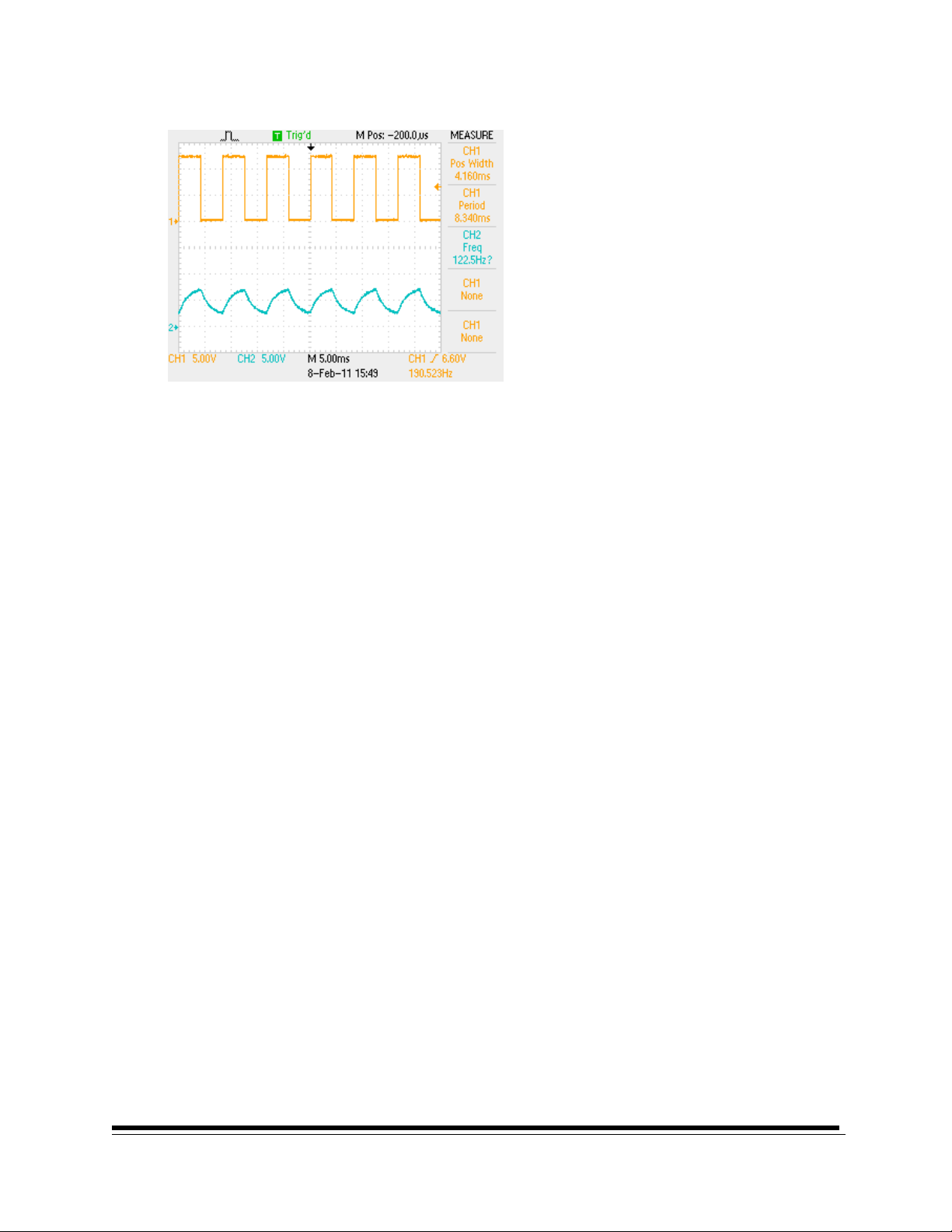
12.8. Observe the voltage at TP7 to verify that the PLL is in lock. The TP7 voltage should be
(+/-.5V) centered at 5 Vdc with a variable amount of ripple dependent on the SIG HI signal. The
TP7 ripple will be at its minimum value at the minimum and maximum SIG HI voltages, as in
Figures 4 and 5, respectively. The TP7 ripple will be at its maximum value when the delay angle
command is near α = 90° as in Figure 6. Sweep the SIG HI voltage over the full range to ensure
that the average voltage does not deviate from 5 Vdc.
Figure 4 VCO control voltage and phase detector waveform, SIG HI = 5.0 Vdc
Channel 1: TP6
Channel 2: TP7
Figure 5 VCO control voltage and phase detector waveform, SIG HI = 0.5 Vdc
Channel 1: TP6
Channel 2: TP7
Enerpro Document No: OP-0106, Rev. B Page 7 of 14 ECO #19-11089; Release Date: 08/02/2019
Figure 6 VCO control voltage and phase detector waveform, SIG HI = 2.75 Vdc
Channel 1: TP6
Channel 2: TP7

Enerpro Document No: OP-0106, Rev. B Page 8 of 14 ECO #19-11089; Release Date: 08/02/2019
13.0 Electrical Specifications
The electrical specifications of the General Purpose Firing Board are summarized in the table
below. Part numbers refer to drawing E168 revision L.
Characteristic Performance Requirement Supporting. Information
1. Board mounted power
supply for control
electronics and SCR
gate drive.
Connect to mains at J3-5 and J3-1 for
240/480V or J3-3 and J3-5 for 120/240V.
24VA 1Ø 50/60Hz fused board mounted
transformer T1. Center-tapped primary
connected for 240V or 480V.
2. SCR gate waveform. Pulse Profile: 180 -
burst with a 32.6µs
pulse width.
3. Input control signal. 0 Vdc to 5.0 Vdc control signal. Input
impedance is 10.0kΩ.
Option : a shunt resistance (R11) across signal
input can be selected for milliamp control
signal.
R11 = 249 Ω for 4 to 20mAdc current control
signal.
4. Gate delay steady-state
transfer function.
Increase in command voltage produces a
proportional decrease in gate delay angle,
.
max. and
min. change equally with change
in Rbias (R6).
( max-min) changes with Rspan (R7).
5. Gate delay dynamic
transfer function
bandwidth.
Attenuation = -3dB at 67Hz. Phase shift =
-45° @ 57Hz.
Frequency response can be modified by
changing summing amplifier parameters.
6. Effect of frequency. ∆/∆f = 1.5°/Hz. For 50Hz operation,
compensate by removing R13.
Jumper J8 for 50/60 selectable operation
7. Lock acquisition time. Approximately 30ms. Gating is inhibited for 20ms or longer at power-
on.
Inhibit period depends on Soft-Start time
constant.
8. Soft-Start Gating commences at
max. and
exponentially decays to the commanded
delay when NOT(I2) is ungrounded (J4-
12).
Soft-Start time constant is set by C2 and R14.
T = (1.5k + R14)(C2)(0.579)
T in ms, R in kΩ, C in µF
R14 ≥ 20.0kΩ
9. Soft-Stop Gate-delay angle ramps to
max. before being inhibited when
NOT(I2) is grounded.
Soft-Stop time constant is set by C2 and R15.
T = R15(C2)(1.84)
R15 ≥ 1.0kΩ
10. Power-on inhibit. Inhibit circuit is activated at power-on. Same delay angle response as with the soft-
start circuit.
11. Low Signal Inhibit Inhibit circuit is activated if SIG HI <
0.5Vdc.
Eliminate this feature by removing CR6.
12. Instantaneous inhibit. Opening the connection of NOT(I1) (P4-4 )
to +12V instantly inhibits SCR gating.
Closing the connection of NOT(I1) to +12V
instantly enables SCR gating.
Gating is inhibited if P4 is removed.
13. Peak gate drive open
circuit voltage
15V With a 30Vdc supply voltage
14. Peak gate drive short
circuit current.
1.7A Measured with a 30 Vdc supply voltage and a
1.0Ω load resistor
15. Gate drive current rise
time(short circuit)
.5A in .5µs Measured with a 30 Vdc supply voltage and a
1.0Ω load resistor
16. Frequency sensitivity 2.6°el./Hz
17. Temp. sensitivity ±2°el. for 0° C<Ta<70° C
18. Ambient temperature. 0°C to 70°C
Enerpro Document No: OP-0106, Rev. B Page 9 of 14 ECO #19-11089; Release Date: 08/02/2019
14.0 TYPICAL CONNECTION DIAGRAMS
Figures 7 through 11 show the basic connections required for several common uses of the
FCRO4100 firing board. If additional information is required, please contact the Enerpro
applications department.
Figure 7. 2-Thyristor In-Line AC Controller
FCRO4100
FIRING BOARD
12
J2
4512
J1 5613
J3
5
+X1 -X1
DELAY
COMMAND
SOFT
INHIBIT
INSTANT
INHIBIT
J4
710 812 11 46
12
on
off
on
off
24
VAC
+5
com
com
+12
I2
I1
gk
Figure 5. 2-Thyristor In-Line AC Controller
-X1
+X1
gk
SINGLE
PHASE
LOAD
Enerpro Document No: OP-0106, Rev. B Page 10 of 14 ECO #19-11089; Release Date: 08/02/2019
FCRO4100
FIRING BOARD
12
J2
4512
J1
5613
J3 5
+X2 -X2 +X1 -X1
DELAY
COMMAND
SOFT
INHIBIT
INSTANT
INHIBIT
J4
710 8 12 11 4 6 12
on
off
on
off
24
VAC
+5
com
com
+12
I2
I1
gk
Figure 7. 4-Thyristor Bridge Rectifier
-X1
+X1
g
k
LOAD
Transformer
+X2
-X2
Figure 8. 4-Thyristor Bridge Rectifier
Figure 9. 2-Thyristor Center Tapped Transformer
Enerpro Document No: OP-0106, Rev. B Page 11 of 14 ECO #19-11089; Release Date: 08/02/2019
FCRO4100
FIRING BOARD
12
J2
4512
J1
5613
J3
5
+X1F -X1F
DELAY
COMMAND
SOFT
INHIBIT
INSTANT
INHIBIT
J4
71081211
4612
on
off
on
off
24
VAC
+5
com
com
+12
I2
I1
gk
Figure 9. 8-Thyristor Two Bridge Rectifiers
+X2F -X2F
POLARITY
COMMAND
reverse
forward
5
P
-X1F
+X1F
g
k
LOAD
+X2F
-X2F -X1R
+X1R
+X2R
-X2R
12
J1
45 12
J2
12
FCOAUX60 AUXILIARY
FIRING BOARD J3
J7
+X2R -X2R
+X1R -X1R
• Cut trace as indicated by note 13 on E168
Figure 10. 8-Thyristor Two Bridge Rectifiers
FCRO4100
FIRING BOARD
12
J2
4512
J1
5613
J3
5
+X1 -X1
DELAY
COMMAND
SOFT
INHIBIT
INSTANT
INHIBIT
J4
710
812 11 4 6 12
on
off
on
off
24
VAC
+5
com
com
+12
I2
I1
gk
Figure 8. 4-Thyristor Center Tapped Transformer
+X2 -X2
POLARITY
COMMAND
reverse
forward
5
P
• Cut trace as indicated by note 13 on E168
-X1
+X1
gk
LOAD
Transformer
+X2
-X2
Figure 11. 4-Thyristor Center Tapped Transformer

Enerpro Document No: OP-0106, Rev. B Page 12 of 14 ECO #19-11089; Release Date: 08/02/2019
15.0 General Specifications
Table 1. Specifications.
Maximum Ratings
AC mains voltage 480 Vac
Pulse transformer hipot 3500 Vac (60 seconds)
Operating temperature range -5 to 85 C
Board ac supply voltage 28 Vac (24 Vac nominal)
12 V regulator output current 20 mA (30 Vdc supply)
5 V reference output current 5 mA (30 Vdc supply)
Auxiliary control power output from 24 Vac/30 Vdc 2 W
Delay angle range 10° ≤ α ≤ 170°
Electrical Characteristics
Delay angle command signal, SIG HI Voltage: 0-5
Current: 4-20 mA
Or per customer specification
Control signal isolation from ground Galvanic isolation provided by pulse
transformers and control power transformers
Gate delay steady-state transfer function Delay angle decreases as SIG HI increases
Gate delay dynamic transfer function bandwidth -3 dB at 67 Hz, phase shift -45° at 57 Hz
Gate drive phase balance ±1° (max)
Delay angle variance Δ(α)/Δ(f) = 1.5°/Hz
50/60 Hz compensation via J3 selection
Lock acquisition time 30 ms (typ)
Soft-start/stop time (independently configurable) 0.05 – 20.0 s (typical)
Low SIG HI inhibit Firing inhibited when SIG HI < 0.48 Vdc.
Remove D6 to defeat this feature
Power-on inhibit Automatic
Instant/soft inhibit/enable inputs Dry contact
Gate pulse burst frequency 256 times line frequency
Initial gate pulse open circuit voltage 15 V (30 Vdc supply)
Sustaining gate pulse open circuit voltage 7.0 V (30 Vdc supply)
Peak gate drive short circuit current 1.5 A (30 Vdc supply, 1.0 Ω gate load)
Sustaining gate drive short circuit current 0.5 A (30 Vdc supply, 1.0 Ω gate load)
Short-circuit gate drive current rise time 1.0 A/μs (30 Vdc supply, 1.0 Ω gate load)
Board dimensions 191 x 152 x 35 mm (L x W x D)
Minimum creepage distance to ac mains 13 mm
Conformal coating per MIL-1-46058, Type UR

Enerpro Document No: OP-0106, Rev. B Page 13 of 14 ECO #19-11089; Release Date: 08/02/2019
Control Signals are supplied
here.
(See Figures 1 and 2.
Also see Dwg. #E168)
CAUTION!
g k g k
CONNECTOR
FOR
T1 EXCITATION
(Board Power)
LOWER VOLTAGE TO
J3 PINS 3 & 5
HIGHER VOLTAGE TO
J3 PINS 1 & 5
N/C
+X2 -X2 +X1 -X1
g k g k
TO SCR'S
J8
J4
6.75"
Center
to Center
5.0"
Center
to Center
WARNING Check these connections very carefully before energizing the firing board. Improper connections
will result in product and/or customer equipment damage! If you have any questions concerning these
connections, call for assistance
J5
J2 J1
COM
"POWER
ON"
Green LED
PD2
"INHIBIT"
RED LED
PD1
J3
120/240
or
240/480
50/60 HZ
PROGRAMMING
Plug for
optional
Regulator
Board
P#
VRCL1P-1
R7
SPAN
R6
BIAS
N/C
N/C
12 3456 135
123 45
2A
2A
J6
PM3 PM4 PM1 PM2
R4
U3
147
AC Current & Voltage
Feedback;
Current Limit Command
FCRO4100

Enerpro Document No: OP-0106, Rev. B Page 14 of 14 ECO #19-11089; Release Date: 08/02/2019
APPENDIX A
The following AMP Mate-N-Lok™ information is provided for your convenience. The part numbers referenced are
valid as of this date and are currently used by Enerpro. However, these numbers are subject to change.
Description
A
MP Numbe
r
Enerpro Stock Numbe
r
J1: 6-position Header (right angle) 640583-1 C2MNLRPH06
J1: 6-position Header (vertical) 350711-1 C2MNLVPH06
P1: 6-position Plug 640581-1 C2MNLPLG06
J2: 5-position Header (right angle) 1-350945-0 C2MNLRPH05
J2: 5-position Header (vertical) 640900-1 C2MNLVPH05
P2: 5-position Plug 350809-1 C2MNLPLG05
J3: 5-position Header (right angle) 1-350945-0 C2MNLRPH05
J3: 5-position Header (vertical) 640900-1 C2MNLVPH05
P3: 5-position Plug 350809-1 C2MNLPLG05
J4: 12-position Header (vertical) 350713-1 C2MNLVPH12
P4: 12-position Plug 350735-1 C2MNLPLG12
J5: 4-position Header (vertical) 350792-1 C2MNLVPH04
P5: 4-position Plug 350779-1 C2MNLPLG04
Contact Socket (20 - 14 AWG) 350552-1 N/A
Keying Plug 1-640415-0 C2KP94V0
Universal Crimp Tool 90287-1 N/A
AMP extraction Tool 458994-2 M2T458994
Table 2. AMP Mate-N-Lok™ Cross Reference
Table of contents
Popular Motherboard manuals by other brands


Gigabyte
Gigabyte GA-G41MT-ES2L user manual

Alpha Microsystems
Alpha Microsystems AM-990 Service manual

Linear Technologie
Linear Technologie DC1619A Demo Manual

mikroElektronika
mikroElektronika mikromedia for PIC24 Schematics

Asus
Asus EX-H310M-X manual

GIGA-BYTE TECHNOLOGY
GIGA-BYTE TECHNOLOGY H510M DS2V user manual


