Fiberplex SFP-BHDVXC-0000-R User manual

USERMANUAL
3GbpsSDISFPCoaxialTransceiver
SFP‐BHDVXC‐0000‐R/SFP‐BHDVXC‐0000‐L

PageIntentionallyLeftBlank

WarningforYourProtection
1.Readtheseinstructions.
2.Keeptheseinstructions.
3.Heedallwarnings.
4.Followallinstructions.
5.Donotusethisapparatusnearwater.
6.Cleanonlywithadrycloth.
7.Donotblockanyoftheventilationopenings.Installinaccordancewiththemanufacturer’sinstructions.
8.Donotinstallnearanyheatsourcessuchasradiators,heatregisters,stoves,orotherapparatus(includingamplifiers)thatproduceheat.
9.Donotdefeatthesafetypurposeofthepolarizedorgrounding‐typeplug.Apolarizedplughastwobladeswithonewiderthantheother.A
groundingtypeplughastwobladesandathirdgroundingprong.Thewidebladeorthethirdprongisprovidedforyoursafety.Iftheprovidedplug
doesnotfitintoyouroutlet,consultanelectricianforreplacementoftheobsoleteoutlet.
10.Protectthepowercordfrombeingwalkedonorpinched,particularlyatplugs,conveniencereceptacles,andthepointwheretheyexitfromthe
apparatus.
11.Onlyuseattachments/accessoriesspecifiedbythemanufacturer.
12.Useonlywiththecart,stand,tripod,bracket,ortablespecifiedbythemanufacturer,orsoldwiththeapparatus.Whenacartisused,use
cautionwhenmovingthecart/apparatuscombinationtoavoidinjuryfromtip‐over.
13.Unplugthisapparatusduringlightningstormsorwhenunusedforlongperiodsoftime.
14.Referallservicingtoqualifiedservicepersonnel.Servicingisrequiredwhentheapparatushasbeendamagedinanyway,suchaspower‐supply
cordorplugisdamaged,liquidhasbeenspilledorobjectshavefallenintotheapparatus,theapparatushasbeenexposedtorainormoisture,does
notoperatenormally,orhasbeendropped.
Theapparatusshallnotbeexposedtodrippingorsplashing.Noobjectsfilledwithliquids,suchasvases,shallbeplacedontheapparatus.
“WARNING:Toreducetheriskoffireorelectricshock,donotexposethisapparatustorainormoisture.”
GeneralInstallationInstructions
Pleaseconsiderthesegeneralinstructionsinadditiontoanyproduct‐specificinstructionsinthe“Installation”chapterofthismanual.
Unpacking
Checktheequipmentforanytransportdamage.Iftheunitismechanicallydamaged,ifliquidshavebeenspilledorifobjectshavefallenintothe
unit,itmustnotbeconnectedtotheACpoweroutlet,oritmustbeimmediatelydisconnectedbyunpluggingthepowercable.Repairmustonlybe
performedbytrainedpersonnelinaccordancewiththeapplicableregulations.
InstallationSite
Installtheunitinaplacewherethefollowingconditionsaremet:
Thetemperatureandtherelativehumidityoftheoperatingenvironmentmustbewithinthespecifiedlimitsduringoperationofthe
unit.Valuesspecifiedareapplicabletotheairinletsoftheunit.
Condensationmaynotbepresentduringoperation.Iftheunitisinstalledinalocationsubjecttolargevariationsofambient
temperature(e.g.inanOB‐van),appropriateprecautionsmustbetaken.
Unobstructedairflowisessentialforproperoperation.Ventilationopeningsoftheunitareafunctionalpartofthedesignandmust
notbeobstructedinanywayduringoperation(e.g.‐byobjectsplaceduponthem,placementoftheunitonasoftsurface,or
improperinstallationoftheunitwithinarackorpieceoffurniture).
Theunitmustnotbeundulyexposedtoexternalheatsources(directsunlight,spotlights).
AmbientTemperature
UnitsandsystemsbyFiberPlexaregenerallydesignedforanambienttemperaturerange(i.e.temperatureoftheincomingair)of5°Cto40°C(41
°Fto104°F).Whenrackmountingtheunits,thefollowingfactsmustbeconsidered:
Thepermissibleambienttemperaturerangeforoperationofthesemiconductorcomponentsis0°Cto+70°C(32°Fto158°F)
(commercialtemperaturerangeforoperation).
Theairflowthroughtheinstallationmustallowexhaustairtoremaincoolerthan70°C(158°F)atalltimes.
Averagetemperatureincreaseofthecoolingairshallbeabout20°C(68°F),allowingforanadditionalmaximum10°Cincreaseat
thehottestcomponents.
Ifthecoolingfunctionoftheinstallationmustbemonitored(e.g.forfanfailureorilluminationwithspotlamps),theexhaustairtemperaturemust
bemeasureddirectlyabovethemodulesatseveralplaceswithintheenclosure.
GroundingandPowerSupply
Groundingofunitswithmainssupply(ClassIequipment)isperformedviatheprotectiveearth(PE)conductorintegratedinthree‐pinPhoenix™
connector.Unitswithbatteryoperation(<60V,ClassIIIequipment)mustbeearthedseparately.Groundingtheunitisoneofthemeasuresfor
protectionagainstelectricalshockhazard(dangerousbodycurrents).Hazardousvoltagemaynotonlybecausedbydefectivepowersupply
insulation,butmayalsobeintroducedbytheconnectedaudioorcontrolcables.
Thisequipmentmayrequiretheuseofadifferentlinecord,attachmentplug,orboth,dependingontheavailablepowersourceatinstallation.If
theattachmentplugneedstobechanged,referservicingtoqualifiedpersonnel.

Warranty,ServiceandTermsandConditionsofSale
ForinformationaboutWarrantyorServiceinformation,pleaseseeourpublished‘TermsandConditionsof
Sale’.Thisdocumentisavailableonfiberplex.comorcanbeobtainedbyrequestingitfrom
[email protected]orcalling301.604.0100.
Disposal
DisposalofPackingMaterials
Thepackingmaterialshavebeenselectedwithenvironmentalanddisposalissuesinmind.Allpackingmaterial
canberecycled.Recyclingpackingsavesrawmaterialsandreducesthevolumeofwaste.Ifyouneedto
disposeofthetransportpackingmaterials,recyclingisencouraged.
DisposalofUsedEquipment
Usedequipmentcontainsvaluablerawmaterialsaswellassubstancesthatmustbedisposedof
professionally.Pleasedisposeofusedequipmentviaanauthorizedspecialistdealerorviathepublicwaste
disposalsystem,ensuringanymaterialthatcanberecycledhasbeen.Pleasetakecarethatyourused
equipmentcannotbeabused.Afterhavingdisconnectedyourusedequipmentfromthemainssupply,make
surethatthemainsconnectorandthemainscablearemadeuseless.
Disclaimer
Theinformationinthisdocumenthasbeencarefullycheckedandisbelievedtobeaccurateatthetimeof
publication.However,noliabilityisassumedbyFiberPlexforinaccuracies,errors,oromissions,norforlossor
damageresultingeitherdirectlyorindirectlyfromuseoftheinformationcontainedherein.
Notice
ThefirmwareincludedinthisproductutilizestheAtmelSoftwareFramework(ASF),Copyright(c)2011‐2012AtmelCorporation.Allrights
reserved.
Redistributionanduseinsourceandbinaryforms,withorwithoutmodification,arepermittedprovidedthatthefollowingconditionsaremet:
1.Redistributionsofsourcecodemustretaintheabovecopyrightnotice,thislistofconditionsandthefollowingdisclaimer.
2.Redistributionsinbinaryformmustreproducetheabovecopyrightnotice,thislistofconditionsandthefollowingdisclaimerinthe
documentationand/orothermaterialsprovidedwiththedistribution.
3.ThenameofAtmelmaynotbeusedtoendorseorpromoteproductsderivedfromthissoftwarewithoutspecificpriorwrittenpermission.
4.ThissoftwaremayonlyberedistributedandusedinconnectionwithanAtmelmicro‐controllerproduct.
THISSOFTWAREISPROVIDEDBYATMEL“ASIS”ANDANYEXPRESSORIMPLIEDWARRANTIES,INCLUDING,BUTNOTLIMITEDTO,THEIMPLIED
WARRANTIESOFMERCHANTABILITY,FITNESSFORAPARTICULARPURPOSEANDNON‐INFRINGEMENTAREEXPRESSLYANDSPECIFICALLY
DISCLAIMED.INNOEVENTSHALLATMELBELIABLEFORANYDIRECT,INDIRECT,INCIDENTAL,SPECIAL,EXEMPLARY,ORCONSEQUENTIALDAMAGES
(INCLUDING,BUTNOTLIMITEDTO,PROCUREMENTOFSUBSTITUTEGOODSORSERVICES;LOSSOFUSE,DATA,ORPROFITS;ORBUSINESS
INTERRUPTION)HOWEVERCAUSEDANDONANYTHEORYOFLIABILITY,WHETHERINCONTRACT,STRICTLIABILITY,ORTORT(INCLUDING
NEGLIGENCEOROTHERWISE)ARISINGINANYWAYOUTOFTHEUSEOFTHISSOFTWARE,EVENIFADVISEDOFTHEPOSSIBILITYOFSUCHDAMAGE.

Introduction
TheSFP‐BHDVXC‐0000‐LisanelectricalSFPTransceivermodulewithoptionalreclockers(SFP‐BHDVXC‐0000‐R)
designedtotransmitandreceiveSDIsignalsupto2.97Gbpsover75ΩcoaxialcablesviaHD‐BNCconnectors.
CabledriverslewrateisautomaticallyconfiguredinordertoachievecompliancetoSMPTE424M/SMPTE
292MandSMPTE259M.EqualizerfeaturesDCrestorationtocompensatefortheDCcontentofSMPTE
pathologicaltestpatterns.OntheSFP‐BHDVXC‐0000‐R,thereclockerprocuresoptimalinput&outputjitter
performancebysuppressingaccumulatedjitter.
TheSFP‐BHDVXCprovidesmoduleidentificationinformationanddiagnosticmonitoringthrougha2wireserial
interface.Itisalsohot‐pluggablesolutionforinfieldsystemupgradeandmaintenance. TheSFP‐BHDVXCis
interchangeablewithothersMSApinoutopticalvideoSFPimprovingproductflexibility.ThemoduleisSMPTE
compliantresultinginquicktime‐to‐marketandreduceddevelopmenteffortandcost.TheSFP‐BHDVXCisPb‐
freeandRoHScompliant.
KeyFeatures
SMPTE424M,SMPTE292M,andSMPTE259Mcompliant
HD‐BNC75Ωconnectors
EqualizesBelden1694Acableupto:140mat2.97Gb/s,200mat1.485Gb/sand400mat270Mb/s
IntegratedReclockerandCableDriver
SupportsDVB‐ASIat270Mb/s
SupportsvideopathologicalpatternsforSD‐SDI,HD‐SDIand3G‐SDI
Hot‐pluggable
Controlviaserialinterfaceincluding:
o Outputslewrate(SDorHD/3G)
o Inputsignaldetection(RX_LOS)
o Voltage&TemperatureMonitoring
o ModuleInformation
o ReclockerRate&LockMonitoring
o BypassReclockerstage
o AutosleepfeatureonRxchannel
LowPowerConsumption‐typical1216mW
SingleSupply+3.3V
Pb‐freeandRoHScompliant
Operatingtemperaturerange:‐40°Cto80°C
58.5mmx13.4mmx8.6mmSFPPackage
GangedCages&StackedCagesmountingsupported
TheoryofOperation
TheSFP‐BHDVXCTransceiverisaSmallFormFactorPluggable(SFP)modulewithcoaxialinterface.HD‐BNC
connectorsareusedtointerfacethemodulewith75Ωcoaxialcables.
TheSFP‐BHDVXCTransceiverwilldrivethedifferentialTD±inputstoitsTXcoaxialoutputifTX_DISinputislow
andSoftTx_Disableislow(Status/Controlregisterbit6).
TheslewrateoftheSFP‐BHDVXC‐0000‐LoutputisconfigurablethroughtheSERIALCONFIGINTERFACEvia
SoftRate_Selectandshallbeconfiguredbasedonthetransmittedsignalstandardtoensurecompliancywith
SMPTEspecification.Atpowerup,thedefaultconfiguredslewrateiscompliantwithHD/3G‐SDIsignal.
BecausethedefaultslewrateisforHD‐SDI&3G‐SDI,thehostshoulddetectifthemodulegetsswappedvia
MOD_DEF0.IfmoduleisreplacedorhotswappedwhiledrivinganSD‐SDIsignal,thenewmodulewillhavethe
wrongslewrateanditwillrequirereconfiguration.TheslewrateoftheSDIoutputsoftheSFP‐BHDVXC‐0000‐
RisautomaticallyconfiguredbythereclockerandiscompliantwithSMPTEspecification.
TheSFP‐BHDVXCTransceiverautomaticallyequalizedthereceivedsignal(RX)forthecablelossandretimes
(reclockerversiononly)serialdigitalvideodataconformingtotheSMPTE424M,292Mand259M.Withouta
validsignaldetected,theLOSoutputisactive(open‐drain).
TheSFP‐BHDVXCTransceivermodulehasaserialinterfacethroughwhichanEEPROMcontainingtheSERIAL
IDENTIFICATIONcanberead.Throughthesameserialinterface,diagnosticmonitoringisprovidedviathe
SERIALCONFIGINTERFACEgivingtheopportunitytoreadthetemperature,thesupplyvoltage,theLOSstatus
andallreclockerfeatures.

GettingStarted
InitialInspection
Immediatelyuponreceipt,inspecttheshippingcontainerfordamage.Thecontainershouldberetaineduntil
theshipmenthasbeencheckedforcompletenessandtheequipmenthasbeencheckedmechanicallyand
electrically.Iftheshipmentisincomplete,ifthereismechanicaldamage,oriftheunitfailstooperatenotify
FiberPlexandmaketheshippingmaterialsavailableforthecarrier'sinspection.
Figure1:HighLevelBlockDiagram‐SFP‐BHDVXC‐0000‐L(standard)
Figure2:HighLevelBlockDiagram‐SFP‐BHDVXC‐0000‐R(withreclocker)
SDI TX Cable Driver
SDI RX EQ
VCC TD+
µC / EEPROM
2
2
2
TD-
TX_DIS
MOD_DEF[1]
MOD_DEF[2]
MOD_DEF[0]
RD+
RD-
VEE
LOS
SDI TX Cable
Driver
SDI RX EQ
VCC TD+
Reclocker
Reclocker
µC / EEPROM
2
2
2
2
2
TD-
TX_DIS
MOD_DEF[1]
MOD_DEF[2]
MOD_DEF[0]
RD+
RD-
VEE
LOS
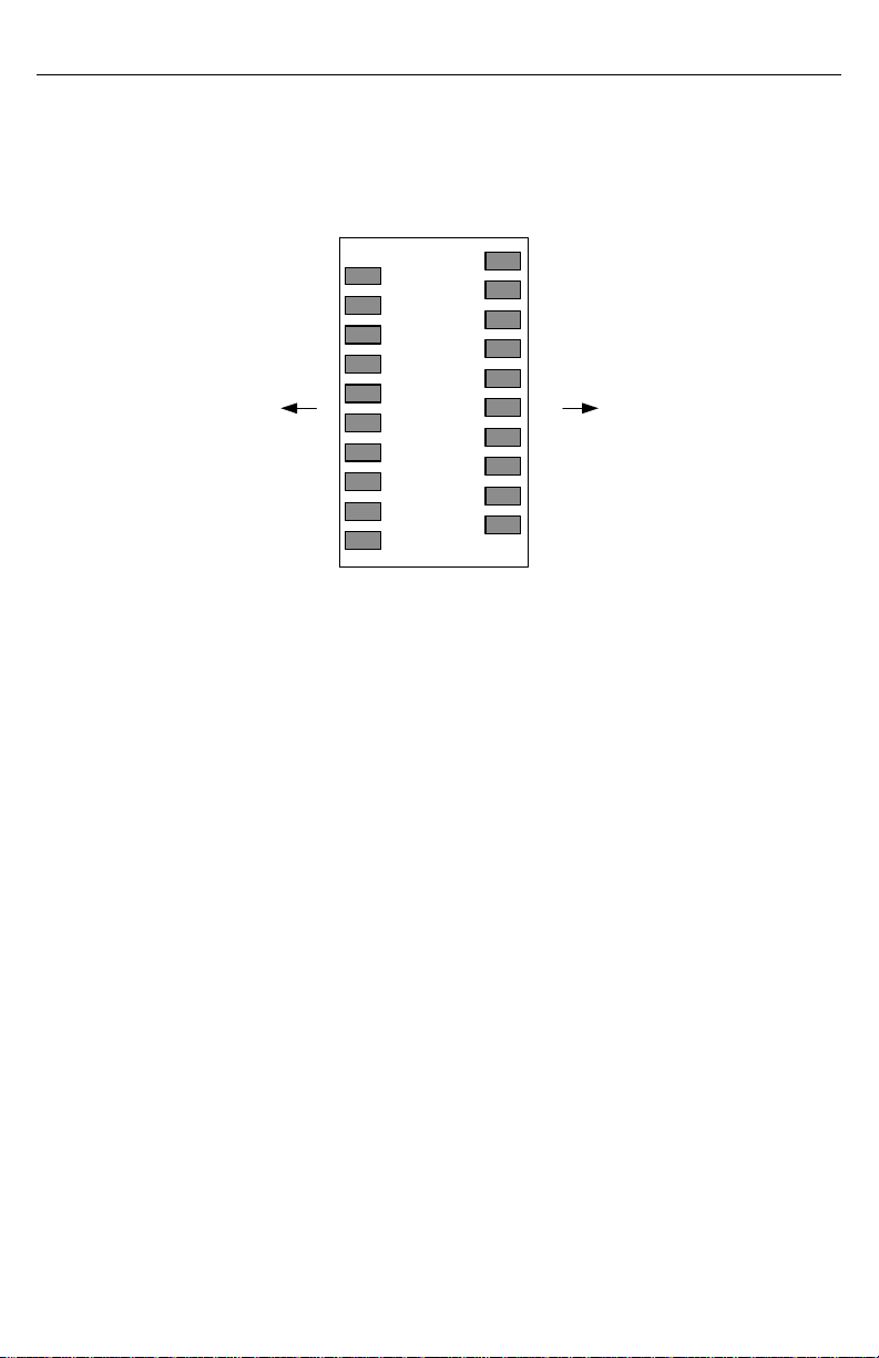
HostConnectorPinConfiguration
Figurebelowshowsthepinnamesandnumberingfortheconnectorblockonthehostboard.Thediagramis
inthesamerelativeorientationasthehostboardlayout.ThepinfunctionsaredescribedinTable1with
accompanyingnotes.TominimizedEMIemission,thesignalstothe20‐pinconnectorshouldbeshutoffwhen
themoduleisremoved.
1
2
3
4
5
6
7
8
9
10
20
VEE
VEE
19
TD-
VEE
18
TD+
TX_DIS
17
VEE
MOD_DEF[2]
16
VCC
MOD_DEF[1]
15
VCC
MOD_DEF[0]
14
VEE
NC (RATE)
13
RD+
LOS
12
RD-
VEE
11
VEE
VEE
Towards
Bezel
Towards
ASIC
Figure3:HostConnectorPinConfiguration

SFPElectricalPadLayout
TheSFPTransceivercontainsaprintedcircuitboardthatmateswiththeSFPelectricalhostconnector.The
padsaredesignedforasequencedmating:
Firstmate–groundcontacts
Secondmate–powercontacts
Thirdmate–signalcontacts
ThedesignofthematingportionoftheSFPTransceiverprintedcircuitboardisillustratedinFigure4.
1
2
3
4
5
6
7
8
9
10
VEE
VEE
TX_DIS
MOD_DEF[2]
MOD_DEF[1]
MOD_DEF[0]
NC (RATE)
LOS
VEE
20 VEE
19 TD-
18 TD+
17 VEE
16 VCC
15 VCC
14 VEE
13 RD+
12 RD-
11 VEE
Top of Board
VEE
Bottom of Board
(As viewed thru top of board)
Bottom of Board
(As viewed thru top of board)
PIN 20
PIN 1
SFP Rear View
Figure4:SFPElectricalPadLayout

Table1:SFPPinDescription
Pin Name Function Notes
1 VEE Ground
2 VEE Ground TX_FAULTneverassertedbythismodule
3 TX_DIS TransmitterDisable TX_DISisanactivehighinputthatisusedtoshutdownthetransmitterelectricaloutput.
Itisinternallypulledupwitha4.7kΩto10kΩresistor.(Theoutputmaybedisabledby
registryevenifTX_DIS=’0’)
High/Open=TransmitterDisabled
Low=TransmitterEnabled
4 MOD_DEF[2] ModuleDefinition2 DefinedasSerialData(SDA).MustbepulleduptoVCC(4.7k‐10kΩ)onthe
hostboard(opendrain).
5 MOD_DEF[1] ModuleDefinition1 DefinedasSerialClock(SCL).MustbepulleduptoVCC(4.7k‐10kΩ)onthe
hostboard(opendrain).
6 MOD_DEF[0] ModuleDefinition0 Groundedbythemoduletoindicatethatthemoduleispresent.
7 NC(RATE) NotConnected Floating;notinternallyconnected
8 LOS Lossofsignal LOSisanactivehighopen‐drainoutputthatreturnsthelossofavalidSDIinputbythe
receiverequalizer.
High=Nocarrierdetected
Low=Carrierdetected
9 VEE Ground
10 VEE Ground
11 VEE Ground
12 RD‐ Inv.ReceivedDataOut RD±arethedifferentialreceiveroutputs.TheyareACcoupled100Ωdifferentiallines
whichshouldbeterminatedwith100ΩdifferentialattheuserSERDES/ASIC.Thevoltage
swingontheselineswillbebetween620mVand880mVdifferentialwhenproperly
terminated.
13 RD+ ReceivedDataOut
14 VEE Ground
15 VCC +3.3VSupply Definedas3.3V±5%atetheSFPconnectorpin.Recommendedhostboardpowerfiltering
isshowninfigure5.2.Whentherecommendedsupplyfilteringnetworkisused,hot
pluggingofmodulewillresultinaninrushcurrentofnomorethan30mAgreaterthan
thesteadystatevalue.
16 VCC +3.3VSupply
17 VEE Ground
18 TD+ TransmitDataIn TD±arethedifferentialinputsofthetransmitter.TheyareACcoupleddifferentiallines
with100Ωdifferentialterminationinsidethemodule.TheACcouplingisdoneinsidethe
moduleandisthusnotrequiredonthehostboard.Theinputswillacceptdifferential
swingof200mVto1600mV.
19 TD‐ Inv.TransmitDataIn
20 VEE Ground
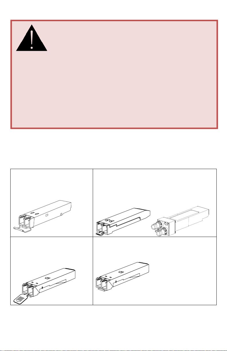
GeneralInstructionsforInsertingandRemovingSFPModules
IdentifytheLatchTypeoftheSFPModule
SFPModuleshavevariouslatchingmechanismstosecurethemintotheSFPCageofadevice.TheFiberPlex
WDMcansupportahostofmanufacturersandbrandsofSFPModulessotheusermayencounteranynumber
ofdifferentlatches.Someofthesearedescribedbelow.
BailClasp
ThebailclaspSFPmodulehasaclasp
thatyouusetoremoveorinstalltheSFP
module.
ActuatorButton
TheactuatorbuttonSFPmoduleincludesabuttonthatyou
pushinordertoremovetheSFPmodulefromaport.This
buttoncaneitherlift‘Up’orpress‘In’toreleasetheSFP
Moduledependingonthemanufacturer.
MylarTab
TheMylartabSFPmodulehasatabthat
youpulltoremovethemodulefroma
port.
SlideTab
TheslidetabSFPmodulehasatabunderneaththefrontofthe
SFPmodulethatyouusetodisengagethemodulefromaport.
HandlingWarnings
SFPModulesarestaticsensitive.Topreventdamagefromelectrostaticdischarge(ESD),itis
recommendedtoattachanESDpreventativewriststraptoyourwristandtoabaremetalsurfacewhen
youinstallorremoveanSFPModule.
DisconnectallopticalorcoppercablesfromSFPModulespriortoinstallingorremovingtheSFPModule.
Failuretodosocouldresultindamagetothecable,cableconnectorortheSFPModuleitself.Removing
andinsertinganSFPModulecanshortenitsusefullife,soyoushouldnotremoveandinsertSFPModules
anymoreoftenthanisabsolutelynecessary.
ProtectopticalSFPmodulesbyinsertingcleandustcoversintothemafterthecablesareremoved.Be
suretocleantheopticsurfacesofthefibercablesbeforeyouplugthembackintotheopticalportsof
anotherSFPmodule.AvoidgettingdustandothercontaminantsintotheopticalportsofyourSFP
modules,becausetheopticswillnotworkcorrectlywhenobstructedwithdust.
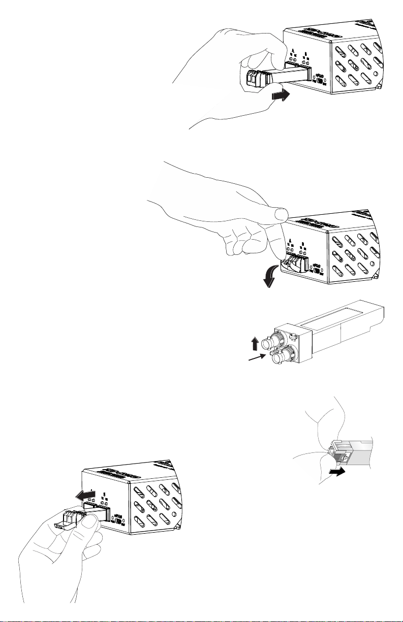
InsertingaModule
1) AttachanESD‐preventative
wristoranklestrap,followingits
instructionsforuse.
2) Disconnectandremoveall
interfacecablesfromSFP
Module.
3) IftheSFPModulehasaBail
Clasp,closetheBailClasp
beforeinsertingtheSFP
Module.
4) Withthegoldfingerconnectoronthebottomandthelabelonthetop,lineuptheSFPModule
withtheemptycageandslideitinmakingsurethatitiscompletelyinsertedandseatedinthe
cage.
RemovingaModule
1) AttachanESD‐
preventativewristor
anklestrap,followingits
instructionsforuse.
2) Disconnectandremoveallinterface
cablesfromSFPModule.
3) Releasethelatchingmechanism.
BailClasp–OpenthebailclaspontheSFP
Modulewithyourfingerinadownward
direction.
ActuatorButton–Gentlypressthe
actuatorup(orin)whilepullingthe
bodyoftheSFPModuletoreleasethe
SFPModulefromthecage.
MylarTab–Pullthetabgentlyina
straightoutwardmotionuntilit
disengagesfromtheport.Makesure
thetabisnottwistedwhenpullingasitmaybecomedisconnectedfromtheSFP
Module.
SlideTab‐Withyourthumb,pushtheslidetabonthe
bottomfrontoftheSFPmoduleinthedirectionofthe
equipmenttodisengagethemodulefromthelinecard
port.IfyoupullontheSFPmodulewithoutdisengaging
thetab,youcandamagetheSFPmodule.
4) GrasptheSFPModulebetweenyourthumbandindex
fingerandcarefullyremoveitfromtheport
5) PlacetheSFPModuleonanantistaticmat,or
immediatelyplaceitinastaticshieldingbagorcontainer
A
ctuator Button

SerialIdentification(EEPROM)
TheSFP2‐wireserialinterface(MOD_DEF1/MOD_DEF2)providesaccesstothe
identificationinformationdescribingSFPcapabilities,interfaces,andassociated
information.Theserialinterfaceusesthe2‐wireserialEEPROMprotocoldefined
fortheATMELAT24C02familycomponent.Thememoryisorganizedasaseries
of8‐bitdatawordsthatcanbeaddressedindividuallyorsequentially.The
contentoftheSERIALIDENTIFICATION(serialID)deviceiswrite‐protected.The
2‐wireserialbusaddress1010000X(A0h)isusedforserialIDaccess.
Thetablebelowdefinestheinformationstructuresthatareobtainedfromthe
SFPTransceiverviatheserialID.
Table2:SerialIdentificationRegisters
Addr RegistryName RegistryDescription Value
BASEIDFIELDS
0 Identifier Typeofserialtransceiver
Vendorspecific–VideotransceiverMSA
80h
1 Ext.Identifier Extendedtypeofserialtransceiver
SFPfunctionisdefinedbyserialIDonly
04h
2 Connector Connectortype
Vendorspecific‐HD‐BNC
82h
3 Transceiver Electronicoropticalcompatibility
SMPTE259M,344M,292M,424M
82h
4
Reserved
MSAdonotspecifyanySMPTEstandardcode 00h
5 00h
6 00h
7 00h
8 00h
9 00h
10 00h
11 Encoding
Codeforserialencodingalgorithm
Unallocated‐NRZI
07h
12 BR,Nominal Nominalbitrate,unitsof100Mbps
3Gbps
1Eh
13 Reserved
Reserved
00h
14
Reserved
Reserved
FiberNotSupported
00h
15 00h
16 00h
17 00h
18 Length(Copper) Lengthsupported(cooper)inm
255m(Varywithbitrate)
FFh
19 Reserved Reserved 00h
20 Vendorname SFPtransceivervendorname(ASCII)
“FIBERPLEX”
46h
21 49h
22 42h
23 45h
24 52h
25 50h
26 4Ch
27 45h
28 58h
29 20h
30 20h
31 20h
32 20h
33 20h
0
95
127
Serial ID defined by
SFP MSA
(96 bytes)
Two wire Address A0h (10100000Xb)
Vendor specific
(32 bytes)
Figure5 EEPROMmemorymapping

Addr RegistryName RegistryDescription Value
34 20h
35 20h
36 Reserved Reserved 00h
37 VendorOUI SFPvendorIEEEcompanyID 00h
38 00h
39 00h
40 VendorPN Partnumber(ASCII)
“SFP‐BHDVXC”
53h
41 46h
42 50h
43 2Dh
44 42h
45 48h
46 44h
47 56h
48 58h
49 43h
50 20h
51 20h
52 20h
53 20h
54 20h
55 20h
56‐59 Vendorrev Revisionlevelforpartnumber(ASCII) XXh…
60‐62 Reserved
Reserved
00h
63 CC_BASE checksum(8lsbresult)(add.0‐62)
XXh
EXTENDEDIDFIELDS
64
Options
optionalSFPsignalsareimplemented
Tx_Disableimplemented
LOSimplemented
00h
65 12h
66 BR,max Upperbitratemargin,unitof%
00h
67 BR,min Lowerbitratemargin,unitof%
00h
68‐83 VendorSN Serialnumber(ASCII)
XXh…
84‐91 Datecode Vendor'smanufacturingdatecode
XXh…
92 Diagnostic
Monitoring
DiagnosticMonitoring
DigitalDiagnosticmonitoringimplementedInternallycalibrated
60h
93 EnhancedOptions EnhancedOptions
SoftTx_DIsablecontrol
SoftRX_LOSmonitoring
50h
94 SFF‐8472
Compliance
SFF‐8472Compliance
Digitaldiagnosticfunctionalityundefined
00h
95 CC_EXT Checksum(add.64‐94)
XXh
VENDORSPECIFICIDFIELDS
96† VendorSpecific AdvancedEnhancedOptions
EQAutosleepControl
01h
96‡ VendorSpecific AdvancedEnhancedOptions1(TXChannel)
Bit3:ReclockerRateMonitoring
Bit2:ReclockerBypassControl
Bit1:ReclockerLockMonitoring
0Eh
97‡ VendorSpecific AdvancedEnhancedOptions2(RXChannel)
Bit2:ReclockerBypassControl
Bit1:ReclockerLockMonitoring
Bit0:EQAutosleepControl
07h
98‐127 VendorSpecific VendorSpecific XXh…
Notes:
1. ThevalueswithXXharedeterminedduringmanufacturing
2. Addresses68‐83specifytheVendorSerialNumber
3. Addresses84‐91specifytheManufacturingDateCode(YYMMDD:YY=Year,MM=Month,DD=Day)
4. Address63containsthechecksumforbyte0‐62
5. Address95containsthechecksumforbyte64‐94
†:StandardOnly‡:ReclcockerOnly

SerialConfigurationInterface
TheSFP2‐wireserialinterface(MOD_DEF1/MOD_DEF2)providesalsodigitaldiagnosticmonitoringviathe
SERIALCONFIGINTERFACE.Theserialinterfaceusesthe2‐wireserialEEPROMprotocoldefinedfortheATMEL
AT24C02familycomponent.Thememoryisorganizedasaseriesof8‐bitdatawordsthatcanbeaddressed
individuallyorsequentially.The2‐wireserialbusaddress1010001X(A2h)isusedforSERIALCONFIG
INTERFACEaccess.
Figure6SerialConfigInterfaceMemoryMapping
ThetablebelowdefinestheinformationstructuresthatareobtainedfromtheSFPTransceiverviatheSERIAL
CONFIGINTERFACE.
Table3:SerialConfigurationInterfaceRegisters
Addr FieldName RegistryName Description Default
Value
(hex)
Default
Value
(dec)
0
Alarm&
Warning
Thresholds
TempHighAlarm(MSB) InternalTemperatureHighAlarmThreshold 55h +85°C
1 TempHighAlarm(LSB) 00h
2 TempLowAlarm(MSB) InternalTemperatureLowAlarmThreshold D8h ‐40°C
3 TempLowAlarm(LSB) 00h
4 TempHighWarning(MSB) InternalTemperatureHighWarningThreshold 50h +80°C
5 TempHighWarning(LSB) 00h
6 TempLowWarning(MSB) InternalTemperatureLowWarningThreshold DDh ‐35°C
7 TempLowWarning(LSB) 00h
8 VoltageHighAlarm(MSB) InternalVoltageHighAlarmThreshold 8Ch +3.6V
9 VoltageHighAlarm(LSB) A0h
10 VoltageLowAlarm(MSB) InternalVoltageLowAlarmThreshold 75h +3.0V
11 VoltageLowAlarm(LSB) 30h
12 VoltageHighWarning(MSB) InternalVoltageHighWarningThreshold 87h +3.47V
13 VoltageHighWarning(LSB) 8Ch
14 VoltageLowWarning(MSB) InternalVoltageLowWarningThreshold 7Ah +3.14V
15 VoltageLowWarning(LSB) A8h
16‐39 NA . NotApplicable XXh..
40‐55 Unallocated Unallocated Reserved XXh...
56‐91 ExtCal
Constant
NA NotApplicable XXh..
92‐94 Unallocated Unallocated Reserved XXh...
95 CC_DMI Checksum Checksum XXh
96
Diagnostics
Temperature(MSB) MeasuredInternalTemperature XXh °C
97 Temperature(LSB) XXh
0
95
55
119
127
Alarm and Warning
Thresholds
(56 bytes)
Cal Constants
(40 bytes)
Vendor Specific
(8bytes)
Two wire Address A2h (10100001Xb)
Real Time Diagnosc
Interface
(24 bytes)

Addr FieldName RegistryName Description Default
Value
(hex)
Default
Value
(dec)
98 Vcc(MSB) MeasuredInternalVoltage XXh V
99 Vcc(LSB) XXh
100‐105 NA NotApplicable XXh...
106‐109 Unallocated Unallocated Reserved XXh...
110 Status/Control Status/Control Seebelowforbitdefinition XXh
MSBLSB
b7 b6 b5 b4 b3 b2 b1 b0
r r/w r r r r r r
TX_DISState
TX_DISinputpin
statecanberead
viathisbit
Soft
Tx_Disable
Select
1=ForceDisableTX
0=UseTX_DISpin
(default)
NA NA Soft
Rate_Select
1=HD/3GSlewRate
(default)
0=SDSlewRate
NA LOS
1=NoInputDetect
0=InputDetect
Data_Ready
State
1=Powerup
0=Dataready
‘X’ ‘0’ ‘0’ ‘0’ ‘0’ ‘0’ ‘X’ ‘X’
111 Reserved Reserved Reserved XXh
112 AlarmFlags AlarmFlags Seebelowforbitdefinition XXh
MSBLSB
b7 b6 b5 b4 b3 b2 b1 b0
r r/w r r r r r r
TempHigh
Alarm
1=AlarmActive
0=AlarmInactive
TempLow
Alarm
1=AlarmActive
0=AlarmInactive
VccHigh
Alarm
1=AlarmActive
0=AlarmInactive
VccLow
Alarm
1=AlarmActive
0=AlarmInactive
NA NA NA NA
‘X’‘X’‘X’‘X’‘0’‘0’‘0’‘0’
114‐115 Unallocated Unallocated Reserved XXh...
116 WarningFlags WarningFlags Seebelowforbitdefinition XXh
MSB LSB
b7 b6 b5 b4 b3 b2 b1 b0
r r/w r r r r r r
TempHigh
Warning
1=WarningActive
0=WarningInactive
TempLow
Warning
1=WarningActive
0=WarningInactive
VccHigh
Warning
1=WarningActive
0=AlarmInactive
VccLow
Warning
1=WarningActive
0= WarningInactive
NA NA NA NA
‘X’‘X’‘X’‘X’‘0’‘0’‘0’‘0’
117 NotApplicable NotApplicable XXh
118 Ext ExtStatus/Control NotApplicable XXh
119 Status/Control Unallocated Reserved XXh
120 VendorSpecific AdvancedStatus/Control1TX
Channel
Seebelowforbitdefinition XXh
MSB LSB
b7 b6 b5 b4 b3 b2 b1 b0
r r/w r r r r r r
NA NA NA NA Reclocker
Rate‡
1=HD/3G
0=SD
Reclocker
Bypass‡
1=Bypass
0=Auto‐Bypass
(default)
Reclocker
Lock‡
1=LockDetect
0=NotLock
Autosleep3
1=EnableAutosleep
(default)
0=DisableAutosleep
‘0’‘0’‘0’‘0’‘X’‘0’‘X’‘1’

Addr FieldName RegistryName Description Default
Value
(hex)
Default
Value
(dec)
ReclockerRate:IndicateswhetherthereclockerisprocessingSDorHD/3Gdatarates.
ReclockerBypass:WhentheBypassbitsetto‘1’,itforcesthedevicetooutputthedatawithoutreclockingit.IftheBypassbitisset
to‘0’,thedeviceautomaticallybypassesthereclockingfunctionwhenthedeviceisanunlockedconditionorthedetectedrateisa
ratewhichthedevicedoesnotsupport.NotethatwhentheBypassinputissetto‘1’,Lockdetectwillremainlow.
ReclockerLock:WhentheLockbitegal‘1’,itindicatesthatdataisbeingreceivedandthePLLislocked.NotethatwhentheBypass
bitissetto‘1’,Lockdetectwillremain‘0’.
121‐123 VendorSpecific VendorSpecific Reserved XXh...
124‡ VendorSpecific AdvancedStatus/Control2
RXChannel
Seebelowforbitdefinition XXh
MSB LSB
b7 b6 b5 b4 b3 b2 b1 b0
r r/w r r r r r r
NA NA NA NA NA Reclocker
Bypass
1=Bypass
0=Auto‐Bypass(default)
ReclockerLock
1=LockDetect0=Not
Lock
Autosleep3
1=EnableAutosleep
(default)
0=Disable A utosleep
‘0’‘0’‘0’‘0’‘0’‘0’‘X’‘1’
ReclockerBypass:WhentheBypassbitsetto‘1’,itforcesthedevicetooutputthedatawithoutreclockingit.IftheBypassbitisset
to‘0’,thedeviceautomaticallybypassesthereclockingfunctionwhenthedeviceisanunlockedconditionorthedetectedrateisa
ratewhichthedevicedoesnotsupport.NotethatwhentheBypassinputissetto‘1’,Lockdetectwillremainlow.
ReclockerLock:WhentheLockbitegal‘1’,itindicatesthatdataisbeingreceivedandthePLLislocked.NotethatwhentheBypass
bitissetto‘1’,Lockdetectwillremain‘0’.
Autosleep:IftheAutosleepbitissetto‘1’,theSFPequalizergoesintoapowersavemodewhennosignalisdetected.Theequalizer
poweronagainonceaninputisdetected.TheAutosleepfunctionalitycanbeturnedoffbysettingAutosleepbitto‘0’.
122‐127 VendorSpecific VendorSpecific Reserved XXh…
Notes:
1. ThevalueswithXXhareeitherdeterminedduringmanufacturingordependonSFPstate
2. Address95containsthechecksumforbyte64‐94
3. Autosleepenables\disablestheSaveMode
†:StandardOnly‡:ReclcockerOnly

Measurementsarecalibratedoveroperatingtemperatureandvoltageandshouldbeinterpretedasdefined
below.Alarmandwarningthresholdvaluesshouldbeinterpretedinthesamemannerasrealtime16bitdata.
Internallymeasuredtemperature
Thetemperatureisrepresentedasa16bitsignedtwo’scomplementvalueinincrementsof1/256°C,yielding
atotalrangeof‐128°Cto+128°C.Themeasuredrangeislimitedtotheoperatingrecommendedconditions.
Toconverta16bitdigitalvalueinCelsius,takedirectlythe16‐bitvalueanddivideitby256°C.Iftheresultis
greaterorequalto128,subtract256fromtheresult.
Table4:Temperatureconversionexamples
16‐bitvalue Temperature
MSB LSB
4Bh 00h +75°C
4Bh 80h +75.5°C
DDh 00h ‐35°C
DCh 80h ‐35.5°C
Internallymeasuredsupplyvoltage
Thevoltageisrepresentedasa16bitunsignedintegerwiththevoltagedefinedasthefull16bitvalue(0–
65535)withLSBequalto100μVolt,yieldingatotalrangeof0to+6.55Volts.Themeasuredrangeislimitedto
theoperatingrecommendedconditions.Toconverta16bitdigitalvalueinVolt,takedirectlythe16‐bitvalue
andmultiplyitby100μVolt.
Table5:Voltageconversionexamples
16‐bitvalue SupplyVoltage
MSB LSB
80h E8h +3.3V
7Eh F4h +3.25V
AlarmsandWarnings
AnAlarmoraWarningflagissetifthemeasuredtemperatureorvoltageexceedthecorrespondingAlarmor
Warningthresholdvalue.

OtherConsiderations
VideoOptimization
TheSocietyofMotionPictureandTelevisionEngineers,orSMPTE,isaleaderinthedevelopmentofstandards
forfilm,television,andothervideo.TheSerialDigitalInterfaceorSDI,wasstandardizedbySMPTEfor
broadcastqualitydigitalvideotransmission.Otherstandardsevolvedfromthisoriginalstandard,defining
Enhanced,High‐definition(HD),3G‐SDI(1080p)andUltraHigh‐definition(UHD),or4Kvideo(2160p).
Tohelpensureerror‐freetransmission,thestandardsincludeadatascrambler/descramblertocreateahigh
densityoftransitionsintheserialdata,makingiteasierforthereceivertomaintaintiming.Wherean
encodingmethodsuchas8B‐10Bensuresaminimalsequentialrunofallonesorzeros,itdoessoatthecost
ofa25%increaseinbandwidthrequirements.Thescrambler/descramblermethoddoesnotrequirethis,but
asaresulttherearecertaincombinationsofscramblerstateandthenextdatabitstobescrambledthatresult
inasequenceofuptotwentyconsecutiveonesorzeros.Thesesequencesarereferredtoaspathological
conditions,andarepresentinspecificshadesofpinkorgrey.
ThesepathologicalconditionsmaycreateerrorsintransmissionthroughtypicalACcoupledoptics,orany
otherACcoupledinterface.VideoEnhancedorSMPTECompliantopticsaredesignedtoacceptthese
pathologicalconditions,allowingthelongersequencesofonesorzerostopasswithouterror.
SFPMSACompliance
TheSFPMulti‐SourceAgreement(MSA)isanagreementthatwasdraftedamongcompetingmanufacturersof
SFPopticalmodules.TheSFFCommitteewasformedtooverseethecreationandmaintenanceofthese
agreementsincludingtheSFPMSAdesignatedasINF‐8074i.Thisagreementdescribesamutuallyagreedupon
standardfortheformandfunctionofSFPmodules.However,notallSFPsproducedareMSAcompliant.The
MSAprovidesforatransceiver(TX/RX)pinout.OtherindustriessuchasbroadcasthadtheneedfordualTX
anddualRXSFPforunidirectionalapplicationssuchasvideo.Naturally,anon‐MSAstandardwasintroduced
allocatingpinoutassignmentsfordualoutputanddualinputI/Oconfigurations.Inaddition,thesomeofthe
internalserialcommunicationpinswerereassigned.
Table6:PinoutComparisonChart
PIN Transceiver(MSA) Transceiver(Non‐MSA) DualTX(Non‐MSA) DualRX(Non‐MSA)
1 VEE VEE VEE VEE
2 TX_FAULT[VEE] VEE NC Rx2‐
3 TX_DIS NC NC Rx2+
4 MOD_DEF(2)‐SDA VEE VEE VEE
5 MOD_DEF(1)‐SCL SCL SCL SCL
6 MOD_DEF(0)–PRESENCE[VEE] SDA SDA SDA
7 Rate[NC] VEE VEE VEE
8 LOS RX1_LOS Tx2+ NC
9 VEE NC Tx2‐ NC
10 VEE NC Tx2_DIS NC
11 VEE VEE VEE VEE
12 RD‐ Rx1‐ NC Rx1‐
13 RD+ Rx1+ NC Rx1+
14 VEE VEE VEE VEE
15 VCC VCC VCC VCC
16 VCC VCC VCC VCC
17 VEE VEE VEE VEE
18 TD+ Tx1+ Tx1+ NC
19 TD‐ Tx1‐ Tx1‐ NC
20 VEE Tx1_DIS Tx1_DIS NC

RecommendedCircuitSchematic
HostBoardRecommendedCircuitSchematic
Next figure shows an example of a complete SFP host board schematic with connections to
SerDes/ASIC and protocolICs.
Figure7:HostCircuit
HostBoardRecommendedPowerSupply
Figure8showstherecommendedpowersupplyfilteringnetwork.
Figure8:HostPowerSupply
PCBLayoutRecommendation
StandardboardlayoutpracticessuchasconnectionstoVccandGNDplaneswithvias,useofshortandequal‐
lengthdifferentialsignaltracesarerecommended.
RD±shallberoutedas100Ωdifferentialcontrolledimpedancetraces.
TD±shallberoutedas100Ωdifferentialcontrolledimpedancetraces.
Forcage&hostconnectorlayout,pleaserefertomanufacturerdocumentation.
Cable Driver
EQ
uC / EEPROM
HD-BNC
HD-BNC
TX SDI
RX SDI
SFP MODULE
LOS
RD-
RD+
SCL
SDA
TD-
TD+
TX_DIS
4.7k 4.7k
100
100
4.7k
+3.3V +3.3V
+3.3V
4.7k
+3.3V
ASIC
ASIC
PROTOCOL
IC
MOD_DEF(2)
MOD_DEF(1)
PRESENCE MOD_DEF(0)
4.7k
+3.3V
HOST
SFP Module Host Board
VCC
1 uH
1 uH
0.1uF
0.1uF 0.1uF
10uF
10uF 10uF
VCC 3.3V

Specifications
ELECTRICALSPECIFICATIONS
AbsoluteMaximumRatings Symbol Min Typ Max Unit
Exceedinganyoftheseratingsmaypermanentlydamagethemodule.Exposuretoabsolutemaximumratingconditionsfor
extendedperiodsmayaffectdevicereliability.
AbsoluteMaximum VoltageRange VCC_MAX 0 3.3 3.6 VDC
Environmental
StorageTemperature Ts ‐40 ‐ +85 °C
OperatingTemperature TC_MAX ‐40 ‐ +80 °C
OperatingRelativeHumidity(noncondensing) 5 ‐ 95 %
ESDRating ‐ ‐ 1 kVHBM
RecommendedOperatingConditions Symbol Min Typ Max Unit
Unlessotherwisespecified,allspecificationsarevalidundertheseconditions:VCC=3.3V±5%,TC=‐40°Cto+80°C.
Specificationsareguaranteedbydesignandcharacterization.
Recommended
OperatingConditions
SupplyVoltage VCC 3.13 3.3 3.465 VDC
OperatingCaseTemperature TC ‐40 ‐ +80 °C
SerialDataRateSD(SMPTE259M,C) BRSD ‐ 270 ‐ Mbps
SerialDataRateHD(SMPTE292M) BRHD ‐ 1483,1485 ‐ Mbps
SerialDataRate3GSMPTE(424M) BR3G ‐ 2967,2970 ‐ Mbps
DCcharacteristics
PowerSupplyCurrent1(RX1<140m)I
CC ‐ 348 402 mA
PowerSupplyCurrent1(RX1>140m)I
CC ‐ 368 427 mA
PowerSupplyCurrent2(SaveMode)I
CC(SaveMode) ‐ 288 331 mA
TotalPowerConsumption1(RX1>140m)P
D ‐ 1216 1410 mW
1. Allpowerconsumptioncharacterisedat25°C
2. SaveModeisactivatedwhenAutosleepregisterissetHIGHandnoinputisdetectedonRXChannel
DigitalI/OCharacteristics‐Logic Symbol Min Typ Max Unit
TX_DIS(Input)
InputVoltageLow VIL‐ ‐ 0.8V
InputVoltageHigh VIH2.0 ‐ ‐ V
Rpull‐up RPU 4.7 ‐ 10 kΩ
LOS(Output) OutputVoltageLow(IOL=10μA) VOL‐ ‐ 0.1 V
OutputVoltageLow(IOL=8.5μA) ‐ ‐ 0.6 V
MOD_DEF2(Output) OutputVoltageLow(IOL=10μA) VOL‐ ‐ 0.1 V
OutputVoltageLow(IOL=8.5μA) ‐ ‐ 0.6 V
MOD_DEF1&
MOD_DEF2(Input)1
InputVoltageLow VIL‐ ‐ 0.8V
InputVoltageHigh VIH2.0 ‐ ‐ V
1. MOD_DEF1(SCL)&MOD_DEF2(SDA)mustbepulleduptoVCCwitha4.7k‐10kΩonthehostboard
DigitalI/OCharacteristics‐Data Symbol Min Typ Max Unit
RD±(Output)1
Single‐endedVoltageSwing3V
OP‐P 310 375 440 mVP‐P
DifferentialVoltageSwing3V
ODIFFP‐P 620 750 880 mVP‐P
DifferentialImpedance3Z
ODIFF 90 100 110 Ω
RiseTime,FallTime3(20%‐80%) tr,tf ‐ 90 130 ps
SerialDataOutputJitter4,5,6
tJIT‐SD ‐ 0.01 0.03 UI
tJIT‐HD ‐ 0.03 0.04 UI
tJIT‐3G ‐ 0.06 0.08 UI
ReclockerLoopBandwidth(270Mbps,<0.1dBPeaking)BW
LOOP‐SD ‐ 275 ‐ KHz
(1485 Mbps,<0.1dBPeaking) BWLOOP‐HD‐ 1.5 ‐ MHz
(2970 Mbps,<0.1dBPeaking) BWLOOP‐3G ‐ 2.75 ‐ MHz
ReclockerAcquisitionTime7T
ACQ ‐ ‐ 15 ms
TD±(Input)2
DifferentialVoltageSwing VIDIFF 200 ‐ 1600 mVP‐P
DifferentialImpedance ZIN 90 100 110 Ω
InputRiseTime/FallTime(270Mbps) tr‐,t
f
‐ ‐ ‐ 1500 ps
(1485Mbps) tr,tf ‐ ‐ 270 ps
(2970Mbps) tr,tf ‐ ‐ 135 ps
SerialInputJitterTolerance
(A1‐TimingJitter–RP184‐1996)
(A2‐AlignmentJitter‐RP184‐1996)
TOLJIT‐SD‐A1 >6 ‐ ‐ UIP‐P
TOLJIT‐SD‐A2 >0.6 ‐ ‐ UIP‐P
TOLJIT‐HD‐A1 >6 ‐ ‐ UIP‐P
TOLJIT‐HD‐A2 >0.6 ‐ ‐ UIP‐P
TOLJIT‐3G‐A1 >6 ‐ ‐ UIP‐P
TOLJIT‐3G‐A2 >0.6 ‐ ‐ UIP‐P
ReclockerLoopBandwidth(270Mbps,<0.1dBPeaking)BW
LOOP‐SD ‐ 275 ‐ KHz
(1485 Mbps,<0.1dBPeaking) BWLOOP‐HD‐ 1.5 ‐ MHz
(2970 Mbps,<0.1dBPeaking) BWLOOP‐3G ‐ 2.75 ‐ MHz
ReclockerAcquisitionTime7T
ACQ ‐ ‐ 15 ms
This manual suits for next models
1
Table of contents
Other Fiberplex Transceiver manuals


Popular Transceiver manuals by other brands


Kenwood
Kenwood TM-241A instruction manual

Kenwood
Kenwood TK-373G Service manual

Yaesu
Yaesu FT-2800M Technical supplement

Kenwood
Kenwood TM-211A instruction manual

Williams Sound
Williams Sound Digi-Wave 300 Series user manual

Advanced Wireless Communications
Advanced Wireless Communications awr2108 owner's manual