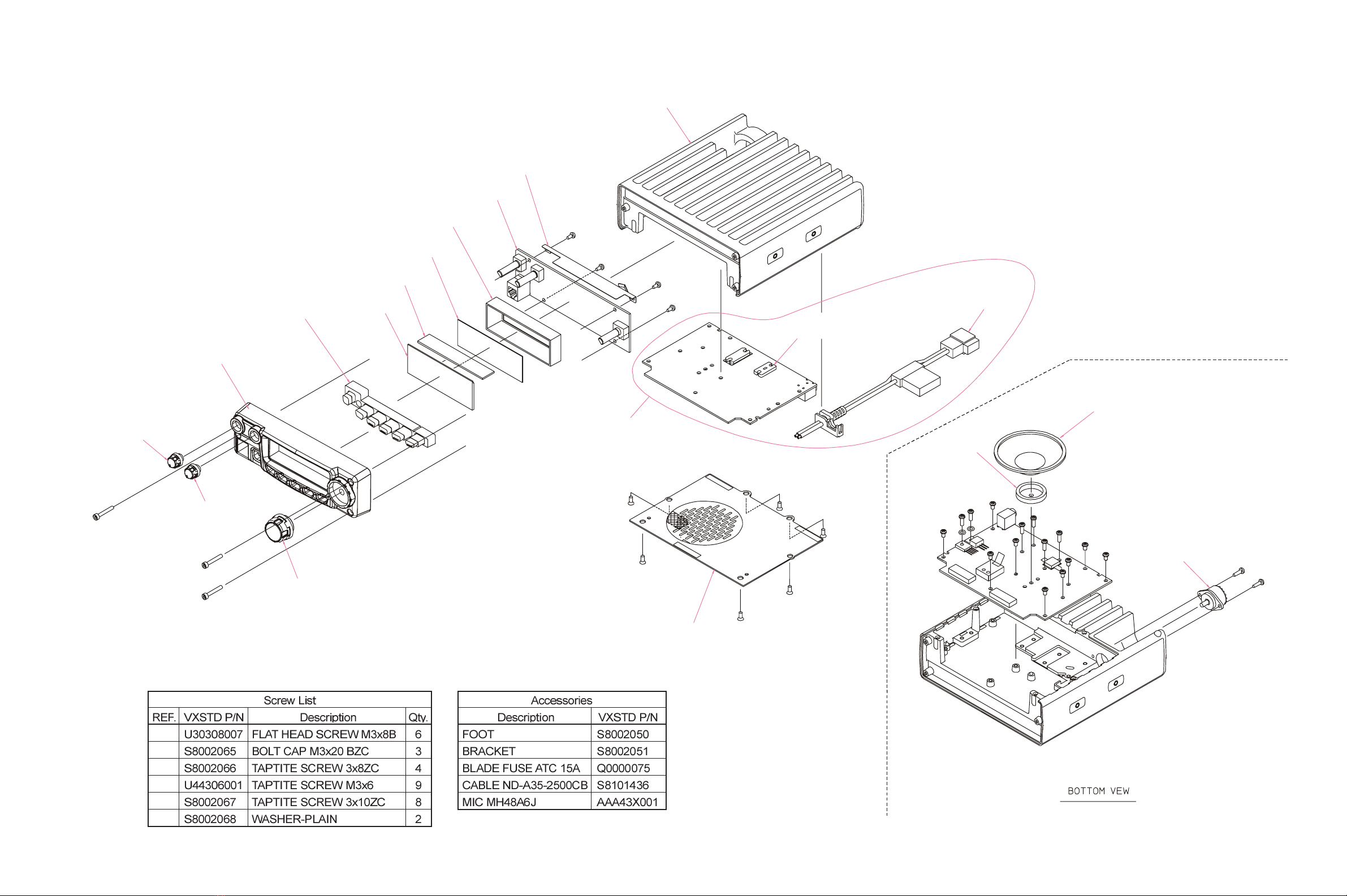
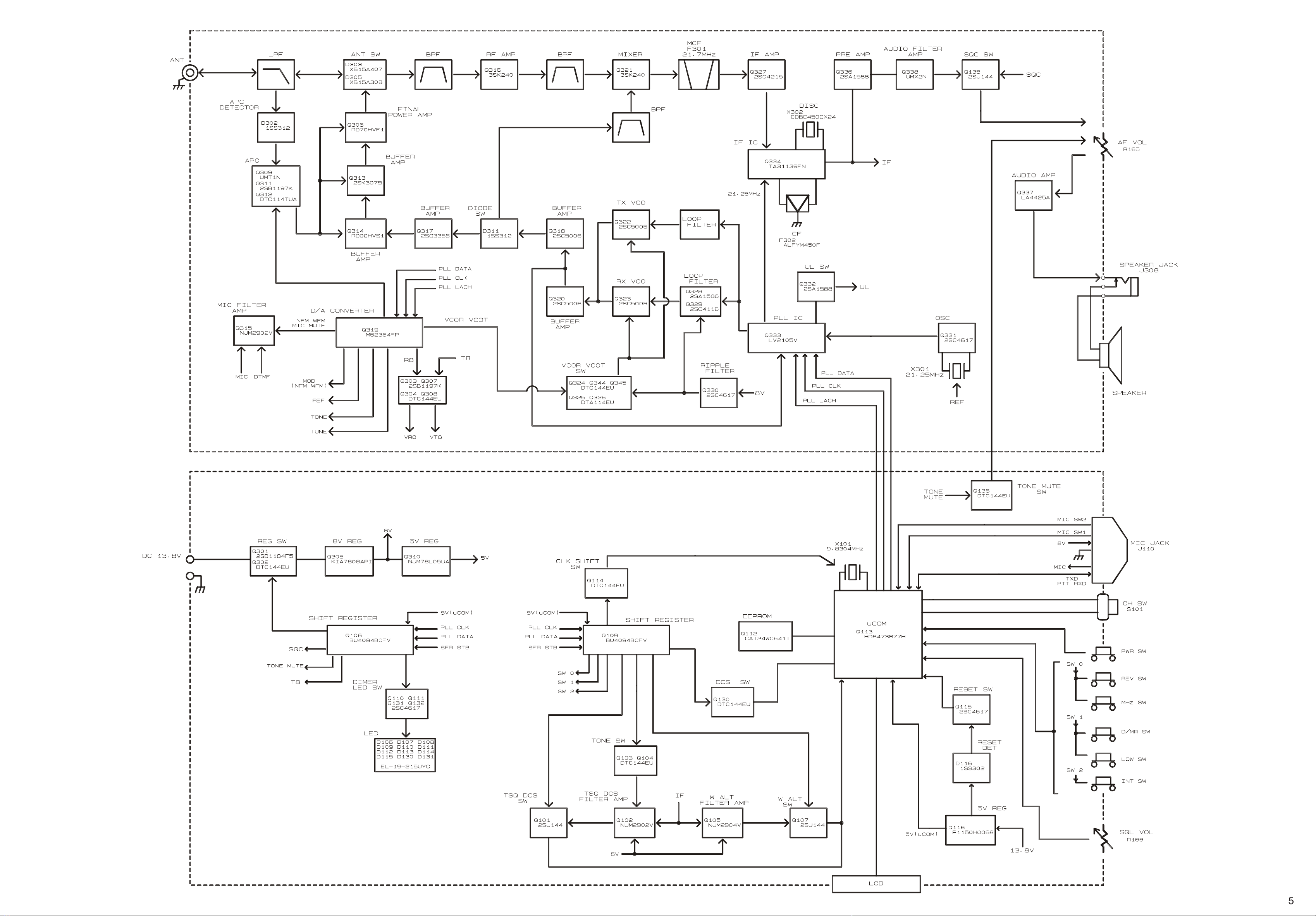
Yaesu FT-2800M Manual

1
Introduction
This manual provides technical information necessary for servicing the FT-2800M FM Transceiver.
Servicing this equipment requires expertise in handling surface-mount chip components. Attempts by non-qualified per-
sons to service this equipment may result in permanent damage not covered by the warranty, and may be illegal in some
countries.
Two PCB layout diagrams are provided for each double-sided circuit board in the Transceiver. Each side of is referred to
by the type of the majority of components installed on that side (“leaded” or “chip-only”). In most cases one side has only
chip components, and the other has either a mixture of both chip and leaded components (trimmers, coils, electrolytic
capacitors, ICs, etc.), or leaded components only.
While we believe the technical information in this manual to be correct, VERTEX STANDARD assumes no liability for
damage that may occur as a result of typographical or other errors that may be present. Your cooperation in pointing out
any inconsistencies in the technical information would be appreciated.
©2007 VERTEX STANDARD CO., LTD. EH014N90B
Technical Supplement
Specifications..................................................... 2
Exploded View & Miscellaneous Parts ........... 3
Block Diagram .................................................. 5
Circuit Description .......................................... 7
Alignment .......................................................... 9
Contents
Board Unit (
Schematics, Layouts & Parts
)
μCOM Unit /RF Unit Circuit Diagram ......................... 13
μCOM Unit Parts Layout .............................................. 15
μCOM Unit Parts List ................................................... 19
RF Unit Parts Layout .................................................... 23
RF Unit Parts List ......................................................... 29
PWR MHz REV LOW D/MR
FM TRANSCEIVER
FT-2800M
VERTEX STANDARD CO., LTD.
4-8-8 Nakameguro, Meguro-Ku, Tokyo 153-8644, Japan
VERTEX STANDARD
US Headquarters
10900 Walker Street, Cypress, CA 90630, U.S.A.
YAESU EUROPE B.V.
P.O. Box 75525, 1118 ZN Schiphol, The Netherlands
YAESU UK LTD.
Unit 12, Sun Valley Business Park, Winnall Close
Winchester, Hampshire, SO23 0LB, U.K.
VERTEX STANDARD HK LTD.
Unit 5, 20/F., Seaview Centre, 139-141 Hoi Bun Road,
Kwun Tong, Kowloon, Hong Kong
VERTEX STANDARD (AUSTRALIA)PTY., LTD.
Normanby Business Park, Unit 14/45 Normanby Road
Notting Hill 3168, Victoria, Australia

2
Specifications
General
Frequency Range: Tx 144 - 146 MHz or 144 - 148 MHz
Rx 144 - 146 MHz or 137 - 174 MHz
Channel Step: 5/10/12.5/15/20/25/50/100 kHz
Standard Repeater Shift: ±600 kHz
Frequency Stability: Better than ±10 ppm [–4 °F to +140 °F (–20 °C to +60 °C)]
Modes of Emission: F2/F3
Antenna Impedance: 50 Ohms, unbalanced
Supply voltage: 13.8 V DC ±15%, negative ground
Current Consumption (typical): Rx: less than 0.7 A, less than 0.3 A (squelched)
Tx: 10 A (65 W)/7 A (25 W)/5 A (10 W)/4 A (5 W)
Operating Temperature Range: –4° F to +140° F (–20° C to +60° C)
Case Size (WxHxD): 6.3” x 2.0” x 7.3” (160 x 50 x 185 mm) (w/o knobs)
Weight (Approx.): 4.0 lb (1.8 kg)
Transmitter
Output Power: 65 W/25 W/10 W/5 W
Modulation Type: Variable Reactance
Maximum Deviation: ±5 kHz/±2.5 kHz
Spurious Radiation: Better than –60 dB
Microphone Impedance: 2000 Ohms
Receiver
Circuit Type: Double Conversion Superheterodyne
Ifs: 21.7 MHz & 450 kHz
Sensitivity (for 12dB SINAD): Better than 0.2 μV
Selectivity (–6/–60dB): 12 kHz/28 kHz
IF Rejection: Better than 70 dB
Image Rejection: Better than 70 dB
Maximum AF Output: 3 W into 4 Ohms @10 % THD
Specifications subject to change without notice or obligation. Specifications guaranteed only within Amateur band

3
Exploded View & Miscellaneous Parts
S8101427
CONNECTOR
S8002063
CAP-SP
S8002058
COVER-BOTTOM ASSY
S8002052
KNOB-VOL
S8002053
KNOB-DIAL
S8002052
KNOB-VOL
S8101433
SPEAKER
S8101435
CABLE
(with BLADE FUSE)
S8002064
SPACER
S8002055
PLATE-EARTH
S8002057
CASE-MAIN
S8002056
REFLECTOR
µCOM Unit
S8002060
FILTER-LCD
S8002061
CONNECT-LCD
S8002059
CASE-FRONT
S8101434
LCD
S8002062
BUTTON
RF ASSY

4
Exploded View & Miscellaneous Parts
Note

Block Diagram

Block Diagram
Note

7
Circuit Description
Reception and transmission are switched by “RX” and
“TX” lines from the microprocessor unit (MPU). The re-
ceiver uses double-conversion superheterodyne circuitry,
with a 21.7 MHz 1st IF and 450 kHz 2nd IF. The 1st lo-
cal, produced by a PLL synthesizer, yields the 21.7 MHz
1st IF.
The 2nd local uses a 21.250 MHz (21.7 MHz - 450 kHz)
signal generated by a crystal oscillator. The 2nd mixer
and other circuits use a custom IC to convert and amplify
the 2nd IF, and detect FM to obtain demodulated signals.
During transmit, the PLL synthesizer oscillates at the de-
sired frequency directly, for amplification to obtain RF
power output. During transmit, voice modulation and
CTCSS (or DCS) modulation are applied to this synthe-
sizer. Transceiver functions, such as TX/RX control, PLL
synthesizer settings, and channel programming, are con-
trolled using the MPU.
Receiver
Incoming RF signals from the antenna connector are de-
livered to the RF Unit, and pass through a lowpass filter
(LPF) consisting of coils L303, L305, and L307, capaci-
tors C303, C309, C310, and C316, and antenna switching
diodes D305 and D306 (Both MA111) for delivery to the
receiver front end.
Signals within the frequency range of the transceiver are
then passed through a varactor-tuned bandpass filter con-
sisting of diodes D308, D322, D310 and D323 (all
HVC3508), and coils L334, L335, L320 and L322 and
associated circuitry before RF amplification by Q316
(3SK240).
The amplified RF signal is then bandpass filtered again
by varactor-tuned resonators consisting of diodes D312,
D324, D313 and D325 (all HVC3508), and coils L336,
L337, L325 and L327 and associated circuitry, to ensure
pure in-band input to 1st mixer Q321 (3SK240).
Buffered output from the VCO Unit is amplified by Q318
(2SC5006) and lowpass-filtered by L339, C414, and
C413, to provide a pure 1st local signal between 112.3
and 152.3 MHz, which is delivered to the 1st mixer.
The 21.7 MHz 1st mixer product then passes through dual
monolithic crystal filter F301 (7.5 kHz BW), and is am-
plified by Q327 (2SC4215Y) and delivered to the input
of the FM IF subsystem IC Q334 (TA31136FN).
This IC contains the 2nd mixer, 2nd local oscillator, lim-
iter amplifier, FM detector, noise amplifier, S-meter am-
plifier and squelch gates.
The 2nd local in the IF-IC is produced from crystal X302
(21.250 MHz), and the 1st IF is converted to 450 kHz by
the 2nd mixer and stripped of unwanted components by
ceramic filter F302. After passing through a limiter am-
plifier, the signal is demodulated by the FM detector.
Demodulated receive audio from the IF-IC is amplified
by Q336 (2SA1588Y) and Q338 (UMX2M). After vol-
ume adjustment by the AF power amplifier Q337
(LA4425A), the audio signal is passed to the optional
headphone or 8-ohm loudspeaker.
PLL Synthesizer
The 1st local maintains stability from the PLL synthesiz-
er by using a 21.250 MHz reference signal from crystal
X301. PLL synthesizer IC Q333 (LV2105V) consists of
a prescaler, reference counter, swallow counter, program-
mable counter, a serial data input port to set these counters
based on external data, a phase comparator, and a charge
pump.
The PLL-IC divides the 21.250 MHz reference signal by
4,250 using the reference counter (5.0 kHz comparison
frequency). The VCO output is divided by the prescaler,
swallow counter and programmable counter. These two
signals are compared by the phase comparator and ap-
plied to the charge pump. A voltage proportional to their
phase difference is delivered to the low-pass filter circuit,
then fed back to the VCO as a voltage with phase error,
controlling and stabilizing the oscillating frequency. This
synthesizer also operates as a modulator during transmit.
The RX VCO is comprised of Q323 (2SC5006) and
D314/D326 (Both 1SV282), and oscillates at 21.7 MHz
during receive.
The TX VCO is comprised of Q322 (2SC5006) and
D316/D327 (Both 1SV282) and oscillates at the funda-
mental frequency during transmit, with direct frequency-
modulation using varactor diode D315 (1SV214).
The VCO output passes through buffer amplifier Q320
(2SC5005), and a portion is fed to the PLL IC, and at the
same time is amplified by Q318 (2SC5006) to obtain
stable output. Synthesizer output is fed to the 1st mixer
by diode switch D311 (1SS321) during receive, and to
pri-drive amplifier Q317 (2SC3356) for transmit.
The reference oscillator feeds the PLL synthesizer, and is
composed of crystal X301 (21.250 MHz) and transmit
(DCS) modulation circuit D317 (HVC350B).
The VCO DC supply is regulated by Q330 (2SC4617).

8
Circuit Description
Transmitter
The speech signal from the microphone is delivered via
the MIC Jack to the RF Unit; after passing through Q315
(NJM2902V) which consists of amplifier, pre-emphasis,
limiter (IDC instantaneous deviation control) and lowpass
filter, to Q319 (M6364FP) which is adjusted for opti-
mum deviation level and delivered to the TX VCO Q322.
The speech signal from the microphone and CTCSS are
FM modulated by the TX VCO of the synthesizer, while
DCS audio is modulated by the reference frequency os-
cillator of the synthesizer.
Synthesizer output, after passing through diode switch
D311 (1SS321), is amplified by pri- drivers Q317
(2SC3356) and Q314 (RD00HVS1), driver Q313
(2SK3075), and power amplifier Q305 (RD70HVS1)
to obtain full RF output. The RF energy then passes
through antenna switch D303 (XB15A407) and a low-
pass filter circuit and finally to the antenna connector.
RF output power from the final amplifier is sampled by
C318 and C324 and is rectified by D302 (1SS321).
The resulting DC is fed through Automatic Power Con-
troller Q309 (UMT1N), Q312 (DTC114), and Q311
(2SB1197) to transmitter RF amplifier Q305 and is used
to provide control of the power output.
Generation of spurious products by the transmitter is min-
imized by the fundamental carrier frequency being equal
to the final transmitting frequency, modulated directly in
the transmit VCO.
Additionally harmonic suppression is provided by a low-
pass filter consisting of L303, L305, C303, C309, C310,
and C316, resulting in more than 60 dB of harmonic sup-
pression prior to delivery of the RF

9
Alignment
Introduction and Precautions
The FT-2800M has been carefully aligned at the factory
for the specified performance at the 144 MHz amateur
band. Realignment should therefore not be necessary ex-
cept in the event of a component failure. All component
replacement and service should be performed only by an
authorized Vertex Standard representative, or the warranty
policy may be voided.
The following procedures cover the sometimes critical and
tedious adjustments that are not normally required once
the transceiver has left the factory. However, if damage
occurs and some parts are replaced, realignment may be
required. If a sudden problem occurs during normal oper-
ation, it is likely due to component failure; realignment
should not be done until after the faulty component has
been replaced.
We recommend that servicing be performed only by au-
thorized Vertex Standard service technicians who are ex-
perienced with the circuitry and fully equipped for repair
and alignment. Therefore, if a fault is suspected, contact
the dealer from whom the transceiver was purchased for
instructions regarding repair. Authorized Vertex Standard
service technicians realign all circuits and make complete
performance checks to ensure compliance with factory
specifications after replacing any faulty components.
Those who do undertake any of the following alignments
are cautioned to proceed at their own risk. Problems caused
by unauthorized attempts at realignment are not covered
by the warranty policy. Also, Vertex Standard must re-
serve the right to change circuits and alignment proce-
dures in the interest of improved performance, without
notifying owners.
Under no circumstances should any alignment be attempt-
ed unless the normal function and operation of the trans-
ceiver are clearly understood, the cause of the malfunc-
tion has been clearly pinpointed and any faulty compo-
nents replaced, and the need for realignment determined
to be absolutely necessary.
Required Test Equipment
The following test equipment (and thorough familiarity
with its correct use) is necessary for complete realign-
ment. Correction of problems caused by misalignment
resulting from use of improper test equipment is not cov-
ered under the warranty policy. While most steps do not
require all of the equipment listed, the interactions of some
adjustments may require that more complex adjustments
be performed afterwards. Do not attempt to perform only
a single step unless it is clearly isolated electrically from
all other steps. Have all test equipment ready before be-
ginning, and follow all of the steps in a section in the
order presented.
Regulated DC Power Supply: adjustable from 10 to 17
VDC, 15 A
RF Signal Generator with calibrated output level at
200 MHz
Frequency Counter: ±0.1 ppm accuracy at 200 MHz
AF Signal Generator
SINAD Meter
Deviation Meter (linear detector)
AF Milivoltmeter
AF Dummy Load: 8-Ohm, 5 W
DC Voltmeter: high impedance
Inline Wattmeter with 5% accuracy at 200 MHz
50-Ohm non-reactive Dummy Load:
100 watts at 200 MHz
VHF Sampling Coupler
Set up the test equipment as shown for the transceiver
alignment, and apply 13.8 VDC power to the transceiver.
Alignment Preparation & Precautions
A dummy load and inline wattmeter must be connected to
the antenna jack in all procedures that call for transmis-
sion, except where specified otherwise. Correct alignment
is not possible with an antenna. After completing one step,
read the following step to determine whether the same
test equipment will be required. If not, remove the test
equipment (except dummy load and wattmeter, if connect-
ed) before proceeding.
Correct alignment requires that the ambient temperature
in the repair shop be the same as that of the transceiver
and test equipment, and that this temperature be held con-
stant between 68 °C and 86 °F (20 °C ~ 30 °C). When the
transceiver is brought into the shop from hot or cold air it
should be allowed some time for thermal equalization with
the environment before alignment. If possible, alignments
should be made with oscillator shields and circuit boards
firmly affixed in place. Also, the test equipment must be
thoroughly warmed up before beginning.
Notes: Signal levels in dB referred to in alignment are
based on 0 dBμ= 0.5 μV.

10
Entering the Alignment mode
Alignment of the FT-2800M is performed using a front-
panel software-based procedure. To perform alignment
of the transceiver, it must first be placed in the “Align-
ment Mode,” in which the adjustments will be made and
then stored into memory.
To enter the Alignment mode:
1. Press and hold in the [LOW]key and [D/MR]key
while turning the radio on. Once the radio is on, re-
lease these two keys.
2. Press and hold the [MHz]key for one second to acti-
vate the “Set” (Menu) mode.
3. Rotate the DIAL knob to select “35 D/ASMT,” then
press the [MHz]key.
4. You will now note the appearance of “REF” on the
display, this signifies that the transceiver is now in
the “Alignment mode.”
PLL Reference Frequency (REF)
1. Tune the transceiver to 146.000 MHz.
2. Set the transceiver to Alignment mode, then rotate the
DIAL knob to set the Alignment parameter to “REF.”
3. Press the PTT switch to activate the transmitter, and
press the [REV]or [D/MR]key, as needed, so that
the counter frequency reading is 146.000 MHz.
4. Press and hold the [LOW]key for one second to save
the new setting.
5. Press and hold the [MHz]key for one second to exit
to the normal operation.
PLL VCO
1. Connect the DC voltmeter to TP-RVC on the RF Unit.
2. Tune the frequency to 146.000 MHz.
3. Adjust L330 on the RF Unit for 1.5 V on the DC volt-
meter.
4. Connect the DC voltmeter to TP-TVC on the RF Unit.
5. Press the PTT switch to activate the transmitter, and
adjust L329 on the RF Unit for 1.3 V on the DC volt-
meter.
RF Front-end Tuning
(TUN137/TUN146/TUN160/TUN173)
1. Connect the DC voltmeter to the Test Point (RSSI:
Pin 6 of J307) on the RF Unit.
2. Tune the transceiver to 137.050 MHz.
3. Set the transceiver to Alignment mode, then rotate the
DIAL knob to set the Alignment parameter to
“TUN137.”
4. Inject a 137.050 MHz signal at a level of –5 dBμ(with
1 kHz modulation @ ±3.5 kHz deviation) from the
RF Signal Generator.
5. Press the [REV]or [D/MR]key for maximum deflec-
tion of the DC voltmeter.
6. Press and hold the [LOW]key for one second to save
the new setting, then press and hold the [MHz]key
for one second to exit to the normal operation.
7. Tune the transceiver to 146.050 MHz.
8. Set the transceiver to Alignment mode, then rotate the
DIAL knob to set the Alignment parameter to
“TUN146.”
Alignment
RF UNIT ALIGNMNT POINTS
L329
RSSI
L330
TP-TVC
TP-RVC

11
9. Inject a 146.050 MHz signal at a level of –5 dBμ(with
1 kHz modulation @ ±3.5 kHz deviation) from the
RF Signal Generator.
10. Press the [REV]or [D/MR]key for maximum
def4lection of the DC voltmeter and maximum de-
flection of the SINAD meter.
11. Press and hold the [LOW]key for one second to save
the new setting, then press and hold the [MHz]key
for one second to exit to the normal operation.
12. Tune the transceiver to 160.050 MHz.
13. Set the transceiver to Alignment mode, then rotate the
DIAL knob to set the Alignment parameter to
“TUN160.”
14. Inject a 160.050 MHz signal at a level of –5 dBμ(with
1 kHz modulation @ ±3.5 kHz deviation) from the
RF Signal Generator.
15. Press the [REV]or [D/MR]key for maximum deflec-
tion of the DC voltmeter voltmeter at the higher side
of the bandpass filter peaks.
16. Press and hold the [LOW]key for one second to save
the new setting, then press and hold the [MHz]key
for one second to exit to the normal operation.
17. Tune the transceiver to 173.050 MHz.
18. Set the transceiver to Alignment mode, then rotate the
DIAL knob to set the Alignment parameter to
“TUN173.”
19. Inject a 173.050 MHz signal at a level of –5 dBμ(with
1 kHz modulation @ ±3.5 kHz deviation) from the
RF Signal Generator.
20. Press the [REV]or [D/MR]key for maximum deflec-
tion of the DC voltmeter at the higher side of the
bandpass filter peaks.
21. Press and hold the [LOW]key for one second to save
the new setting, then press and hold the [MHz]key
for one second to exit to the normal operation.
S-Meter Sensitivity (SMTL 10/SMTL 2)
1. Set the transceiver to Alignment mode, then rotate the
DIAL knob to set the Alignment parameter to “SMTL
10.”
2. Inject a 146.050 MHz signal at a level of +25 dBμ
(with 1 kHz modulation @ ±3.5 kHz deviation) from
the RF Signal Generator.
3. Press and hold the [LOW]key for one second to save
the new setting.
4. Rotate the DIAL knob one click to clockwise to set
the Alignment parameter to “SMTL 2.”
5. Reduce the RF Signal Generator output level to –5
dBμ.
6. Press and hold the [LOW]key for one second to save
the new setting.
7. Press and hold the [MHz]key for one second to exit
to the normal operation.
TX Power Output
(TXPW H/TXPW M/TXPW L2/TXPW L1)
1. Tune the transceiver to 146.000 MHz, and set the
Transmitter Power Level to “HIGH.”
2. Set the transceiver to Alignment mode, then rotate the
DIAL knob to set the Alignment parameter to “TXPW
H.”
3. Press the PTT switch to activate the transmitter, and
press the [REV]or [D/MR]key for 65 Watts on the
wattmeter, and confirm that supply current remains
below 12.5 A.
4. Press and hold the [LOW]key for one second to save
the new setting, then rotate the DIAL knob one click
to clockwise to set the Alignment parameter to
“TXPW M.”
5. Press the PTT switch to activate the transmitter, and
press the [REV]or [D/MR]key for 25 Watts on the
wattmeter, and confirm that supply current remains
below 7.5 A.
6. Press and hold the [LOW]key for one second to save
the new setting, then rotate the DIAL knob one click
to clockwise to set the Alignment parameter to
“TXPWL2.”
7. Press the PTT switch to activate the transmitter, and
press the [REV]or [D/MR]key for 10 Watts on the
wattmeter, and confirm that supply current remains
below 5 A.
8. Press and hold the [LOW]key for one second to save
the new setting, then rotate the DIAL knob one click
to clockwise to set the Alignment parameter to
“TXPWL1.”
9. Press the PTT switch to activate the transmitter, and
press the [REV]or [D/MR]key for 5 Watts on the
wattmeter, and confirm that supply current remains
below 4 A.
10. Press and hold the [LOW]key for one second to save
the new setting, then press and hold the [MHz]key
for one second to exit to the normal operation.
Alignment

12
TX Deviation (MODWFM/MODNFM)
1. Tune the transceiver to 146.000 MHz.
2. Inject a 1 kHz audio tone at a level of 60 mV from the
Audio Generator.
3. Set the transceiver to Alignment mode, then rotate the
DIAL knob to set the Alignment parameter to
“MODWFM.”
4. Press the PTT switch to activate the transmitter, and
press the [REV]or [D/MR]key so that the deviation
meter reading is 4.2 kHz.
5. Press and hold the [LOW]key for one second to save
the new setting, then rotate the DIAL knob one click
to clockwise to set the Alignment parameter to
“MODNFM.”
6. Press the PTT switch to activate the transmitter, and
press the [REV]or [D/MR]key so that the deviation
meter reading is 2.1 kHz.
7. Press and hold the [LOW]key for one second to save
the new setting, then press and hold the [MHz]key
for one second to exit to the normal operation.
CTCSS TX Deviation (TONE W/TONE N)
1. Tune the transceiver to 146.000 MHz.
2. Set the CTCSS tone to 100 Hz.
Press and hold the [MHz]key for one second to
activate the “Set” (Menu) mode.
Rotate the DIAL knob to select “27 SQ TNF.”
Press the [MHz]key momentarily, then rotate the
DIAL knob to select to 100.0 (Hz).
Press and hold the [MHz]key for one second to
exit to the normal operation
3. Set the transceiver to Alignment mode, then rotate the
DIAL knob to set the Alignment parameter to “TONE
W.”
4. Press the PTT switch to activate the transmitter, and
press the [REV]or [D/MR]key so that the deviation
meter reading is 0.6 kHz.
5. Press and hold the [LOW]key for one second to save
the new setting, then rotate the DIAL knob one click
to counter clockwise to set the Alignment parameter
to “TONE N.”
6. Press the PTT switch to activate the transmitter, and
press the [REV]or [D/MR]key so that the deviation
meter reading is 0.3 kHz.
7. Press and hold the [LOW]key for one second to save
the new setting, then press and hold the [MHz]key for
one second to exit to the normal operation.
Alignment

μCOM Unit /RF Unit Circuit Diagram

μCOM Unit /RF Unit Circuit Diagram
Note

15
ABCDEFG
1
2
abcdefg
1
2
Side A
Side B
2SJ144Y (VY)
(Q101, 107, 135)
NJM2902V
(Q102)
DTC144EU (26)
(Q103, 104, 130, 136, 137)
NJM2904V
(Q105)
BU4094BCFV
(Q106, 109)
2SC4617R (BR)
(Q110, 111, 115, 130, 132)
CAT24WC64JI
(Q112)
1SS302 (C3)
(D101, 102, 116, 118)
DAP202U (P)
(D104, 105)
HD6473877H
(Q113)
μCOM Unit Parts Layout (Lot. 1 ~ 15)

16
μCOM Unit Parts Layout (Lot. 16 ~ 57)
ABCDEFG
1
2
abcdefg
1
2
Side A
Side B
2SJ144Y (VY)
(Q101, 107, 135)
NJM2902V
(Q102)
DTC144EU (26)
(Q103, 104, 130, 136, 137)
NJM2904V
(Q105)
BU4094BCFV
(Q106, 109)
2SC4617R (BR)
(Q110, 111, 115, 130, 132)
CAT24WC64JI
(Q112)
1SS302 (C3)
(D101, 102, 116, 118)
DAP202U (P)
(D104, 105)
HD6473877H
(Q113)
VR IN
VR GND
VR OUT
SQL VR
DCS
DSC DET
USER P
REG SW
PLL LACH
PLL DATA
PLL CK
UL
TONE OUT
13.8V
5V
RSSI
TEMP
8V
MIC
GND
DTMF
T8
MIC GND
D/A STB
R165 R166
S101
J110
R190
D112
D111
D110
D115
D114
D113
D130
D131
D106
D107
D109
D108
DTMF
GND
MIC
8V
TEMP
RS S I
5V
13.8V
TONE OUT
UL
PLL CK
PLL DATA
PLL LACH
REG SW
USER P
DSC DET
DCS
SQL VR
VR OUT
VR GND
VR IN
T8
MIC GND
D/A STB
Q113
R114
C114
C119
C132
R167
R146
R192
R191
R184
R189
R183
R182
C151
C150
R180
Q109 Q106
Q112
Q105
Q102
Q115
Q116
X101
R148
Q135
R201
C155
C161
R209
R151
R139
R136
R1 3 7
R138
L104
L106
C124
C122
C123
L101
J109
L102
L105
R181
J101
D103
C131
C126
R142
Q130
C128
C163
R143
L103
C125
R134
R135
C129
R144
R153
R164
R163
R162
C130
R145
C138
D118
C152
R187
C112
R121
R123
C120
C121
R124
R132
R160
R150
C133
C135
D116
R158
D117
C137
C134
D105
R133
R131
Q111
Q110
R105
R107
C110
C106
R106
R204
R188
R102
C1 1 8
C107
C113
R225
R113
C105
C109
R202
C103
R115
D137
R140
D104
C104
R161
R112 C158
R141
R111
C108
C116
C167
C156
R122
C136
R203
C159
R206
R116
C111
R119
R110
R104
C102
R109
R126
C160
C101
R108
R101
R186
R185
Q101
Q132
Q131
D102
D101
R152
R149
R147
R205
R193
Q103
R212
Q104
Q107
R128
C115
R228
R207
Q136
R208
R211
C127
Q137
R210
R200
C117
C164
D135
C165
R221
R220
R223
R120

17
μCOM Unit Parts Layout (Lot. 58 ~)
ABCDEFG
1
2
abcdefg
1
2
Side A
Side B
2SJ144Y (VY)
(Q101, 107, 135)
NJM2902V
(Q102)
DTC144EU (26)
(Q103, 104, 130, 136, 137)
NJM2904V
(Q105)
BU4094BCFV
(Q106, 109)
2SC4617R (BR)
(Q110, 111, 115, 130, 132)
CAT24WC64JI
(Q112)
1SS302 (C3)
(D101, 102, 116, 118)
DAP202U (P)
(D104, 105)
HD6473877H
(Q113)

18
Note

19
REF DESCRIPTION VALUE V/W TOL. MFR'S DESIG VXSTD P/N VERS. LOT
SIDE
LAY ADR
μCOM Unit Parts List
PCB with Components CS1806001 TYPE A2
CS1806002 TYPE A1
CS1806003 TYPE A3
CS1806004 TYPE B1
CS1806005 TYPE B2
CS1806006 TYPE B3
Printed Circuit Board S8101505 1-
FR0142500 57-
C 101 CHIP CAP. 1uF 10V B GRM188B11A105KA61D S8101390 1-
C 102 CHIP CAP. 0.1uF 16V B GRM188B11C104KA01D K22124805 1-
C 103 CHIP CAP. 0.015uF 50V B GRM188B11H153KA01D S8101391 1-
C 104 CHIP CAP. 0.1uF 16V B GRM188B11C104KA01D K22124805 1-
C 105 CHIP CAP. 0.0027uF 50V B GRM188B11H272KA01D K22174829 1-
C 106 CHIP CAP. 390pF 50V B GRM188B11H391KD01D K22174804 1-
C 107 CHIP CAP. 0.0068uF 50V B GRM188B11H682KA01D K22174834 1-
C 108 CHIP CAP. 0.001uF 50V B GRM188B11H102KA01D K22174821 1-
C 109 CHIP CAP. 0.001uF 50V B GRM188B11H102KA01D K22174821 1-
C 110 CHIP CAP. 680pF 50V B GRM188B11H681KA01D K22174807 1-
C 111 CHIP CAP. 0.015uF 50V B GRM188B11H153KA01D S8101391 1-
C 112 AL.ELECTRO.CAP. 100uF 6.3V EMV-6R3ADA101MF55G S8101399 1-
C 113 CHIP CAP. 0.0068uF 50V B GRM188B11H682KA01D K22174834 1-
C 114 CHIP CAP. 0.001uF 50V B GRM188B11H102KA01D K22174821 1-
C 115 CHIP CAP. 0.001uF 50V B GRM188B11H102KA01D K22174821 1-
C 116 CHIP CAP. 0.001uF 50V B GRM188B11H102KA01D K22174821 1-
C 117 CHIP CAP. 0.001uF 50V B GRM188B11H102KA01D K22174821 1-
C 118 CHIP CAP. 0.027uF 16V R GRM188R11C273KA01D K22124802 1-
C 119 AL.ELECTRO.CAP. 10uF 16V EMV-160ADA100MD55G S8101398 1-
C 120 CHIP CAP. 0.001uF 50V B GRM188B11H102KA01D K22174821 1-
C 121 CHIP CAP. 0.001uF 50V B GRM188B11H102KA01D K22174821 1-
C 125 CHIP CAP. 0.001uF 50V B GRM188B11H102KA01D K22174821 1-
C 126 CHIP CAP. 18pF 50V CH GRM1882C1H180JA01D K22174217 1-
C 127 CHIP CAP. 0.001uF 50V B GRM188B11H102KA01D K22174821 1-
C 128 CHIP CAP. 6pF 50V CH GRM1882C1H6R0DZ01D K22174207 1-
C 129 CHIP CAP. 0.01uF 50V B GRM188B11H103KA01D K22174823 1-
C 130 CHIP CAP. 0.001uF 50V B GRM188B11H102KA01D K22174821 1-
C 131 CHIP CAP. 1uF 10V B GRM188B11A105KA61D S8101390 1-
C 132 CHIP CAP. 1uF 10V B GRM188B11A105KA61D S8101390 1-
C 133 CHIP CAP. 0.001uF 50V B GRM188B11H102KA01D K22174821 1-
C 134 AL.ELECTRO.CAP. 100uF 6.3V EMV-6R3ADA101MF55G S8101399 1-
C 135 CHIP CAP. 0.001uF 50V B GRM188B11H102KA01D K22174821 1-
C 136 CHIP CAP. 0.001uF 50V B GRM188B11H102KA01D K22174821 1-
C 137 AL.ELECTRO.CAP. 100uF 16V UWX1C101MCL1GB S8101395 1-
C 138 CHIP CAP. 0.01uF 50V B GRM188B11H103KA01D K22174823 1-
C 150 CHIP TA.CAP. 10uF 6.3V TEMSVA0J106M-8R K78080027 1-
C 152 CHIP CAP. 0.001uF 50V B GRM188B11H102KA01D K22174821 1-
C 155 CHIP CAP. 0.1uF C1608JB1H104KT S8101503 1-
C 158 CHIP CAP. 0.001uF 50V B GRM188B11H102KA01D K22174821 1-
C 159 CHIP CAP. 0.0047uF 50V B GRM188B11H472KA01D K22174833 1-
C 160 CHIP CAP. 0.001uF 50V B GRM188B11H102KA01D K22174821 1-
C 161 CHIP CAP. 0.01uF 50V B GRM188B11H103KA01D K22174823 1-
C 163 CHIP CAP. 56pF 50V CH GRM1882C1H560JA01D K22174229 1-
C 164 CHIP CAP. 1uF 10V B GRM188B11A105KA61D S8101390 1-
C 165 CHIP CAP. 0.001uF 50V B GRM188B11H102KA01D K22174821 1-
C 167 CHIP CAP. 0.01uF 50V B GRM188B11H103KA01D K22174823 1-
C 168 CHIP CAP. 0.001uF 50V B GRM188B11H102KA01D K22174821 16-
C 169 CHIP CAP. 0.001uF 50V B GRM188B11H102KA01D K22174821 16-
C 170 CHIP CAP. 0.047uF 16V B GRM39B473K16PT K22124804 72-
C 171 CHIP CAP. 0.047uF 16V B GRM39B473K16PT K22124804 72-
D 101 DIODE 1SS302(TE85R.F) G2070088 1-
D 102 DIODE 1SS302(TE85R.F) G2070088 1-
D 103 DIODE MA111-(TX) G2070338 1-
D 104 DIODE DAP202U T106 G2070160 1-
D 105 DIODE DAP202U T106 G2070160 1-
D 106 LED 19-215UYC/S530-A2/TR8 S8101421 1-
D 106 LED 19-215/Y2C-CN1P2/3T S8101644 41-
D 106 LED 19-213/Y2C/CN1P2/3T S8101669 45-
D 107 LED 19-215UYC/S530-A2/TR8 S8101421 1-
D 107 LED 19-215/Y2C-CN1P2/3T S8101644 41-
D 107 LED 19-213/Y2C/CN1P2/3T S8101669 45-
D 108 LED 19-215UYC/S530-A2/TR8 S8101421 1-
D 108 LED 19-215/Y2C-CN1P2/3T S8101644 41-
D 108 LED 19-213/Y2C/CN1P2/3T S8101669 45-
D 109 LED 19-215UYC/S530-A2/TR8 S8101421 1-
D 109 LED 19-215/Y2C-CN1P2/3T S8101644 41-
D 109 LED 19-213/Y2C/CN1P2/3T S8101669 45-
D 110 LED 19-215UYC/S530-A2/TR8 S8101421 1-

20
REF DESCRIPTION VALUE V/W TOL. MFR'S DESIG VXSTD P/N VERS. LOT
SIDE
LAY ADR
μCOM Unit Parts List
D 110 LED 19-215/Y2C-CN1P2/3T S8101644 41-
D 110 LED 19-213/Y2C/CN1P2/3T S8101669 45-
D 111 LED 19-215UYC/S530-A2/TR8 S8101421 1-
D 111 LED 19-215/Y2C-CN1P2/3T S8101644 41-
D 111 LED 19-213/Y2C/CN1P2/3T S8101669 45-
D 112 LED 19-215UYC/S530-A2/TR8 S8101421 1-
D 112 LED 19-215/Y2C-CN1P2/3T S8101644 41-
D 112 LED 19-213/Y2C/CN1P2/3T S8101669 45-
D 113 LED 19-215UYC/S530-A2/TR8 S8101421 1-
D 113 LED 19-215/Y2C-CN1P2/3T S8101644 41-
D 113 LED 19-213/Y2C/CN1P2/3T S8101669 45-
D 114 LED 19-215UYC/S530-A2/TR8 S8101421 1-
D 114 LED 19-215/Y2C-CN1P2/3T S8101644 41-
D 114 LED 19-213/Y2C/CN1P2/3T S8101669 45-
D 115 LED 19-215UYC/S530-A2/TR8 S8101421 1-
D 115 LED 19-215/Y2C-CN1P2/3T S8101644 41-
D 115 LED 19-213/Y2C/CN1P2/3T S8101669 45-
D 116 DIODE 1SS302(TE85R.F) G2070088 1-
D 117 DIODE MA111-(TX) G2070338 1-
D 118 DIODE 1SS302(TE85R.F) G2070088 1-
D 130 LED 19-215UYC/S530-A2/TR8 S8101421 1-
D 130 LED 19-215/Y2C-CN1P2/3T S8101644 41-
D 130 LED 19-213/Y2C/CN1P2/3T S8101669 45-
D 131 LED 19-215UYC/S530-A2/TR8 S8101421 1-
D 131 LED 19-215/Y2C-CN1P2/3T S8101644 41-
D 131 LED 19-213/Y2C/CN1P2/3T S8101669 45-
D 135 DIODE 1SS400 TE61 G2070634 1-
D 137 DIODE 1SS400 TE61 G2070634 1-
J 101 CONNECTOR TKC-M12P-B1 S8101428 1-
J 109 CONNECTOR TKC-M12P-B1 S8101428 1-
J 110 CONNECTOR MJD0606KX06 S8101431 1-
J 115 SHIELD FINGER 0G-603070 S5000244 TYPE B1 19-
J 115 SHIELD FINGER 0G-603070 S5000244 TYPE B2 19-
L 101 M.RFC 4.7uH LK1608 4R7K-T L1690688 1-
L 102 M.RFC 4.7uH LK1608 4R7K-T L1690688 1-
L 103 M.RFC 4.7uH LK1608 4R7K-T L1690688 1-
L 104 M.RFC 4.7uH LK1608 4R7K-T L1690688 1-
L 105 M.RFC 4.7uH LK1608 4R7K-T L1690688 1-
L 106 M.RFC 4.7uH LK1608 4R7K-T L1690688 1-
Q 101 FET 2SJ144Y(TE85R.F) G3701447Y 1-
Q 102 IC NJM2902V-TE1 G1091679 1-
Q 103 TRANSISTOR DTC144EUA T106 G3070041 1-
Q 104 TRANSISTOR DTC144EUA T106 G3070041 1-
Q 105 IC NJM2904V-TE1 G1091677 1-
Q 106 IC BU4094BCFV-E2 G1093527 1-
Q 107 FET 2SJ144Y(TE85R.F) G3701447Y 1-
Q 109 IC BU4094BCFV-E2 G1093527 1-
Q 110 TRANSISTOR 2SC4617 TL R G3346178R 1-
Q 111 TRANSISTOR 2SC4617 TL R G3346178R 1-
Q 112 IC CAT24C64WI-TE13 S8101423 1-
Q 113 IC HD6433877B60H S8101504 1-
Q 113 IC HD6433877B65H G1094163 54-
Q 115 TRANSISTOR 2SC4617 TL R G3346178R 1-
Q 116 IC R1150H006B-T1 S8101422 1-
Q 130 TRANSISTOR DTC144EUA T106 G3070041 1-
Q 131 TRANSISTOR 2SC4617 TL R G3346178R 1-
Q 132 TRANSISTOR 2SC4617 TL R G3346178R 1-
Q 135 FET 2SJ144Y(TE85R.F) G3701447Y 1-
Q 136 TRANSISTOR DTC144EUA T106 G3070041 1-
Q 137 TRANSISTOR DTC144EUA T106 G3070041 1-
Q 137 TRANSISTOR DTC114YUA T106 G3070298 23-
R 101 CHIP RES. 100k 1/16W 5% RMC1/16 104JATP J24185104 1-
R 102 CHIP RES. 15k 1/16W 5% RMC1/16 153JATP J24185153 1-
R 104 CHIP RES. 270k 1/16W 5% RMC1/16 274JATP J24185274 1-
R 105 CHIP RES. 47k 1/16W 5% RMC1/16 473JATP J24185473 1-
R 106 CHIP RES. 68k 1/16W 5% RMC1/16 683JATP J24185683 1-
R 107 CHIP RES. 390k 1/16W 5% RMC1/16 394JATP J24185394 1-
R 108 CHIP RES. 10k 1/16W 5% RMC1/16 103JATP J24185103 1-
R 109 CHIP RES. 0 1/16W 5% RMC1/16 000JATP J24185000 1-
R 110 CHIP RES. 8.2k 1/16W 5% RMC1/16 822JATP J24185822 1-
R 111 CHIP RES. 68k 1/16W 5% RMC1/16 683JATP J24185683 1-
R 112 CHIP RES. 27k 1/16W 5% RMC1/16 273JATP J24185273 1-
R 113 CHIP RES. 390k 1/16W 5% RMC1/16 394JATP J24185394 1-
R 114 CHIP RES. 68k 1/16W 5% RMC1/16 683JATP J24185683 1-
R 115 CHIP RES. 390k 1/16W 5% RMC1/16 394JATP J24185394 1-
R 116 CHIP RES. 390k 1/16W 5% RMC1/16 394JATP J24185394 1-
Other manuals for FT-2800M
3
Table of contents
Other Yaesu Transceiver manuals

Yaesu
Yaesu FTDX-9000D General instructions

Yaesu
Yaesu FTM-3100R Setup guide

Yaesu
Yaesu FTM-400DR Use and care manual

Yaesu
Yaesu FT-7100M User manual

Yaesu
Yaesu FT-50R Manual

Yaesu
Yaesu Mark-V FT-1000MP Installation guide

Yaesu
Yaesu FT-65R User manual

Yaesu
Yaesu VX-7R User manual

Yaesu
Yaesu FT-5200 User manual

Yaesu
Yaesu FT-1900R Manual

Yaesu
Yaesu FT-901DM User manual

Yaesu
Yaesu FT-2500M User manual

Yaesu
Yaesu FT-901DM User manual

Yaesu
Yaesu FT-270R User manual

Yaesu
Yaesu FT-625RD User manual

Yaesu
Yaesu FTM-500DR User manual

Yaesu
Yaesu FT-207R User manual

Yaesu
Yaesu FT-227RB User manual

Yaesu
Yaesu FT-8900R User manual

Yaesu
Yaesu FT-10R User manual