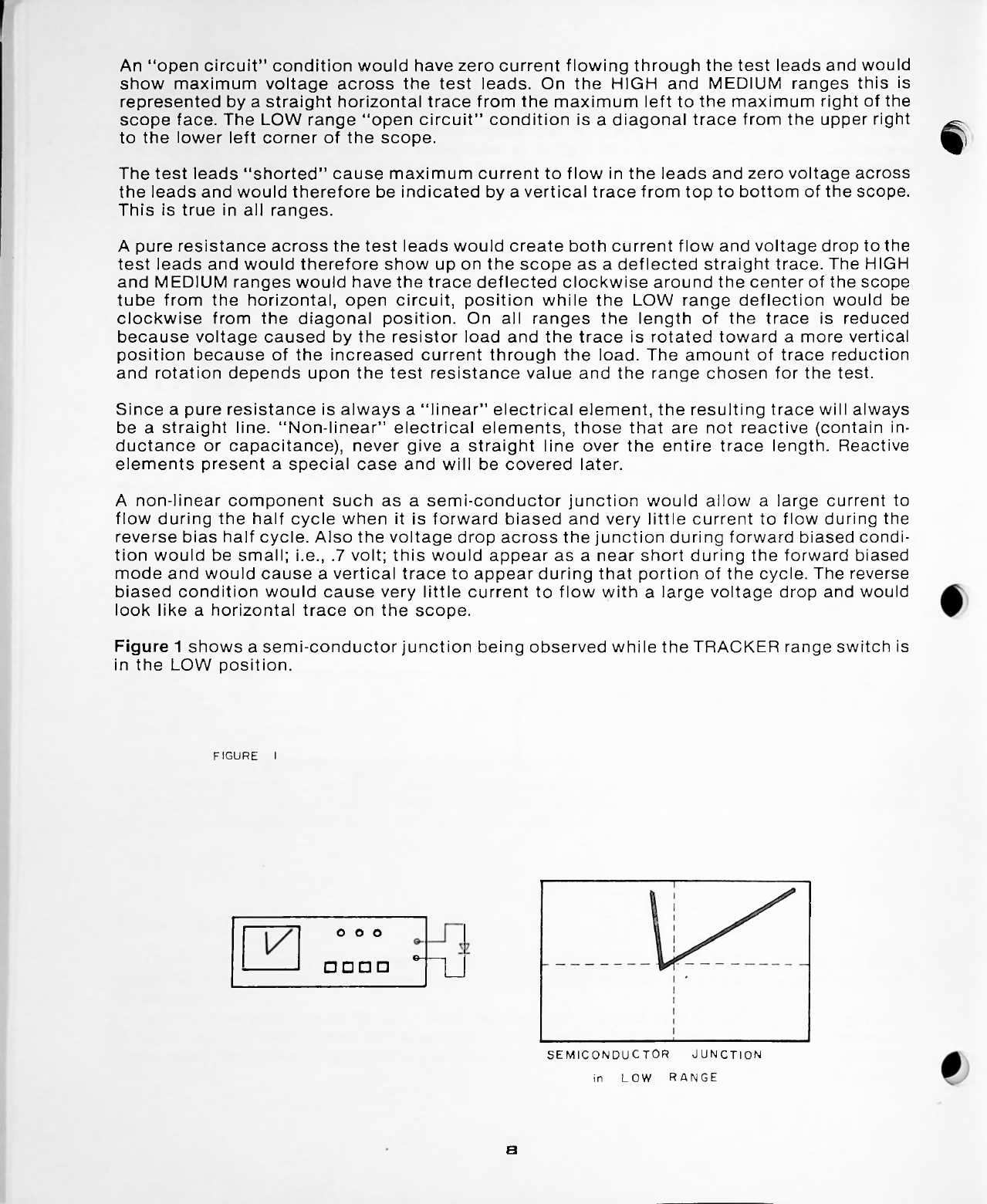
Huntron HTR 1005B-1 User manual

MAINTENANCE
MANUAL
HUNTRON
TRACKER
I
I
ven
:.^\z
huntron
I
med
I
Huntron
Instruments,
Inc.
15123
Pac f c
H ghway
North
Lynnwood,
WA
98036
(206)
743-3171
low
GH/off
high
puack&ir
z
--


TABLE
OF
CONTENTS
WARRANTY
3
I
SPECIFICATIONS
5
GENERAL
DESCRIPTION
6
!
THEORY
OF
OPERATION
CIRCUIT
DESCRIPTION
INTERNAL
SET-UP
AND
ADJUSTMENTS
16
CHARTS
AND
DIAGRAMS
©
COPYRIGHT
1980
—
HUNTRON
INSTRUMENTS
INC.
I
Schematc
D agram
.......................
Waveforms
......................................
P.C.
Board
Voltages
.......................
Component
Parts
L st
...................
Assembl es
L st
.............................
Schematc
Rev s ons
.....................
Exploded
V ew
of
Case
.................
P.C.
Board
Voltages
.......................
Photograph
of
Instrument
Inter or
Tr mpot
Locat on
Chart
.................
Exter or
and
Interor
Drawngs
.
.
.
S gnal
Secton
...................
Inverter
Power
Supply
.
.
.
.
Cathode
Ray
Tube
C rcu ts
Power
Supply
.....................
General
Informaton
.................
The
Test
S gnal
.........................
Test ng
React ve
Components
6
7
10
12
14
15
15
20
25
25
28
30
33
34
35
36
37
38
18
19
19
23
24
TROUBLESHOOTING
General
Informat on
........
Power
Supply
...................
S gnal
Secton
.................
Cathode
Ray
Tube
Secton
Inverter
............................. .


3
LIMITED
WARRANTY
For
a
perod
of
one
year
from
the
date
of
ts
purchase
new
and
undamaged
from
Huntron
Sales,
Inc.,
HUNTRON
INSTRUMENTS,
INC.
wll,
wthout
charge,
repa r
or
replace,
at
ts
opton,
ths
product
f
found
by
t
to
be
defectve
n
materals
or
workmanshp,
and
f
returned
to
HUNTRON
INSTRUMENTS,
INC.
at
ts
factory,
transportaton
prepa d.
Th s
lmted
warranty
s
expressly
cond t oned
upon
the
product
hav ng
been
used
only
n
normal
usage
and
servce
n
accordance
w th
nstructons
of
HUNTRON
INSTRUMENTS,
INC.
and
not
hav ng
been
altered
n
any
way
or
subject
to
msuse,
neglgence
or
damage,
and
not
hav ng
been
repared
or
attempted
to
be
repa red
by
anyone
other
than
HUNTRON
INSTRUMENTS,
INC.
or
ts
author zed
agent.
EXCEPT
FOR
THE
FOREGOING
EXPRESS
WARRANTY
OF
REPAIR
OR
REPLACEMENT
HUNTRON
INSTRUMENTS,
INC.
MAKES
NO
WARRANTY
OF
ANY
KIND,
INCLUDING
BUT
NOT
LIMITED
TO.
ANY
EXPRESS
OR
IMPLIED
WARRANTY
OF
MERCHANTABILITY
OR
FITNESS
FOR
ANY
PARTICULAR
PURPOSE,
AND
HUNTRON
INSTRUMENTS,
INC.
SHALL
NOT
BE
LIABLE
FOR
ANY
DAMAGES,
WHETHER
DIRECT
OR
INDIRECT,
CONSEQUENTIAL
OR
INCIDENTAL.
FORESEEABLE
OR
NOT.
OR
OTHERWISE,
BEYOND
REPAIR
OR
REPLACING
THIS
PRODUCT.
fes
L
Y
few
gW
...................... ..................................................
’
..........
.. ...............
’
So
•V<.rO)
C-
few
few
few


—
=2E
HTR
1005B-1
SPECIFICATIONS
A.C.
Power
Input
Physical
Dimensions
5
pounds
Weight
Signal
Information
Range
5
Low
Range
(Open
test
po nts)
....
Low
Range
(Shorted
test
po nts)
H gh
Med
Low
.8%
nch
,.3
1
/2
nch
11
1
Z?
nch
17
Watts
20
Watts
W dth..
Heght.
Length
Current
R.M.S.
M.A.
.25
.25
92
Current
Peak
M.A.
.7
.7
250
Voltage
P-P
open
circuit
120
40
18
Power
R.M.S.
M.W.
.18
.18
65
Power
Peak
M.W.
.5
.5
250
All
ratngs,
except
P-P
voltages,
are
cond t ons
ex st ng
across
a
s ngle
s l con
d ode
n
the
test
term nals
of
the
Tracker.

<
GENERAL
DESCRIPTION
e
The
RANGE
SWITCH
determ nes
the
voltage
and
mpedance
level
of
the
test
s gnal
source.
THEORY
OF
OPERATION
6
The
current
flow
s
processed
n
such
a
way
as
to
cause
a
vertcal
deflect on
of
the
scope
trace,
wh le
the
voltage
drop
across
the
test
component
causes
a
hor zontal
deflecton
of
the
scope
trace.
The
HUNTRON
TRACKER
appl es
a
test
s gnal
across
two
term nals
of
the
dev ce
be ng
tested.
Th s
test
s gnal
causes
a
current
to
flow
through
the
dev ce
and
a
voltage
drop
across
ts
termnals.
Included
as
standard
equ pment
w th
each
TRACKER
s
a
set
of
spec al
purpose
probes.
The
probe
leads
plug
nto
the
front
panel
test
jacks,
are
f ve
feet
long
and
because
of
spec al
t ps
can
be
used
to
contact
very
small
component
termnals,
as
well
as
small
P.C.
etchngs
w thout
the
danger
of
shortng
adjacent
termnals
and
leads.
The
TRACKER
s
used
to
test
components
n
the
“
power
off
’
’
cond t on
and
can
be
used
to
test
components
mounted
on
pr nted
c rcu t
boards
or
other
“
n-c rcu t
”
cond t ons,
and
w th
components
br dged
by
var ous
types
of
res st ve
values.
The
HUNTRON
TRACKER
s
a
“
Specal
Use
Type
”
of
osc lloscope
and
s gnal
process ng
n
strument
that,
through
v sual
d splay,
determ nes
the
qual ty
of
certan
types
of
electronc
components.
Access
to
the
component
be ng
tested
s
through
a
two
termnal
system
of
test
leads
that
are
placed
across
the
component
under
test.
The
test
leads
are
nserted
nto
the
TRACKER
front
panel.
Dev ces
that
are
normally
tested
by
the
TRACKER
nclude
the
followng:
Sem-conductor
d odes
and
b -polar
transstors;
f eld
effect
transstors;
ntegrated
c rcu t
ch ps
of
the
b -polar
and
M.O.S.
type,
nclud ng
both
d g tal
and
analog;
certan
types
of
capac tors
and
nductors.
Front
panel
controls
nclude
HORIZONTAL
and
VERTICAL
adjustment
of
the
scope
trace,
TRACE
INTENSITY
POWER
SWITCH
and
three
RANGE
SWITCHES.
An
INDICATING
l ght
determ nes
when
the
power
s
“
on
”
.
The
SCOPE
tube
has
a
2Vz
"
x
2"
face
protected
by
a
l ght
ly
smoked
glass
plate.

THE
TEST
SIGNAL
]
7
Th s
s gnal
s
an
80
HZ
modfed
s ne
wave
that
apples
alternately,
pos t ve
and
negatve,
voltages
across
the
component
be ng
tested.
In
an
open
c rcu t
cond t on
the
pos t ve
half
cycle
generates
the
left
s de
trace
on
the
scope
tube;
the
r ght
s de
trace
would
be
the
negat ve
half
cycle.
The
80
HZ
test
s gnal
s
or g nated
n
a
self
contaned
osc llator
and
presented
at
the
front
panel
test
termnals
through
a
s gnal
transformer.
The
transformer
has
the
dual
purpose
of
adjustng
the
test
voltage
level
for
the
var ous
ranges,
as
well
as
selectng
the
mpedance
level
of
the
var ous
ranges.
The
test
s gnal
as
presented
at
the
front
panel,
electrcally
appears
as
though
t
s
be ng
or g nated
by
a
mod f ed
current
generator.
A
true
current
generator
has
nf n te
nternal
m
pedance
and
therefore
ts
current
output
s
not
effected
by
the
load
across
the
generator.
The
TRACKER
test
s gnal
generator
mpedance
s
f n te
and
s
d fferent
for
all
three
ranges.
Figure
2
shows
an
electr cal
equvalent
of
the
generator
secton
and
how
the
voltage
across
the
term nals
affect
the
hor zontal
and
vertcal
deflect on
plates
of
the
scope.
Shown
s
the
symbolc
representaton
of
a
current
generator,
GEN,
w th
a
ser es
nternal
mpedance,
Zgen,
and
a
current
sens ng
po nt,
I.
Across
these
network
elements
are
two
test
po nts,
A
and
B.
Z
gen
—
■e)
B
■'♦20
\
\
\
-20
\.
The
f gure
shows
that
a
test
component
has
not
been
placed
across
the
test
po nts
and
therefore
only
the
hor zontal
voltage
vector
would
appear
at
the
scope.
Zero
current
would
be
flowng,
as
sensed,
po nt
I
and
the
resultant
equ valent
voltage
at
the
vertcal
scope
plate
would
be
zero.
FIGURE
2

c
o
o
o
G-
□
□□□
8
!
JUNCTION
RANGE
A
non-lnear
component
such
as
a
sem -conductor
juncton
would
allow
a
large
current
to
flow
dur ng
the
half
cycle
when
t
s
forward
b ased
and
very
l ttle
current
to
flow
durng
the
reverse
b as
half
cycle.
Also
the
voltage
drop
across
the
juncton
durng
forward
b ased
cond
t on
would
be
small;
.e.,
.7
volt;
th s
would
appear
as
a
near
short
durng
the
forward
b ased
mode
and
would
cause
a
vertcal
trace
to
appear
durng
that
porton
of
the
cycle.
The
reverse
b ased
cond t on
would
cause
very
l ttle
current
to
flow
w th
a
large
voltage
drop
and
would
look
l ke
a
hor zontal
trace
on
the
scope.
S nce
a
pure
res stance
s
always
a
“
lnear
”
electr cal
element,
the
resultng
trace
w ll
always
be
a
stra ght
l ne.
“
Non-lnear
”
electr cal
elements,
those
that
are
not
reactve
(contan
n
ductance
or
capac tance),
never
g ve
a
straght
l ne
over
the
entre
trace
length.
React ve
elements
present
a
spec al
case
and
w ll
be
covered
later.
A
pure
res stance
across
the
test
leads
would
create
both
current
flow
and
voltage
drop
to
the
test
leads
and
would
therefore
show
up
on
the
scope
as
a
deflected
stra ght
trace.
The
HIGH
and
MEDIUM
ranges
would
have
the
trace
deflected
clockwse
around
the
center
of
the
scope
tube
from
the
hor zontal,
open
c rcu t,
pos t on
whle
the
LOW
range
deflecton
would
be
clockwse
from
the
d agonal
pos t on.
On
all
ranges
the
length
of
the
trace
s
reduced
because
voltage
caused
by
the
res stor
load
and
the
trace
s
rotated
toward
a
more
vert cal
pos t on
because
of
the
ncreased
current
through
the
load.
The
amount
of
trace
reducton
and
rotat on
depends
upon
the
test
res stance
value
and
the
range
chosen
for
the
test.
The
test
leads
“
shorted
”
cause
maxmum
current
to
flow
n
the
leads
and
zero
voltage
across
the
leads
and
would
therefore
be
nd cated
by
a
vertcal
trace
from
top
to
bottom
of
the
scope.
Th s
s
true
n
all
ranges.
An
“
open
c rcu t
”
cond t on
would
have
zero
current
flowng
through
the
test
leads
and
would
show
max mum
voltage
across
the
test
leads.
On
the
HIGH
and
MEDIUM
ranges
ths
s
represented
by
a
straght
hor zontal
trace
from
the
max mum
left
to
the
max mum
r ght
of
the
scope
face.
The
LOW
range
“
open
c rcu t
”
cond t on
s
a
d agonal
trace
from
the
upper
r ght
to
the
lower
left
corner
of
the
scope.
u
SEMICONDUCTOR
n
LOW
I
Figure
1
shows
a
sem -conductor
juncton
beng
observed
wh le
the
TRACKER
range
sw tch
s
n
the
LOW
pos t on.
FIGURE
I

FIGURE
3
T
<*)
&
L
Z
gen
9
Figure
3
shows
the
deflect on
pattern
that
would
result
from
nsert ng
a
33,000
ohm
res stor
across
the
test
termnals.
The
res stor
causes
the
horzontal
deflecton
voltage
to
be
reduced
and
because
of
a
current
vector
now
be ng
generated
due
to
the
current
through
the
res stor,
there
s
a
vertcal
deflect on
voltage
that
s
equ valent
to
the
current
ntens ty
and
therefore
vertcal
deflecton.
The
resultant
pattern
s
a
clockwse
rotated
trace
and
s
shorter
than
the
or g nal.
The
peak
current
through
the
res stor
s
300
m croamps.
The
actual
short
c rcu t
peak
current
s
700
m croamps.
S nce
the
open
c rcu t
current
flow
would
be
zero,
there
w ll
be
a
total
peak
current
range
from
zero
to
700
m croamps
depend ng
upon
the
test
component.
The
generator
mpedance
on
the
med um
range
s
approx mately
28,000
ohms.
The
generator
mpedance
on
the
h gher
range
s
60,000
ohms
and
on
the
low
range
s
32
ohms.
4';
B
A
'
-20
8
10
---
+
---
33K<
FIGURE
4
MEDIUM
RANGE

F
j
GURE
5
I
-2
TESTING
REACTIVE
COMPONENTS
*1
o
I
Figure
6
shows
the
resultant
wave
shape
from
testng
a
react ve
component.
The
capac t ve
reactance
of
the
capactor
s
approx mately
2000
ohms
at
80
HZ.
Th s
s
apprec ably
less
than
the
Generator
mpedance
of
28,000
ohms
and
thus
causes
a
relatvely
h gh
current
flow
w th
a
somewhat
low
voltage
drop.
Also,
s nce
the
generator
s
res st ve
and
the
test
component
reactve,
there
s
a
current-voltage
phase
sh ft
resultng
n
a
splt
trace
on
the
scope
face.
In
the
reverse
d rect on
the
d ode
s,
for
all
practcal
purposes,
out
of
the
c rcu t
and
all
of
the
useful
current
passes
through
the
res stor.
Th s
causes
the
fourth
quadrant
trace.
Figure
5
shows
a
sem -conductor
juncton
shunted
by
ten
ohms
res stance
wth
the
range
sw tch
n
the
Low
pos t on.
Dur ng
the
f rst
half
of
the
cycle
the
juncton
s
forward
b ased
and
n
parallel
w th
the
ten
ohm
res stor.
The
comb ned
currents
of
the
two
dev ces
n
parallel
s
very
h gh
and
causes
a
near
vertcal
deflecton
trace
on
the
scope.
The
dotted
vert cal
lne
represents
a
zero
voltage
(short
c rcu t)
cond t on
and
s nce
the
juncton
does
not
have
ap
precable
conducton
unt l
a
forward
voltage
of
approx mately
.7
volts
s
generated
the
ver
t cal
trace
s
d splaced
n
the
horzontal
d rect on
by
th s
amount.
As
the
current
ncreases
up
to
ts
max mum
allowable
amount
of
250
m ll amps
the
voltage
across
the
junct on
ncreases
sl ghtly
and
causes
a
sl ghtly
ncreas ng
hor zontal
d splacement
along
the
vertcal
trace.
J
ig
"OHM
Figure
4
shows
the
33,000
ohm
res stor
be ng
shunted
by
a
sem -conductor
junct on
w th
the
anode
toward
the
act ve
test
termnal,
A.
Durng
the
f rst
half
of
the
test
s gnal
the
juncton
s
forward
b ased
and
appears
as
a
near
short
c rcu t
to
the
test
s gnal
and
therefore
creatng
v rutally
zero
voltage
drop
and
near
max mum
current
flow.
Dur ng
the
last
half
cycle
the
test
s gnal
reverses
polarty
and
the
test
juncton
s
reverse
b ased.
The
reverse
b ased
resstance
of
the
d ode
s
many
tmes
greater
than
that
of
the
33,000
ohm
res stance
and
therefore
most
of
the
current
flows
through
the
resstor
creatng
a
scope
pattern
s m lar
to
the
trace
shown
at
the
fourth
quadrant
of
f gure
3.
+
8
1
----------
i
Z
gen
r-
'
b
A
LOW
R^NGE

FIGURE
6
6
Z
gen
r
J
i
"T
O
MfD
=
>8
6%
IGO%
and
a
test
capactor
of
1.0
ufd
causes
FIGURE
7
Z
gen
07
MFD
—
I
RANGE
MEDIUM
A
.07
ufd
capactor
would
cause
a
phase
sh ft
of
45
degrees
and
ths
would
cause
a
scope
trace
of
a
mod f ed
c rcle
as
shown
n
figure
7.
The
flat
part
on
the
top
and
bottom
are
caused
by
the
flattened
peaks
of
the
80
HZ
s gnal
source.
A
'
b
-1/
The
current-voltage
phase
angle
equals
TAN
|Xc
a
phase
sh ft
of
4
degrees.
7
gen
MLu '.-M
rx^NGE

c
4
E
33K
B
I
HTR
1005B-1
CIRCUIT
DESCRIPTION
*1
2
Signal
Section
Figure
9
s
a
bas c
c rcu t
representaton
of
the
S gnal
Secton
of
the
Tracker.
The
c rcu t
s
shown
w th
a
test
d ode
n
place.
Refer
to
HUNTRON
PROBING
Applcaton
notes
for
the
HUNTRON
TRACKER
for
further
n
formaton
on
the
scope
d splay
patterns
and
a
more
detaled
theoretcal
and
ph losoph cal
ap
proach
to
TRACKER
sc ence.
F gure
8
scope
d splay
also
represents
the
pattern
that
would
result
from
an
nductor
of
the
r ght
s ze
be ng
placed
across
the
test
termnals;
the
t lt
be ng
caused
by
the
D.C.
res stance
of
the
transformer
w re.
Figure
8
results
from
shuntng
the
.07
ufd
capac tor
w th
a
33,000
ohm
res stor.
The
res stor
across
the
capac tor
alters
the
current-voltage
phase
angle
n
such
a
way
that
there
s
a
counter-clockw se
t lt
to
the
f gure.
Also
the
phase
angle
s
reduced
so
that
there
s
a
narrow
ng
of
the
c rcle.
.07
i
Dur ng
the
half
cycle
porton
when
the
hor zontal
s de
of
the
secondary
s
negat ve
the
test
d ode
s
back
b ased
so
very
l ttle
current
flows
through
the
transformer
secondary
and
res stor
R8.
The
vert cal
end
of
the
secondary
s
very
close
to
ground
potental
because
of
R8
and
a
very
small
voltage
appears
on
the
vert
al
lead.
S nce
the
mpedance
across
the
hor zontal
s de
of
the
secondary
s
very
h gh
relat ve
to
that
appear ng
on
the
vertcal
s de
most
of
the
secondary
voltage
w ll
appear
on
the
horzontal
s de.
Z
Q«n
F GuRE
8
MED UM
RANGE

FIGURE
9
T
1
>
VERT
R
8
PR
I
S
E
C
>HORIZ
*340
FIGURE
10
R
19
CRT-
T1
<X
Q
1
ic
1
R
22
R
18
R28
rfl
(2)
C30
E
R
20
IC
2
R
11
-2.5
n
a
F gure
10
s
a
more
detaled
c rcu t
descr pt on
w th
the
range
sw tch
n
the
HIGH
pos t on.
R3
prov des
for
a
phase
angle
correcton
when
the
test
po nts
are
shorted
and
compensate
for
C.R.T.
d storton.
8
o
H
z
o
s
c
80
HZ
osc
TEST
DIODE
R
3
4
—
5
K
VERT
PHASE
TEST
DIODE
VERT
GAIN
HORIZ
Q
2
AMP
R
21
180
K
VERT
AMP
R
25
2.2
K
HORIZ
POSN
Dur ng
the
next
half
cycle
the
hor zontal
s de
w ll
go
pos t ve
and
the
test
d ode
w ll
clamp
at
approxmately
.7
volt.
Also
current
w ll
flow
through
R8
creatng
a
large
voltage
at
the
vertcal
s de
of
the
secondary.
The
voltage
that
appears
across
R8
s
a
d rect
representaton
of
the
current
that
flows
through
the
test
d ode.
R
14
^H^IZ
t
PHASE
R
16
<
C2
9
----
II
—
I
(1)
<
R
8
>
9
2K
-2
5
*340
R
24
5
HORIZ
180
K
5
GAIN
I
VERT
^
POSN
R
27

€
f
€
The
h gh
secondary
w nd ng
has
a
square
wave
output
of
approxmately
700
volts
peak
to
peak
whch
s
converted
to
m nus
1350
volts
D.C.
by
a
voltage
quadrupler
consstng
of
C17,
C18,
C19,
C20,
C21,
D6,
D7,
D8,
D9,
R42
and
a
ferrte
bead.
Th s
c rcu t
provdes
up
to
600
m croamps
for
C.R.T.
beam
current.
The
bas c
c rcu t
conssts
of
IC5
as
a
square
wave
generator
dr v ng
chopper
trans stor
Q3
at
20
KHZ
rate.
The
waveform
on
the
collector
of
Q3
s
an
amplfed
and
nverted
vers on
of
the
n t al
dr ve
voltage.
Th s
Q3
collector
voltage
s
used
to
dr ve
the
base
of
Q4
provdng
for
a
180
degree
phase
d fference
between
the
two
ends
of
the
pr mary
w nd ng
of
T3.
M nus
5
volts
D.C.
s
prov ded
for
the
C.R.T.
flament.
Th s
sl ghtly
reduced
f lament
voltage
ensures
a
longer
tube
l fe
w thout
sacr f c ng
trace
performance.
Also
prov ded
s
plus
340
volts
for
the
vert cal
and
horzontal
deflecton
ampl f ers
and
the
ver
t cal
and
hor zontal
pos t on
controls.
Inverter
Th s
sect on
prov des
m nus
1350
volts
for
C.R.T.
acceleraton,
cathode,
focus
and
ast gmat sm
controls.
The
80
HZ
osc llator
s
epoxy
encapsulated
n
a
steel
can
and
prov des
the
necessary
s gnal
level
output
and
dr v ng
mpedance
w thout
the
need
for
external
adjustments.
S gnal
transformer
T1
s
des gned
to
close
tolerances
so
as
to
provde
the
proper
secondary
voltage
and
mpedance
levels.
Care
n
des gn
el m nates
s gnal
saturat on
and
s gnal
d stor
ton.
Vertcal
and
horzontal
pos t on
are
controlled
by
a
var able
D.C.
voltage
on
the
nact ve
C.R.T.
plates.
A
pos t ve
go ng
s gnal
at
vertcal
locat on
po nt
(1)
w ll
be
amplfed,
phase
corrected
and
placed
at
the
top
vertcal
deflect on
plate
of
the
C.R.T.
The
negat ve
s gnals
at
po nt
(1)
w ll
ap
pear
as
ampl f ed
and
phase
corrected
negat ve
s gnals
at
the
vertcal
deflect on
plate.
Pos t ve
and
negat ve
s gnals
at
hor zontal
po nt
(2)
w ll
be
ampl f ed,
phase
corrected
and
placed
on
the
left
s de,
lookng
from
the
front,
horzontal
deflecton
plate.
The
D.C.
collector
voltage
w ll
be
at
plus
170
volts
and
w ll
rema n
very
constant
because
the
m nus
2.5
volts
s
generated
n
a
h ghly
stable
voltage
regulator,
IC6.
R16
s
the
hor zontal
phase
correct on
and
compensates
for
the
mpedance
of
R1
1
gong
nto
the
hor zontal
ampl f er
as
well
as
C.R.T.
d stort on.
R19
and
R20
are
the
vertcal
and
hor zontal
ga n
adjustments.
C29
and
C30
reduce
h gh
fre
quency
no se
from
the
ampl f er
outputs
w thout
caus ng
a
phase
sh ft
at
the
output
ampl f ers.
Q1
and
Q2
are
the
vert cal
and
hor zontal
ampl f ers.
IC1
and
IC2
are
d fferental
n
put
operat onal
ampl f ers
wh ch
are
referenced
to
ground.
Th s
g ves
a
qu escent
voltage
level
of
zero
volts
at
the
bases
of
Q1
and
Q2
prov d ng
for
a
constant
current
through
the
em t
ter
res stors
of
approx mately
.833
m ll amps
and
a
collector
voltage
drop
of
150
volts.
Referr ng
back
to
F gure
9,
t
was
shown
that
max mum
voltage
appears
at
the
horzontal
end
of
the
secondary
only
when
there
s
nf n te
mpedance
on
that
l ne.
In
a
practcal
c rcu t
th s
cannot
ex st
due
to
the
mpedance
as
presented
by
R11
and
IC1.
R16
corrects
for
ths
d f
ference.

The
vertcal
and
hor zontal
deflecton
plates
have
been
prev ously
covered.
D5
s
a
red
L.E.D.
that
nd cates
a
front
panel
power
“
ON
”
cond t on.
15
Transformer
T2
has
a
secondary
open
c rcu t
voltage
of
26
volts
R.M.S.
w th
120
volts
R.M.S.
on
the
pr mary.
D1
and
D2
form
a
full
wave
rect f er
for
a
pos t ve
D.C.
voltage
of
approx
mately
12
volts.
D3
and
D4
from
a
negatve
D.C.
voltage
of
12
volts.
C6
and
C7
are
the
plus
and
m nus
21
volt
f lters.
IC3
s
a
pos t ve
6
volt
regulator
w th
a
.1
ufd
capac tor
on
the
output
for
regulator
stab l zaton.
C10
prov des
a
very
low
mpedance
path
for
no se
along
the
plus
6
volt
bus.
IC4
s
the
m nus
6
volt
regulator
w th
the
accompany ng
f lters
on
the
output.
The
regulators
are
temperature
and
current
protected
and
w ll
automat cally
shut
down
under
adverse
condtons.
Power
Supply
C3,
C4,
C5
and
R4
form
an
nput
f lter
to
el m nate
transent
and
h gh
frequency
s gnals
from
the
A.C.
powerl ne.
R43
s
a
metal
Ox de
Var stor
that
looks
l ke
a
very
low
mpedance
when
the
A.C.
voltage
peaks
reach
a
certan
level.
Excess ve
l ne
voltage
w ll
cause
h gh
current
to
flow
n
the
pr mary
c rcu t
and
protecton
fuse
F1
w ll
open.
The
ferr te
bead
plus
C20,
R42
and
C21
form
a
low
pass
f lter
that
removes
trans ent
sp kes
from
the
output.
The
secondary
voltage
of
700
volts
s
rect f ed
by
D10,
f ltered
by
a
ferrte
bead,
C11
and
C23
and
prov des
the
plus
340
volts
needed
on
the
deflect on
c rcu ts.
The
Cathode
Ray
Tube
Circuit
The
cathode
voltage
can
be
adjusted
from
approxmately
m nus
1335
volts
to
m nus
1223
volts.
S nce
the
accelerator
s
at
m nus
1350
volts
the
total
var able
b as
s
from
m nus
15
to
m nus
130
volts
wh ch
nsures
an
adequate
range
for
cuttng
off
the
tube.
R33
s
the
cathode
voltage
control
and
has
a
front
panel
access b lty
for
C.R.T.
trace
ntens ty.
R32
s
the
focus
control
and
has
a
range
of
approx mately
m nus
1220
to
m nus
1000
volts.
R31
s
a
f xed
h gh
voltage
res stor
w th
a
total
drop
of
approx mately
1000
volts.
R30
has
a
voltage
range
of
plus
125
to
plus
340
volts
and
adjusts
for
C.R.T.
astgmatsm.
The
small
secondary
w nd ng
has
an
output
of
approxmately
11
volts
peak
to
peak.
Th s
s
rect f ed
by
d ode,
f ltered
by
capactor
(part
of
T3)
and
provdes
a
m nus
5
volts
to
the
C.R.T.
f lament.
C32
el m nates
trans ent
no se
from
modulat ng
the
C.R.T.
beam.
R35
ma nta ns
the
cathode
and
f lament
at
approxmately
the
same
potental.
C26
and
C25
f lter
the
no se
sp kes
that
appear
as
a
result
of
the
floatng
mpedance
level
of
R35.

c
1.
Adjust
front
panel
vert cal
and
hor zontal
controls
to
the
center
of
the r
range.
2.
Turn
front
panel
ntens ty
control
fully
counterclockw se.
3.
Turn
power
on.
4.
Put
front
panel
sw th
on
HIGH
range
pos t on.
5.
Adjust
ntens ty
unt l
spot
appears
on
screen.
6.
Adjust
master
vertcal
ga n
(R19)
for
vert cal
deflect on
of
approx mately
.5
nch.
7.
8.
Adjust
master
hor zontal
phase
(R16)
to
the
center
of
ts
range.
9.
Adjust
master
hor zontal
ga n
(R20)
unt l
trace
f lls
out
screen.
10.
Short
output
termnals.
11.
f
Adjust
master
vertcal
ga n
(R19)
untl
vertcal
trace
s
1
3/8"
long.
12.
Adjust
vertcal
phase
—
h
range
(R3)
unt l
no
vertcal
t lt.
13.
14.
Readjust
R19.
15.
Remove
output
termnal
short.
Adjust
master
hor zontal
phase
(R16)
untl
hor zontal
trace
has
no
t lt.
16.
17.
Sw tch
to
MED
range
pos t on
18.
Short
output.
Adjust
MED
range
vertcal
phase
(R2)
untl
trace
has
no
vertcal
t lt.
19.
Remove
short.
20.
Adjust
MED
hor zontal
phase
(R7)
untl
trace
has
no
t lt.
21.
22.
23.
IB
Short
output
and
sw tch
back
and
forth
between
HIGH
and
MED
range.
Both
vertcal
traces
should
be
w th n
5%
of
each
other
n
length
and
approx mately
1
3/8"
n
length.
Sw tch
back
and
forth
between
HIGH
and
MED
range
and
observe
trace.
It
should
have
no
hor zontal
t lt
on
e ther
range
and
ends
of
trace
should
be
very
close
to
tube
mask
but
not
out
of
v ew.
Both
traces
should
be
w th n
5%
of
each
other
n
length.
Adjust
all
Tr m
Pots
(R1,
R2,
R3,
R7,
R9,
R16,
R19,
R20,
R30,
R32).
To
ther
fully
counter
clockwse
pos t on.
HTR
1005B-1
INTERNAL
SET-UP
AND
ADJUSTMENTS
(REFER
TO
PAGE
37)
Adjust
focus
(R32)
and
ast g
(R30)
for
sharpest
trace
(check
ntens ty
for
correct
br ghtness).

24.
Install
d ode
at
output
term nals
you
should
see
trace
as
d splayed
n
figure
11.
F gure
11
25.
26.
Sw th
to
LOW
range.
Short
output
and
adjust
LOW
range
vertcal
phase
(R1)
for
no
vertcal
t lt.
27.
Open
output
and
adjust
LOW
range
horzontal
ga n
(R9)
so
that
trace
looks
l ke
figure
12.
28.
29.
Insert
d ode
at
output
termnals.
Trace
should
look
l ke
figure
13.
30.
31.
1/8"
F nal
focus
and
ast g
adjustment
can
be
made
w th
d ode
n
test
term nals
and
range
sw tch
n
HIGH
or
MED
pos t on.
F nal
adjustments
can
be
made
on
hor zontal
and
vertcal
ga n
and
horzontal
and
ver
t cal
phase
for
correct
trace.
The
trace
length
d fference
should
be
less
than
5%.
Vert cal
and
hor zontal
trace
should
have
no
t lt.
Edge
of
trace
should
not
go
off
screen.
Vertical
Center
L ne
Hor zontal
Center
L ne
Horzontal
Center
L ne
•
i
<
i
i
►
4
I
I
I
I
I
F gure
12
Trace
should
not
have
full
hor zontal
length.

■
TROUBLESHOOTING
18
The
followng
SYMPTOMATIC
analys s
w ll
help
solate
defectve
c rcu try
and
locate
spec f c
defect ve
components.
After
a
c rcu t
correcton
has
been
made,
refer
to
the
secton
on
INTERNAL
SET-UP
AND
AD
JUSTMENTS
for
the
proper
C.R.T.
trace
presentat on.
If
the
voltages
as
outlned
above
are
all
correct,
then
proceed
w th
a
complete
check
of
the
re
ma n ng
voltages
as
shown
on
F gure
17.
A
f nal
check
can
be
made
w th
an
osc lloscope
to
check
the
waveforms
as
shown
by
the
tr angular
numbers
on
the
CIRCUIT
SCHEMATIC.
These
numbers
refer
to
spec f c
wave-forms
on
pages
25,
26,
27,
and
28.
Burned
components
or
darkened
areas
on
the
pr nted
c rcu t
boards
nd cate
that
excessve
heat
has
been
generated
and
ths
s
usually
a
pretty
good
clue
that
a
component
n
the
ef
fected
area
s
defectve.
Plus
12
volts
M nus
12
volts
Plus
6
volts
M nus
6
volts
Plus
340
volts
M nus
1350
volts
F lament
voltage
4.8
volts
or
better
F gure
13
Low
range
—
d ode
n
test
term nals
Vertcal
Center
L ne
Hor zontal
Center
L ne
a.
b.
c.
d.
e.
f.
g.
Any
one
of
the
above
voltages
should
be
w th n
the
tolerances
as
shown
on
F gure
17
draw
ng.
The
source
of
a
defect ve
voltage
should
be
located
and
corrected.
If
a
v sual
nspecton
on
both
s des
of
the
pr nted
c rcu t
board
fa ls
to
nd cate
an
obv ous
problem
then
proceed
by
“
Power
On
’
’
test ng
for
the
follow ng
voltages.
Refer
to
Figure
17,
apply
power
to
the
un t
and
adjust
the
power
l ne
voltage
to
proper
level
as
outlned
n
the
SPECIFICATION
sect on.
General
Information
A
defectve
TRACKER
should
always
rece ve
a
very
careful
v sual
nspect on
pr or
to
any
ex
tens ve
symptomat c
troubleshoot ng.
Table of contents