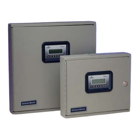
IEE 03858-06-0205 User manual

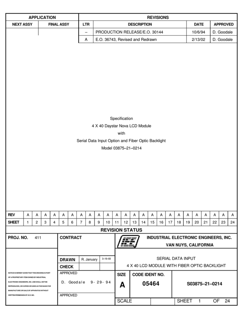
APPLICATION REVISIONS
NEXT ASSY FINAL ASSY LTR DESCRIPTION DATE APPROVED
–PRODUCTION RELEASE/E.O. 29204 3/9/93 D. Goodale
AE.O. 29436 6/3/93 D. Goodale
BE.O. 29541 6/28/93 D. Goodale
CE.O. 36743, Revised and Redrawn 2/13/02 D. Goodale
Specification
4 X 20 Daystar Nova LCD Module
with
Serial Data Input Option and EL Backlight
Model 03858–06–0205
REV C C
SHEET 25 26 27 28 29 30 31 32 33 34 35 36 37 38 39 40 41 42 43 44 45 46 47 48
REV CCCCCCCCCCCCCCCCCCCCCCCC
SHEET 1 2 3 4 5 6 7 8 9 10 11 12 13 14 15 16 17 18 19 20 21 22 23 24
REVISION STATUS
PROJ. NO. 411 CONTRACT INDUSTRIAL ELECTRONIC ENGINEERS, INC.
VAN NUYS, CALIFORNIA
DRAWN R. January 3–19–93 SERIAL DATA INPUT
CHECK 4 X 20 LCD MODULE WITH EL BACKLIGHT
NOTICE IS HEREBY GIVEN THAT THIS DRAWING IS PART
OF A PROPRIETARY ITEM OWNED BY INDUSTRIAL
APPROVED SIZE CODE IDENT NO.
ELECTRONIC ENGINEERS, INC. AND SHALL NOT BE
REPRODUCED, OR COPIED OR USED AS THE BASIS FOR
MANUFACTURE OR SALE OF APPARATUS WITHOUT
D. Goodale 3-9-93 A05464 S03858–06–0205
WRITTEN PERMISSION OF I.E.E. INC. APPROVED SCALE SHEET 1OF 26

Table of Contents
Paragraph Title Page
Industrial Electronic Engineers, Inc. SIZE
ACODE IDENT NO.
05464 S03858–06–0205
Van Nuys, California SCALE N/A REV C SHEET 2
1.0 GENERAL INFORMATION...............................................................................................................5
1.1 Introduction.......................................................................................................................................5
1.2 Application........................................................................................................................................5
1.3 Standard Features ...........................................................................................................................5
1.4 Description.......................................................................................................................................5
2.0 LOGICAL STRUCTURE AND FUNCTION......................................................................................6
2.1 LCD Module......................................................................................................................................6
2.1.1 Signal Description............................................................................................................................6
2.2 LCD Controller.................................................................................................................................7
2.2.1 Instruction Register (IR)..................................................................................................................7
2.2.2 Data Register (DR)..........................................................................................................................7
2.2.3 Busy Flag.........................................................................................................................................7
2.2.4 Address Counter (AC)......................................................................................................................7
2.2.5 Display Data RAM (DD RAM) ..........................................................................................................8
2.2.6 Character Generator ROM (CG ROM)............................................................................................8
2.2.7 Character Generator RAM (CG RAM)..............................................................................................9
2.2.8 Parallel/Serial Data Conversion Circuitry, Timing Generator Circuitry............................................9
3.0 THEORY OF OPERATION..............................................................................................................9
3.1 Serial Interface.................................................................................................................................9
3.2 Error Detection and Reporting.........................................................................................................9
3.3 Power–up Sequence........................................................................................................................9
3.4 Transmission Sequence for Instructions.........................................................................................9
3.5 Instruction Set..................................................................................................................................9
3.5.1 Instruction Summary........................................................................................................................9
3.5.2 Sample Instructions In BASIC..........................................................................................................9
3.6 Down–Loadable Special Characters...............................................................................................9
3.7 Self–test...........................................................................................................................................9
3.8 Diagnostics......................................................................................................................................9
4.0 INTERFACE AND CONTROL.........................................................................................................9
4.1 Connector Assignment (P2)............................................................................................................9
4.2 Jumper Settings...............................................................................................................................9
5.0 ELECTRICAL SPECIFICATIONS....................................................................................................9
5.1 Absolute Maximum Ratings .............................................................................................................9
5.2 Normal Operating Ratings ...............................................................................................................9
5.2.1 Power–up Supply Requirements.....................................................................................................9
5.2.2 External Reset Requirements..........................................................................................................9
5.3 Interface Signals...............................................................................................................................9
5.3.1 Serial Interface Signals ....................................................................................................................9
6.0 ENVIRONMENTAL CHARACTERISTICS........................................................................................9
6.1 Operating..........................................................................................................................................9

Table of Contents
Paragraph Title Page
Industrial Electronic Engineers, Inc. SIZE
ACODE IDENT NO.
05464 S03858–06–0205
Van Nuys, California SCALE N/A REV C SHEET 3
6.2 Non–Operating................................................................................................................................9
7.0 OPTICAL SPECIFICATIONS...........................................................................................................9
7.1 Optical Characteristics....................................................................................................................9
7.2 Viewing Angle Adjustment...............................................................................................................9
8.0 EL BACKLIGHTING..........................................................................................................................9
8.1 EL Backlight Description..................................................................................................................9
8.2 Electrical Characteristics of EL Backlight........................................................................................9
8.3 Operation..........................................................................................................................................9
8.3.1 Normal Operation.............................................................................................................................9
8.3.2 Brightness, Voltage and Frequency Characteristics.......................................................................9
8.3.3 Intermittent Operation.......................................................................................................................9
8.3.4 Square Waveform Operation...........................................................................................................9
8.3.5 Operating Temperature....................................................................................................................9
8.3.6 Operating Life..........................................................................................................................................9
8.4 Electromagnetic Interference (EMI) .................................................................................................9
8.5 DC–AC Inverter................................................................................................................................9
9.0 INSTALLATION NOTE.....................................................................................................................9
10.0 ACCESSORIES...............................................................................................................................9
11.0 OUTLINE AND INSTALLATION CHARACTERISTICS....................................................................9

List of Figures
Figure Title Page
Industrial Electronic Engineers, Inc. SIZE
ACODE IDENT NO.
05464 S03858–06–0205
Van Nuys, California SCALE N/A REV C SHEET 4
Figure 1 Module Block Diagram.....................................................................................................................6
Figure 2 LCD Controller Block Diagram ........................................................................................................7
Figure 3 Correspondence Between Character Codes and Character Patterns...........................................8
Figure 4 Relationship Between CG RAM Address, Character Codes (DD RAM) and Character Patterns
(CG RAM Data)................................................................................................................................9
Figure 5 8–bit Serial Data Format..................................................................................................................9
Figure 6 Default Configuration at Power–up..................................................................................................9
Figure 7 Instruction Sequence.......................................................................................................................9
Figure 8 Data Sequence................................................................................................................................9
Figure 9 Instruction Set..................................................................................................................................9
Figure 10 Down–loadable Special Characters................................................................................................9
Figure 11 Power Supply Requirements...........................................................................................................9
Figure 12 External Reset Circuit......................................................................................................................9
Figure 13 Definition of Vertical Viewing Angle..................................................................................................9
Figure 14 Definition of Horizontal Viewing Angle..............................................................................................9
Figure 15 Definition of Contrast Ratio (CR).....................................................................................................9
Figure 16 Definition of Optical Response........................................................................................................9
Figure 17 Initial Brightness vs. Voltage............................................................................................................9
Figure 18 Initial Brightness vs. Frequency.......................................................................................................9
Figure 19 Brightness vs. Time.........................................................................................................................9
Figure 20 03858–06–0205 Outline Drawing.....................................................................................................9

Industrial Electronic Engineers, Inc. SIZE
ACODE IDENT NO.
05464 S03858–06–0205
Van Nuys, California SCALE N/A REV C SHEET 5
1.0 GENERAL INFORMATION
1.1 Introduction
This specification describes the serial interface Daystar Nova model 03858–06–0205, a 4–line supertwisted
liquid crystal display (LCD) with 20 characters per line.
Model Number Designation System
03858 – 06 – 0 2 0 5
Transflective STN
LCD w/EL Backlight 4x20 Format Reserved 1 = Parallel Data Input *
2 = Serial Data Input 0 = External
Backlight Power 0 = Aviation
Green Color
* Parallel standard, Serial optional
1.2 Application
Daystar Nova modules provide alphanumeric information which is easily readable in high ambient light or in
darkness with backlight activated. The low power requirements of the modules make them suitable for portable
battery operated equipment. The wide operating temperature range (–30° to +80°C) is ideal for most outdoor
applications. The choice of a preferential viewing hemisphere is not necessary because of the excellent wide
angle viewing characteristics of the new Super Bi–refringent Effect (SBE) liquid crystal cell used in this display.
The serial data input model of the 03858–06 Daystar Nova display allows communication between a host
processor and the display by means of a serial RS–232C interface. This provides the capability to
communicate over a longer distance than is possible with the parallel model. The RS–232 interface is a two
wire communication link.
1.3 Standard Features
•Serial data communication via RS–232C
•Multiple baud rates: 1200, 2400, 4800, and 9600
•Low power consumption
•Wide temperature range
•Built–in diagnostics
•Down–loadable special characters
1.4 Description
The serial input Daystar Nova module includes an on–board CMOS microprocessor which translates serial
data into parallel data and provides other enhancements over the parallel model. The serial data may be set by
a jumper to accommodate speeds of 1200, 2400, 4800, and 9600 baud. Parity may also be set by jumper for
odd, even, or no parity. The electrical interface is RS–232C compatible.
A single +5 Volt nominal power supply is required for operation. The unit operates from 4.50 Volts to 5.50 Volts.
The typical power requirement for the module is 120mW.
The module weighs 9.1 ounces (257.7 grams).

Industrial Electronic Engineers, Inc. SIZE
ACODE IDENT NO.
05464 S03858–06–0205
Van Nuys, California SCALE N/A REV C SHEET 6
2.0 LOGICAL STRUCTURE AND FUNCTION
2.1 LCD Module
Figure 1 illustrates the major components of the serial option Daystar Nova module. The module provides
means for an external viewing angle adjustment potentiometer (VBIAS Adj.) at Pin 4, and connections for optional
RESET and self–test switches at Pins 3 and 5. The external viewing angle adjustment potentiometer should be
connected to the same +5 Volt supply as the display module. RESET and TEST pull down to ground to
activate the function. All three inputs may be left open if not used. The VBIAS test point is used at the factory to
preset the viewing angle.
Column Drivers
Column DriversMicroprocessor
Temperature
Compensation
3
5
8
7
6
4
1
2
10
11
TPVBIAS
VBIASAdj
Reset
Test
GND
+5V
R
X
RXRtn
–
+
Serial
Receiver
+5V
View Angle
Adjust
Backlight
Option
LCD
Cell
LCD
Controller
EL Backlight
6” Flying Leads
Figure 1Module Block Diagram
2.1.1 Signal Description
Signal Name Number Of Lines Input/Output Connected
RESET 1IMPU
TEST 1IMPU
VBIAS TP 1OTemp. Comp. Ckt.
VBIAS Adj. 1ITemp. Comp. Ckt.
RX 1ISerial Receiver
RX Rtn 1ISerial Receiver
VCC 2 – Power
GND 7 – –

Industrial Electronic Engineers, Inc. SIZE
ACODE IDENT NO.
05464 S03858–06–0205
Van Nuys, California SCALE N/A REV C SHEET 7
2.2 LCD Controller
The LCD Controller includes all of the circuitry necessary to take parallel input data and create the necessary
control functions and characters. The block diagram of the controller is shown in Figure 2 below. The
remaining subparagraphs of Section 2 describe the major function blocks.
DB4–DB7
E
R/W
RS
DB0–DB3
4
4
I/O Buffer
Instruction
Decoder
Instruction
Register (IR) Data
Register (DR)
Busy
Flag
I/O Buffer
8
Character
Generator
RAM
(CG RAM)
512 Bits
Cursor Blink
Control Circuit
Display Data
RAM
(DD RAM)
80x8 bits
8
88
Character
Generator
ROM
(CG ROM)
7200 Bits
8
7
7
Timing Generation
Circuit
Address
Counter (AC)
7
Common Signal
Driver
16–bit Shift
Register
3
16 16
CL1
CL2
M
Parallel/Serial Data
Conversion Circuit
(Parallel Data –Serial Data)
40–bit Latch
Circuit
Segment Signal
Driver
40–bit Shift Register
Seg1–Seg40
Com1–Com16
D
5 5
40
Figure 2LCD Controller Block Diagram
2.2.1 Instruction Register (IR)
The IR stores instruction codes such as display clear and cursor shift, and address information of the display
data RAM (DD RAM) and character generator RAM (CG RAM). The IR can be written from the MPU, but not
read.
2.2.2 Data Register (DR)
The DR temporarily stores data to be written into or read from the DD RAM or the CG RAM.
2.2.3 Busy Flag
When the Busy Flag is a "1", the module is in an internal operating mode and ignores any additional instructions
(Refer to Read Busy Flag and Address instruction).
2.2.4 Address Counter (AC)
The AC determines the address of the DD RAM or CG RAM in which new data is stored. After writing into (or
reading from) the DD RAM or CG RAM, the AC is incremented or decremented as defined by the

Industrial Electronic Engineers, Inc. SIZE
ACODE IDENT NO.
05464 S03858–06–0205
Van Nuys, California SCALE N/A REV C SHEET 8
Increment/Decrement bit (Refer to Entry Mode Set instruction).
2.2.5 Display Data RAM (DD RAM)
The DD RAM contains 80 X 8 bits and represents 80 characters. The relationship between the DD RAM
address and position of the characters in the display can be controlled by the user (Refer to Entry Mode Set and
Cursor or Display Shift instructions).
2.2.6 Character Generator ROM (CG ROM)
The CG ROM generates character patterns of 5 X 7 dots from 8 bit character codes. The 192 5 X 7 dot matrix
characters are illustrated in Figure 3.
Figure 3Correspondence Between Character Codes and Character Patterns
Note:Addresses 00h through 0Fh are reserved for CG RAM Addressing. Addresses 10h through 1Fh and
80h through 9Fh are not used.

Industrial Electronic Engineers, Inc. SIZE
ACODE IDENT NO.
05464 S03858–06–0205
Van Nuys, California SCALE N/A REV C SHEET 9
2.2.7 Character Generator RAM (CG RAM)
The CG RAM allows the user to define 8 types of 5 X 7 character patterns. Figure 4 shows the relationship
between CG RAM addresses and data patterns (Refer to Set CG RAM Address and Write to CG or DD RAM
instructions).
Character Codes
(DD RAM Data) CG RAM
Address Character Patterns
(CG RAM Data)
76543210 543210 76543210
←Higher Order Bits
Lower Order Bits→←Higher Order Bits
Lower Order Bits→←Higher Order Bits
Lower Order Bits→
000 ***11110
001 10001
010 10001Character
011 11110Pattern
0000*000 000100 10100Example
101 10010
110 10001
111 ***00000←Cursor
Figure 4Relationship Between CG RAM Address, Character Codes (DD RAM)
and Character Patterns (CG RAM Data)
NOTES:
1) The CG RAM consists of 64 bytes. Any bytes not used for character pattern information can be
used for general purpose data RAM. The 5, 6 and 7 bits are never used for character pattern
information and are always available for use.
2) The 0, 1 and 2 bits of character code correspond to the 3, 4 and 5 bits of the CG RAM address.
3) The 0, 1 and 2 bits of the CG RAM address specify the row of the character pattern.
4) The 8th row of the character pattern corresponds to the cursor character pattern. If any bit in the
row is "1", then the corresponding cursor bit is a "1" regardless of cursor position. (For most
applications, the data should be "0" in this row, which allows for normal cursor operation on the
character.)
5) Since bit 3 is a "don't care", two character codes represent the same special character. For
example, a character code of 07 (hexadecimal) selects the same character pattern as OF
(hexadecimal).
2.2.8 Parallel/Serial Data Conversion Circuitry, Timing Generator Circuitry
These blocks control the interface to the LCD drivers.

Industrial Electronic Engineers, Inc. SIZE
ACODE IDENT NO.
05464 S03858–06–0205
Van Nuys, California SCALE N/A REV C SHEET 10
3.0 THEORY OF OPERAT ION
The serial input option was designed to allow users to send data and control codes to the display module via
the industry standard RS–232C serial interface. This follows the interface protocol of the parallel input Daystar
Nova display modules with few exceptions.
3.1 Serial Interface
The serial input module is a receive only device. Consequently, it is impossible for the host to read data or
status from the LCD controller. This precludes reading of data from the Data Display (DD) RAM, Character
Generator (CG) RAM, or address counter (AC). It is not necessary to read the controller busy flag because a
large serial data input buffer prevents overflow at 9600 baud.
The serial interface requires one start bit, and may be jumper selected to operate with (1) either 7 or 8 data bits
per character and (2) either odd or even parity with one stop bit, or no parity and two stop bits.
Since two command characters and numerous data characters are 8 bits in length, it is recommended to
operate in 8 bit mode if the host has this capability. Where this is not possible, 7 bit mode should be jumper
selected (see section 4.2) and a special command character (19h) must be sent prior to each 8 bit command
or data character; i.e., characters where B7= 1.
Figure 5 represents serial data formatted as one start bit, eight data bits, an odd or even parity with one stop bit,
or 2 stop bits if no parity.
Mark
Space B B B B B B B P SB
210 3 4 5 6 7
(LSB) (MSB)
Start Bit 8 Data Bits
Figure 58–bit Serial Data Format
A logic "1" represents a "mark" condition and a logic "0" represents a "space" condition. For RS–232C the
"mark" and "space" conditions are defined as –3.0 to –25.0 Volts and +3.0 to +25.0 Volts, respectively.
3.2 Error Detection and Reporting
During normal operation, the module will detect and display all parity and framing errors (see Section 3.8).
Each character received in error is replaced with one of the following symbols:
Parity Error "&"
Framing Error "@"
If the display shows an "@" after power–up, the polarity of the serial interface may be reversed and should be
checked.

Industrial Electronic Engineers, Inc. SIZE
ACODE IDENT NO.
05464 S03858–06–0205
Van Nuys, California SCALE N/A REV C SHEET 11
3.3 Power–up Sequence
Upon power–up, the serial Daystar Nova display module is automatically initialized to the format defined by the
jumper settings and default values shown in Figure 6. The power–up sequence takes about 0.5 second.
Baud rate: Jumper defined (per section 4.2)
Parity bit present: "
Parity checking enable: "
Parity (Odd or Even): "
7 or 8 data bits "
Multiplex rate of LCD: "
Display clear: YES
Display ON/OFF: ON
Cursor location: Position 0
Cursor: OFF
Entry mode set: Shift cursor right after character entry
Controller: 1
Data/Instructions: Data
Figure 6Default Configuration at Power–up
3.4 Transmission Sequence for Instructions
Figures 7 and 8 depict the recommended sequence for each data or instruction transmission.
11h
Byte 1 2 3 4 n
Figure 7Instruction Sequence
Byte 1 2 3 4 n
12h
Figure 8Data Sequence

Industrial Electronic Engineers, Inc. SIZE
ACODE IDENT NO.
05464 S03858–06–0205
Van Nuys, California SCALE N/A REV C SHEET 12
3.5 Instruction Set
Instruction Code Description Execution
DB7DB6DB5DB4DB3DB2DB1DB0Time (Max)
Clear Display 00000001Clears entire display and sets DD RAM to 0 1.64 ms
Return Home 0000001*
Sets DD RAN counter to 0. If the display has been
shifted, characters are returned to their initial
positions. DD RAM contents remain unchanged. 1.64 ms
Entry Mode Set 000001I/D SSets shift register direction and cursor movement
direction which occur during data read and write
operations
40µs
Display ON/OFF
Control 00001DCBTurns ON/OFF the entire display (D), cursor) and
cursor blink attribute (B). 40µs
Cursor or Display
Shift 0 0 0 1 S/C R/L * * Moves cursor or shifts entire display one position.
DD RAM contents are unchanged. 40µs
Function Set 001DL 1 0 * * Sets Interface Data Length. 40µs
Set CG RAM
Address 0 1 Sets CG RAM address. CG RAM data is sent or
received after this is set. 40µs
Set DD RAM
Address 1Sets DD RAM address. DD RAM data is sent or
received after this is set. 40µs
Read Busy Flag
and Address BF Reads Busy Flag (BF) and Address Counter 0µs
Write Data to CG
or DD RAM Writes data into CG RAM or DD RAM. 40µs
Read Data from
CG or DD RAM Reads data from CG RAM or DD RAM. 40µs
Controller 1
Instructions 00010001Subsequent data is Display Module Instructions for
controller 1.
Controller 1
Data 00010010Subsequent data is Display Module data for
controller 1.
Controller 2
Data 00010110Subsequent data is Display Module data for
controller 2.
Controller 2
Instructions 00010101Subsequent data is Display Module Instructions for
controller 2.
8 Bit Data
Instructions 00011001Causes microprocessor to add B7=1 to the next
character received.
Down Load
Special Character 00010111Subsequent 2 characters define ROM address of
characters, and its down load DD Ram address
I/D=1: Increment DD RAM: Display Data RAM
I/D=0: Decrement CG RAM: Character Generator RAM
S=1: Enable Shift Operation ACG CG RAM Address
S/C=1: Shift Display ADD DD RAM Address
S/C=0: Shift Cursor (Corresponds to cursor
address)
R/L=1: Shift Right AC Address Counter
R/L=0: Shift Left (used for both CG and DD RAM)
DL=1: 8–bit operation *Don’t Care

Industrial Electronic Engineers, Inc. SIZE
ACODE IDENT NO.
05464 S03858–06–0205
Van Nuys, California SCALE N/A REV C SHEET 13
DL=0: 4–bit operation
BF=1: Operating internally
BF=0: Can accept instruction
Figure 9Instruction Set

Industrial Electronic Engineers, Inc. SIZE
ACODE IDENT NO.
05464 S03858–06–0205
Van Nuys, California SCALE N/A REV C SHEET 14
3.5.1 Instruction Summary
Hex Code Command
01h Clear Display
02h Home Cursor
04h Disable Shift And Decrement
05h Enable Shift And Decrement
06h Disable Shift And Increment
07h Enable Shift And Increment
08h Turn Display Off
0Ch Turn Display On And Cursor Off
0Eh Turn Display On And Cursor On
0Fh Turn Display On And Blink Cursor
10h Shift Cursor To The Left
14h Shift Cursor To The Right
18h Shift Display To The Left
1Ch Shift Display To The Right
11h Subsequent Data Is Controller 1 Instruction(S)
12h Subsequent Data Is Controller 1 Display Data
15h Subsequent Data Is Controller 2 Instruction(S)
16h Subsequent Data Is Controller 2 Display Data
17h Subsequent Data Down Loads Special Characters
19h Subsequent Data Is 8 Bit Length Character
3.5.2 Sample Instructions In BASIC
The following instructions are provided as an example to illustrate the correct form and to assist the user to
rapidly see his display operate.
10 CLOSE #1 ‘Close if open
20 OPEN "COM1:9600,N,8,2,CS,DS" AS #1 'Setup serial port
30 PRINT #1, CHR$(&H4A); CHR$(&H61); CHR$(&H6E) 'Display date
40 PRINT #1, CHR$(&H2D); CHR$(&H32); CHR$(&H2D)
50 PRINT #1, CHR$(&H39); CHR$(&H36)
60 PRINT #1, CHR$(&H11); CHR$(&H0F) 'Blink cursor
70 PRINT #1, CHR$(&H84) 'Move cursor to day
80 PRINT #1, CHR$(&H12) 'Prepare to change day
90 SYSTEM
The display should appear as follows:
Jan–2–96

Industrial Electronic Engineers, Inc. SIZE
ACODE IDENT NO.
05464 S03858–06–0205
Van Nuys, California SCALE N/A REV C SHEET 15
3.6 Down–Loadable Special Characters
An added feature of the serial input module is the inclusion of a group of 206 special characters stored in its
memory. These supplement the character library of the LCD module and may be easily down loaded (up to
eight at a time) into the CG RAM of the display module for use in one display frame of the display. Thus, in
addition to being able to input his own character designs as described in Paragraph 2.2.7, the user has these
additional preformatted characters available. Note that all down loaded character data is lost and must be
reloaded after power has been removed.
To facilitate the use of these characters, a "subsequent data" instruction (17h) is used to inform the
microprocessor that the following two bytes of data identify (1) the location of the special character to be down
loaded, and (2) the CG RAM location where it is to be loaded. This instruction sequence is as follows.
17h
(1)
Character
Locations
00h – E5h
(2)
CG RAM
Locations
00h – 07h
Figure 10 defines the format of these special characters and their memory location used to select them. The
eight CG RAM locations to which they may be sent are from 00h to 07h.

Industrial Electronic Engineers, Inc. SIZE
ACODE IDENT NO.
05464 S03858–06–0205
Van Nuys, California SCALE N/A REV C SHEET 16
Figure 10 Down–loadable Special Characters

Industrial Electronic Engineers, Inc. SIZE
ACODE IDENT NO.
05464 S03858–06–0205
Van Nuys, California SCALE N/A REV C SHEET 17
3.7 Self–test
The serial input display module can be operated independently from the host by using the "Self–test" option.
1. Check the multiplex jumper for proper setting (Section 4.2).
2. Connect a +5V power supply and potentiometer as discussed in Paragraph 2.1 and Figure 1.
3. Momentarily short the self–test line to GND (P2 pin 5 to pin 8).
4. All character positions should display the character "H".
5. The module can be stepped through the remaining test display frames by using the self–test line as
in Step 3 (above). The display will advance from frame to frame each time the self–test line is
momentarily shorted to ground. The remaining frames display: I, #, all pixels on, jumper settings in
HEX (with jumper #8 being the LSB, see Section 4.2), firmware version number, and then
resumption of normal operation.
6. Upon completion of "Self–test", the module is returned to the normal mode of operation with its
previous controller and data/instruction (RS bit) settings.
3.8 Diagnostics
1. The display module can be operated by the host in a HEX dump mode. This diagnostic mode
provides for the HEX display of all serial data received. While operating in this mode, the module will
ignore the multiplex jumper setting and operate the display in a 1/8 multiplex mode.
2. Check the module jumpers for proper baud speed and parity settings (Section 4.2).
3. With power "OFF" short the self–test line to GND (P2 pin 5 to pin 8).
4. While the self–test line is shorted to ground, apply +5 Volts to the display module. The self–test line
is now ineffective and may be allowed to float.
5. All serial data received will now be displayed in HEX. To return to the normal operating mode,
remove power, allow the self–test line to float, and re–apply power.
If a parity or framing error should occur, the most significant nibble of the HEX code will be displayed as:
HEX Code Parity Error Framing Error
0X GX gX
1X HX hX
2X IX iX
3X JX jX
4X KX kX
5X LX lX
6X MX mX
7X NX nX
8X OX oX
9X PX pX
AX QX qX
BX RX rX
CX SX sX
DX TX tX
EX UX uX
FX VX vX
X = Least significant nibble
* Characters with parity and framing errors are displayed as framing errors only. Framing errors can occur
due to loss of serial bit timing, improper baud rate and/or parity setting.

Industrial Electronic Engineers, Inc. SIZE
ACODE IDENT NO.
05464 S03858–06–0205
Van Nuys, California SCALE N/A REV C SHEET 18
4.0 INTERFACE AND CONTROL
4.1 Connector Assignment (P2)
Pin No. Function
P2–1 RXData
P2–2 RXData RTN (Signal Ground)
P2–3 RESET
P2–4 Adjust
P2–5 Self–Test
P2–6 VBIAS (Factory Test Point)
P2–7 VCC (+5 Volts)
P2–8 VSS (Ground)
P2–9 No Connection
P2–10 Optional Backlight
P2–11 Optional Backlight
4.2 Jumper Settings
Jumper No. Pins Jumper A = “0” Jumper B = “1”
1E1 4800 Baud 1200 Baud
2E2 2 x Baud 1 x Baud
3E3 Parity No Parity♦
4E4 Even Parity Odd Parity
5E5 7 Data Bits *** 8 Data Bits
6E6 1/8 Mpx (N/A) 1/16 Mpx
7** Not Used
8** Not Used
*Baud rate will default to "1" if no jumper is installed.
** Jumper options 7, and 8 are omitted and will indicate as logic "1" when in self–test mode.
*** 8 bit word preferred. When 7 bit word is selected see section 3.1.2 for use of instruction 19 Hex.
♦Selection of NO PARITY requires use of two stop bits.
NOTE: The mating connector
must be wired in a reverse pin
sequence from its marking. (Pin
11 is Pin 1 etc.)
The mating connector is a Molex
#22-01-2117 or equivalent. It uses
crimp pins #08-50-0114.

Industrial Electronic Engineers, Inc. SIZE
ACODE IDENT NO.
05464 S03858–06–0205
Van Nuys, California SCALE N/A REV C SHEET 19
5.0 ELECTRICAL SPECIFICATIONS
5.1 Absolute Maximum Ratings
Power Supply Voltage (VCC): –0.3 to +6.5 VDC
Serial Input Voltage: –25.0 to +25.0 VDC
5.2 Normal Operating Ratings
Power Supply Voltage (VCC): +5.0 VDC ±10%
Supply Current (+5 VDC): 34 mA Max
EL Current (+5 Volt Inverter) 100 mA
5.2.1 Power–up Supply Requirements
Initialization may or may not be performed completely unless the rise time (tRCC) of the power supply is correct
at turn–on (1ms <tRCC <10ms). Figure 11 represents the requirements of the power supply. Note that tOFF
stipulates the minimum time that power can be OFF (tOFF >1ms) during a momentary dip or when the power
supply cycles ON and OFF.
0.2V
4.5V
tRCC tOFF
VCC
Figure 11 Power Supply Requirements
5.2.2 External Reset Requirements
To utilize the optional external reset, the RESET pin must be held at ground (<0.5 Volts) for at least 10
milliseconds after the power supply is within the voltage tolerance. Figure 12 shows the module Reset circuit.
+5V
1k
3.3k
330
1uF
Microprocessor
Internal
Pull–down
J2–Pin 3
Figure 12 External Reset Circuit

Industrial Electronic Engineers, Inc. SIZE
ACODE IDENT NO.
05464 S03858–06–0205
Van Nuys, California SCALE N/A REV C SHEET 20
5.3 Interface Signals
5.3.1 Serial Interface Signals
The display is designed to be operated by a standard RS–232 serial interface. The user can operate the
module with any interface which meets the following requirements for a "mark" condition and a "space"
condition. The user should observe generally accepted design rules when interfacing to the display.
Space Voltage
(VRX Data – VRX Data RTN) +3.0 to +25.0 Volts
Mark Voltage
(VRX Data – VRX Data RTN) –25.0 to +0.8 Volts
6.0 ENVIRONMENTAL CHARACTERISTICS
6.1 Operating
Temperature: –30 to +80°C (Backlight Off)
–30 to +40ºC (Backlight On, See Paragraph 8.3.5)
Humidity: (@ 40ºC) 95% RH (non–condensing)
Humidity (<40°C): Absolute humidity must be lower the humidity of 95% RH at 40°C
Vibration: 10g at 10 to 400Hz (3 axes)
Shock: 10g (all axes)
6.2 Non–Operating
Temperature: –40°C to +85°C
This manual suits for next models
1
Table of contents
Other IEE Monitor manuals
IEE
IEE SL330-X41H User manual
IEE
IEE PDK 404A-0WG13L User manual
IEE
IEE PDK UP03-0BG03L User manual
IEE
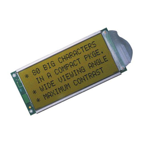
IEE 03858-06-0105 User manual
IEE
IEE PDK 111C-0WG13L User manual
IEE
IEE PDK 4005-0WG13L User manual
IEE
IEE PDK 4003-0WG13L User manual
IEE
IEE PDK 0212-OWG13L User manual
IEE
IEE PDK 102B-CWG03L User manual
IEE
IEE 03858-21-0205 User manual
IEE
IEE PDK 0013-CBG13L User manual
IEE
IEE PDK 4UP3-0BG03L User manual
IEE
IEE 03875-06-0114 User manual
IEE
IEE 03875-06-0214 User manual
IEE
IEE PDK 004A-OWG13L User manual
IEE
IEE PDK 111B-CBB13M User manual

IEE
IEE PDK 4U03-0BG13L User manual
IEE
IEE PDK 225U-0WG13L User manual
IEE
IEE 03875-21-0114 User manual
IEE
IEE 03601-95B-40 User manual
