IOTA APIS FUZZ User manual

— APIS FUZZ (2021-06-30)
APIS FUZZ
Inspired by the TMR Bumble Buzz.
All trademarks and registered trademarks are the property of their respective owners.!The company and product names used
in this document are for identification purposes only. Use of these names and brands does not imply endorsement.

— APIS FUZZ (2021-06-30)
SUMMARY
The APIS FUZZ is inspired by the TMR Bumble Buzz, a knob-less octave-up fuzz using a
phase splitter followed by a differential pair to emphasise the upper octave.
It features an optical true bypass, allowing for a smaller DPDT footswitch with a click
more subtle than with a common 3PDT footswitch.
APIS FUZZ LINEAGE
The Superfuzz was originally developed by Shin-ei in Japan in the late 1960s, and re-
packaged for various brands, including Univox.
The F-1 Fuzz Tone is essentially a low-cost version of the Superfuzz. It’s one of Kay's
budget effects from the 60s, housed in a plastic treadle pedal. It has a simpler front, no
variable drive, no output level control and no gain recovery stage after the mid scoop.
The Bumble Buzz removes the last pot from the circuit, replacing it with a fixed and
slightly modified tone stack.
No direct support is offered beyond the documentation provided here.
This document is written assuming some experience building pedals. Replacement parts
are only offered for missing or defective components.
DIFFICULTY
EASY
POWER
5 mA at 9 V DC
IMPEDANCE
Zin = 30 kΩat 1 kHz
Zout = 33 kΩat 1 kHz

— APIS FUZZ (2021-06-30)
PARTS LIST
RESISTORS
1x 1k5
2x 1k8
6x 10k
1x 22k
1x 42k
1x 47k
4x 100k
1x 330k
1x 1M
CAPACITORS
FILM
1x 1n (WIMA: 1000)
1x 2n2 (WIMA: 2200)
1x 22n (WIMA: 0,022)
2x 100n (WIMA: 0,1)
MLCC
1x 220n
ELECTROLYTIC
2x 1u
1x 2u2
3x 10u
1x 100u
DIODES
1x 3mm LED
1x 1N5817
4x 1N4007
TRANSISTORS
4x 2N2222
PHOTOFETS
1x TLP222G
HARDWARE
1x Hammond 1590A enclosure
1x Alpha DPDT footswitch, latching
2x Lumberg 1/4” jack, mono
1x Lumberg DC jack, 2.1 mm
1x 3mm LED bezel
OTHER
APIS FUZZ PCB
Wires

— APIS FUZZ (2021-06-30)
BUILD STEPS
1. SOLDER PASSIVE COMPONENTS
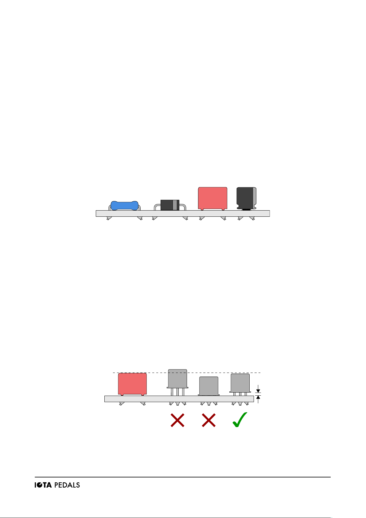
Solder all components onto the PCB, starting with the lowest-profile ones, i.e. resistors
and diodes — excluding the LED. The painted bands on the diodes need to line up with
the bands on the PCB.
Continue with the capacitors. It’s important that they sit flush on the board, there isn’t
much clearance in the 1590A enclosure.
Electrolytic capacitors are polarised, which means they have a specific orientation.
Make sure that the negative terminal of the capacitor is in the correct pad. Film and
ceramic capacitors have no polarisation and can be installed in any orientation.
2. SOLDER ACTIVE COMPONENTS
Solder the transistors and the photofet. These components are very sensitive, apply heat
only for a very short time. Consider letting them cool down after each lead is soldered.
These devices are also sensitive to electrostatic discharge (ESD), take care.
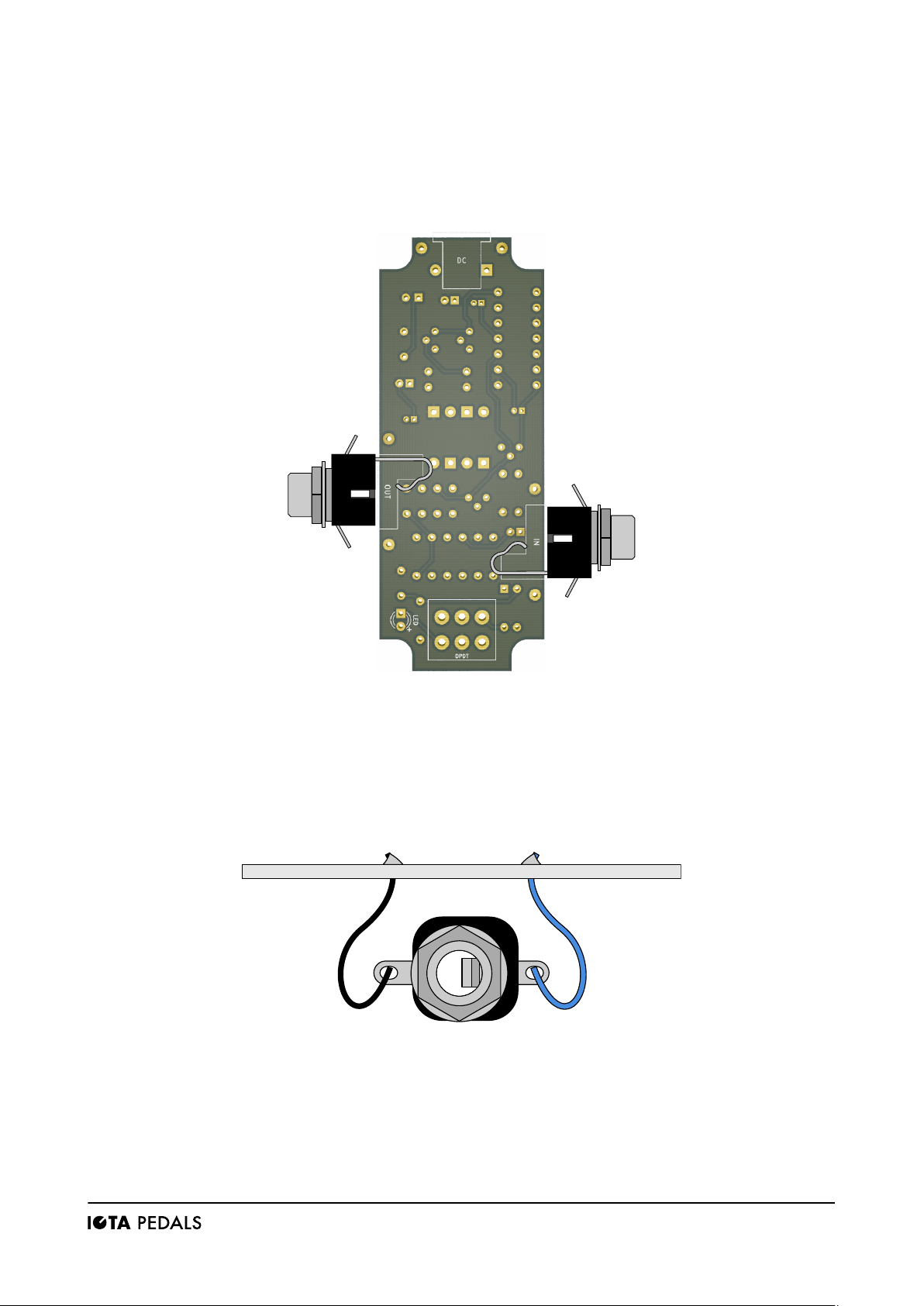
Make sure the TLP222G photofet is properly oriented. The point on the photofet must be
aligned with the point of its footprint on the PCB.
Push the 2N2222 metal can transistors down firmly, but gently. They must not touch the
PCB and should not be taller than the film capacitors.

— APIS FUZZ (2021-06-30)
3. WIRE UP AUDIO JACKS
The input jack must have the signal solder lug pointing towards the footswitch. The
output jack’s signal solder lug must point in the opposite direction. If unsure, check the
bottom side of the PCB for the orientation of the jacks.
Measure four wires of at least 3.5 cm length and strip off about five millimetres of
insulation at each end. The wires should be as short as possible, yet long enough to
leave some slack to make it easy to put the PCB into the enclosure.

— APIS FUZZ (2021-06-30)
4. MOUNT THE FOOTSWITCH
Insert the footswitch and fasten it lightly. Make sure the bottom nut is as close to the
footswitch body as possible, otherwise the PCB will not sit low enough in the enclosure.
5. WIRE UP THE DC JACK
Measure two wires of about 3.5 cm length and strip off about five millimetres of
insulation at each end.
Solder them to the DC jack and mount the DC jack inside the enclosure, threading the
two wires through the nut. Check the PCB for the orientation of the +9V and GND pads.
Tighten the nut of the DC jack and solder the two wires to the PCB. The longer lug of the
DC jack must connect to the +9V pad.
!
•Top Nut
•Flat Shim Washer
(Enclosure)
•Split Lock Washer
•Bottom Nut

— APIS FUZZ (2021-06-30)
6. PUT THE PCB INTO THE ENCLOSURE
Take the nuts and washers off the audio jacks and put the PCB into the enclosure. Before
fastening the jacks make sure they are sideways (see section 3) so the board sits as low
as possible in the enclosure.
Tighten the footswitch nut. Don’t solder it just yet.
7. MOUNT THE LED
Push the LED through the bezel, until it snaps in place.
From the outside, insert the LED and bezel through the small hole next to the footswitch
and the LED's legs through the two pads in the PCB. The longer, positive leg goes to the
solder pad marked with a + sign.
8. SOLDER THE FOOTSWITCH AND LED
When all components are fastened and set in place, solder the LED and the footswitch.
Make sure the PCB sits low enough so that no component is higher than the edge of the
enclosure. It’s supposed to be a tight fit but there’s a 1-2 mm tolerance.
CONGRATULATIONS!
Give your new pedal a test drive. If everything works as expected, screw on the lid and
you’re done.

— APIS FUZZ (2021-06-30)

— APIS FUZZ (2021-06-30)
OPTIONAL: REPLACING THE LED
The red low-current LED (D2) is part of the optical true bypass.
Replacing it for one with a different brightness or colour might require adjusting the
value of the current-limiting resistor R1 (CLR).
The TLP222G photofet (U1) has a maximum trigger LED current of IFT = 3 mA and a
maximum forward voltage of Vf= 1.3 V. Any replacement LED thus must be driven by at
least 3 mA.
DETERMINING THE NEW RCLR
Measure the forward voltage VLED of the replacement LED with a multimeter and
calculate the voltage that needs to be dropped by the CLR:
VCLR = 9 V - 1.3 V - VLED
Assuming the replacement LED and photofet should be driven with I = 5 mA, the new
resistance value RCLR is computed as:
RCLR = VCLR / 0.005 A
For example, with IF= 5 mA and VLED = 1.8 V, the current-limiting resistor needs to be at
about RCLR = 1180 Ω. IF(max) for both LEDs (50 mA for the TLP222G) must not be
exceeded.
REMOVING THE LED
Removing the LED from the build entirely requires soldering a solid wire in its place. The
value of RCLR should be changed to at most 2.4 kΩ— to account for power supplies
down to 8.5 V and keep IFat about 3 mA.

— APIS FUZZ (2021-06-30)
LEGAL
All trademarks and registered trademarks are the property of their respective owners.
Any use of trademarks is for comparative purposes only under fair use. It is not an
endorsement of this product by the trademark holders.
This kit is intended to be built by the customer. IOTA PEDALS is not responsible for
language that may be used by the customer in the marketing or resale of the finished
product.
All content and graphics in this document are original works and are copyrighted by
IOTA PEDALS and may not be used without permission.
Table of contents
Popular Music Pedal manuals by other brands

TC Electronic
TC Electronic CHOKA TREMOLO quick start guide

Mastro Valvola
Mastro Valvola Tremarella owner's manual

DryBell
DryBell Vibe Machine quick start guide

Tube Works
Tube Works RT-921 user manual

Dunlop
Dunlop AUTHENTIC HENDRIX 69 PSYCH SERIES OCTAVIO... manual

TC Electronic
TC Electronic FLASHBACK 2 MINI DELAY quick start guide