5 / 182020-06-04 | Document No.: AN149
Precautions and storage
For storage and dispatch, the reels or trays are packed in vacuum-sealed dry
bags together with desiccants. It is generally recommended to leave reels in their
original packaging until they are assembled, and to store components under
ambient conditions of ≤ 10 % RH during processing. Drying cabinets with dry
nitrogen (N2) or dry air are suitable for this type of storage. The product complies
with moisture-sensitive Level 2 (MSL 2) according to JEDEC J-STD- 020E. For
more information please refer to the application note “Dry pack information”.
As is the case for all LEDs from OSRAM Opto Semiconductors, the product also
fulfills the current RoHS guidelines (European Union and China) and therefore
contains no lead or other defined hazardous substances.
Since the OSRAM OSTAR®Projection Power is generally supplied on tape or on
a tray with a dry pack, it should be factory-sealed when stored. The hermetically
sealed package should only be opened immediately before mounting and
processing, after which the remaining LEDs should be repacked in accordance
with the moisture level specified in the data sheet (see JEDEC J-STD-033 —
Moisture Sensitivity Levels).
A suitable storage system should be implemented in order to ensure that
assembled LED boards are not stacked on top of each other (Figure 2). To avoid
the risk of damage to the assembled LEDs, make sure that they are not exposed
to compression forces of any kind. Furthermore, the LED of the assemblies must
also not be touched directly.
Figure 2: Correct storage
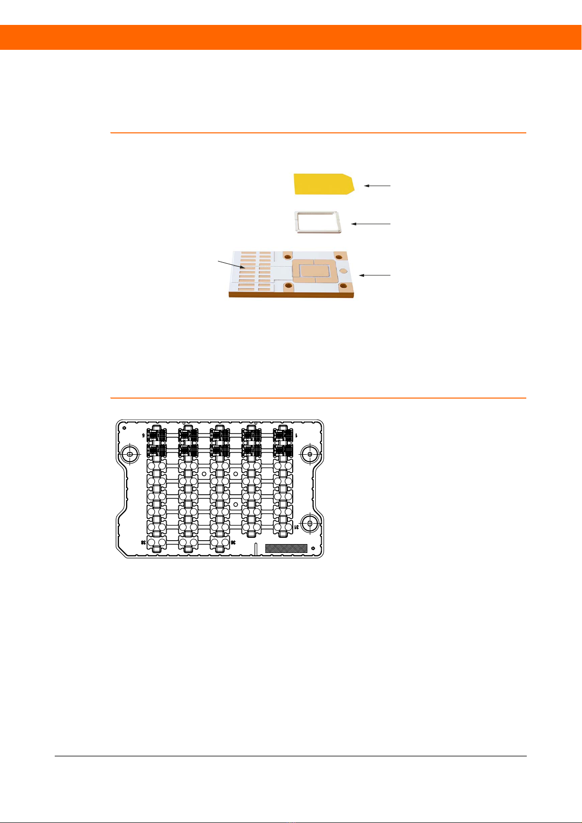
C. OSRAM OSTAR®Projection Power with connecting board
The OSRAM OSTAR®Projection Power devices on a connecting board are
available in three different colors:
• Deep Blue / Blue
•Amber
• Converted Green
Figure 3 shows an overview of the standard OSRAM OSTAR®Projection Power
devices witha connecting board. Amber and (deep) blue devices are covered
with a glass window, the converted green LED is cast in silicone.