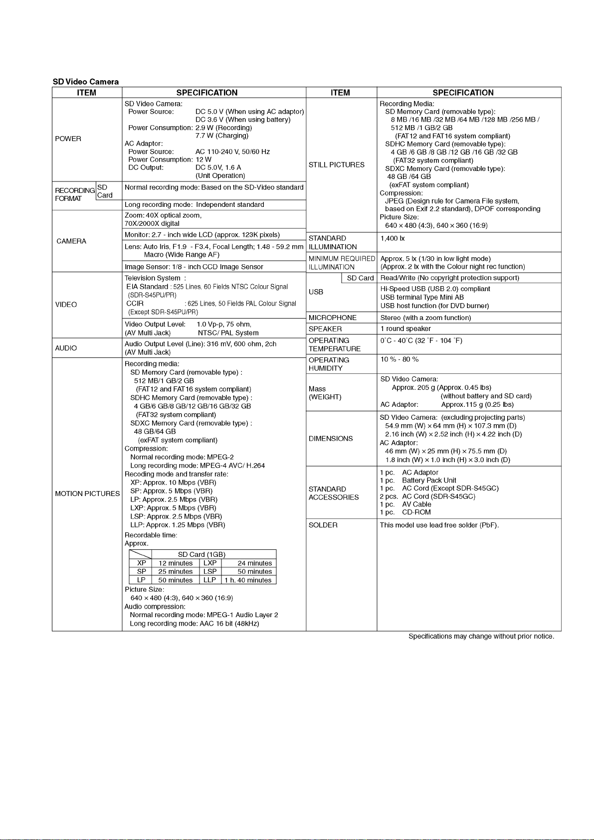
Panasonic SDR-S45EG User manual

© Panasonic Corporation 2010.
Unauthorized copying and distribution is a violation
of law.
ORDER NO.VM1004028CE
SD Video Camera
Model No. SDR-S45EG
SDR-S45EF
SDR-S45EC
SDR-S45EP
SDR-S45EB
SDR-S45EE
SDR-S45GC
SDR-S45GA
SDR-S45GN
SDR-S45PU
SDR-S45PR
VOL.2
Colour
(S)........Silver Type

2
TABLE OF CONTENTS PAGE PAGE
1 Safety Precautions -----------------------------------------------3
1.1. General Guidelines ----------------------------------------3
2Warning--------------------------------------------------------------4
2.1. Prevention of Electrostatic Discharge (ESD)
to Electrostatic Sensitive (ES) Devices---------------4
2.2. Service caution based on legal restrictions----------5
2.3. Caution for AC Cord (For EB/GC/GA) ----------------6
3 Specifications------------------------------------------------------7
4 Service Mode-------------------------------------------------------8
4.1. Lock Search History Indication -------------------------9
4.2. Power ON Self Check Result Display-----------------9
4.3. Lock Search History Clear-----------------------------10
5 Service Fixture & Tools --------------------------------------- 11
5.1. Service Tools and Equipment------------------------- 11
6 Measurements and Adjustments --------------------------12
6.1. Service Positions-----------------------------------------12

3
1 Safety Precautions
1.1. General Guidelines
1. IMPORTANT SAFETY NOTICE
There are special components used in this equipment which are important for safety. These parts are marked by in the
Schematic Diagrams, Circuit Board Layout, Exploded Views and Replacement Parts List. It is essential that these critical parts
should be replaced with manufacturer’s specified parts to prevent X-RADIATION, shock fire, or other hazards. Do not modify
the original design without permission of manufacturer.
2. An Isolation Transformer should always be used during the servicing of AC Adaptor whose chassis is not isolated from the AC
power line. Use a transformer of adequate power rating as this protects the technician from accidents resulting in personal
injury from electrical shocks. It will also protect AC Adaptor from being damaged by accidental shorting that may occur during
servicing.
3. When servicing, observe the original lead dress. If a short circuit is found, replace all parts which have been overheated or
damaged by the short circuit.
4. After servicing, see to it that all the protective devices such as insulation barriers, insulation papers shields are properly
installed.
5. After servicing, make the following leakage current checks to prevent the customer from being exposed to shock hazards.

4
2Warning
2.1. Prevention of Electrostatic Discharge (ESD) to Electrostatic Sensitive
(ES) Devices
Some semiconductor (solid state) devices can be damaged easily by static electricity. Such components commonly are called Elec-
trostatic Sensitive (ES) Devices. Examples of typical ES devices are integrated circuits and some field-effect transistors and semi-
conductor “chip” components. The following techniques should be used to help reduce the incidence of component damage caused
by electrostatic discharge (ESD).
1. Immediately before handling any semiconductor component or semiconductor-equipped assembly, drain off any ESD on your
body by touching a known earth ground. Alternatively, obtain and wear a commercially available discharging ESD wrist strap,
which should be removed for potential shock reasons prior to applying power to the unit under test.
2. After removing an electrical assembly equipped with ES devices, place the assembly on a conductive surface such as alumi-
num foil, to prevent electrostatic charge buildup or exposure of the assembly.
3. Use only a grounded-tip soldering iron to solder or unsolder ES devices.
4. Use only an antistatic solder removal device. Some solder removal devices not classified as “antistatic (ESD protected)” can
generate electrical charge sufficient to damage ES devices.
5. Do not use freon-propelled chemicals. These can generate electrical charges sufficient to damage ES devices.
6. Do not remove a replacement ES device from its protective package until immediately before you are ready to install it. (Most
replacement ES devices are packaged with leads electrically shorted together by conductive foam, aluminum foil or compara-
ble conductive material).
7. Immediately before removing the protective material from the leads of a replacement ES device, touch the protective material
to the chassis or circuit assembly into which the device will be installed.
CAUTION:
Be sure no power is applied to the chassis or circuit, and observe all other safety precautions.
8. Minimize bodily motions when handling unpackaged replacement ES devices. (Otherwise harmless motion such as the
brushing together of your clothes fabric or the lifting of your foot from a carpeted floor can generate static electricity (ESD) suf-
ficient to damage an ES device).

5
2.2. Service caution based on legal restrictions
2.2.1. General description about Lead Free Solder (PbF)
The lead free solder has been used in the mounting process of all electrical components on the printed circuit boards used for this
equipment in considering the globally environmental conservation.
The normal solder is the alloy of tin (Sn) and lead (Pb). On the other hand, the lead free solder is the alloy mainly consists of tin
(Sn), silver (Ag) and Copper (Cu), and the melting point of the lead free solder is higher approx.30 degrees C (86°F) more than that
of the normal solder.
Definition of PCB Lead Free Solder being used
Service caution for repair work using Lead Free Solder (PbF)
• The lead free solder has to be used when repairing the equipment for which the lead free solder is used.
(Definition: The letter of “PbF” is printed on the PCB using the lead free solder.)
• To put lead free solder, it should be well molten and mixed with the original lead free solder.
• Remove the remaining lead free solder on the PCB cleanly for soldering of the new IC.
• Since the melting point of the lead free solder is higher than that of the normal lead solder, it takes the longer time to melt the
lead free solder.
• Use the soldering iron (more than 70W) equipped with the temperature control after setting the temperature at 350±30 degrees
C (662±86°F).
Recommended Lead Free Solder (Service Parts Route.)
• The following 3 types of lead free solder are available through the service parts route.
RFKZ03D01KS-----------(0.3mm 100g Reel)
RFKZ06D01KS-----------(0.6mm 100g Reel)
RFKZ10D01KS-----------(1.0mm 100g Reel)
Note
* Ingredient: tin (Sn), 96.5%, silver (Ag) 3.0%, Copper (Cu) 0.5%, Cobalt (Co) / Germanium (Ge) 0.1 to 0.3%
The letter of “PbF” is printed either foil side or components side on the PCB using the lead free solder.
(See right figure)

6
2.3. Caution for AC Cord
(For EB/GC/GA)
2.3.1. Information for your safety
IMPORTANT
Your attention is drawn to the fact that recording of pre-
recorded tapes or discs or other published or broadcast
material may infringe copyright laws.
WARNING
To reduce the risk of fire or shock hazard, do not expose
this equipment to rain or moisture.
CAUTION
To reduce the risk of fire or shock hazard and annoying
interference, use the recommended accessories only.
FOR YOUR SAFETY
DO NOT REMOVE THE OUTER COVER
To prevent electric shock, do not remove the cover. No user
serviceable parts inside. Refer servicing to qualified service
personnel.
2.3.2. Caution for AC mains lead
For your safety, please read the following text carefully.
This appliance is supplied with a moulded three-pin mains plug
for your safety and convenience.
A 5-ampere fuse is fitted in this plug.
Should the fuse need to be replaced please ensure that the
replacement fuse has a rating of 5 amperes and it is approved
by ASTA or BSI to BS1362
Check for the ASTA mark or the BSI mark on the body of the
fuse.
If the plug contains a removable fuse cover you must ensure
that it is refitted when the fuse is replaced.
If you lose the fuse cover, the plug must not be used until a
replacement cover is obtained.
A replacement fuse cover can be purchased from your local
Panasonic Dealer.
If the fitted moulded plug is unsuitable for the socket outlet in
your home then the fuse should be removed and the plug cut
off and disposed of safety.
There is a danger of severe electrical shock if the cut off plug is
inserted into any 13-ampere socket.
If a new plug is to be fitted please observe the wiring code as
shown below.
If in any doubt, please consult a qualified electrician.
2.3.2.1. Important
The wires in this mains lead are coloured in accordance with
the following code:
As the colours of the wires in the mains lead of this appliance
may not correspond with the coloured markings identifying the
terminals in your plug, proceed as follows:
The wire which is coloured BLUE must be connected to the ter-
minal in the plug which is marked with the letter N or coloured
BLACK.
The wire which is coloured BROWN must be connected to the
terminal in the plug which is marked with the letter L or coloured
RED.
Under no circumstances should either of these wires be con-
nected to the earth terminal of the three pin plug, marked with
the letter E or the Earth Symbol.
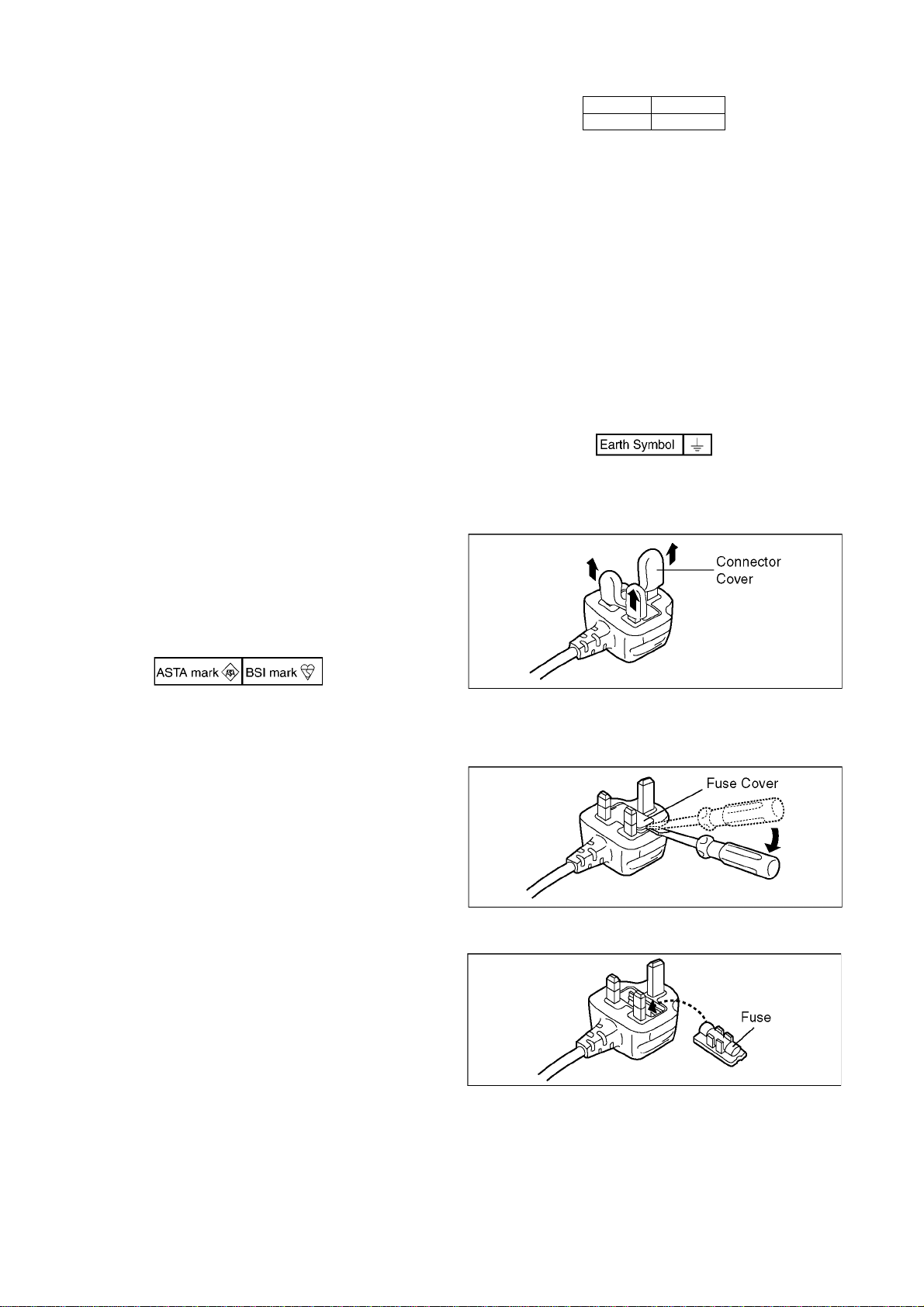
2.3.2.2. Before use
remove the Connector Cover as follows.
2.3.2.3. How to replace the Fuse
1. Remove the Fuse Cover with a screwdriver.
2. Replace the fuse and attach the Fuse cover.
Blue Neutral
Brown Live

7
3 Specifications

8
4 Service Mode
1. Indication method of the service menu
Set the mode switch " Recording" mode.
2. While keep pressing the "Intelligent auto/Manual" button and "Menu" button, hold left the Zoom Lever towards to "[ W ]" posi-
tion for more than 3 seconds until the top screen of the Service Menu being displayed.
Service mode menu
Note:
Do not using service mode except above table of Service Menu.
3. End method of the top screen of the service menu
Push the menu button to end the service mode, and then POWER OFF.
Screen
display Contents Function
1 Factory settings Function to throw a product up in a factory shipment state
4 Lock search history indication Display an error code for three histories saved in EEPROM
5 Power ON self check result dis-
play Power ON self check (function to diagnose correct function of the device and interface
between devices) result display
10 Lock search history clear An error code for three histories in EEPROM is cleared

9
4.1. Lock Search History Indication
1. Select [ 4 ] Lock search history indication.
Operation specifications
Indication contents
• Lock search history indication
Display the camera system error code for three histories saved in EEPROM.
• The error code contents which are displayed
Lock search history indication is finished by POWER OFF.
4.2. Power ON Self Check Result Display
1. Select [ 5 ] Power ON self check result display.
Operation specifications
Indication contents
• Power ON self check result display
Function to diagnose correct function of the device and interface between devices result display.
Display the following communication test result.
- CAM-PWR : Communication test between IC2304 to IC2006
- CAM-UNI : Communication test between IC3401 to IC2006
Display other than “OK” are abnormalities of each lines.
Power ON self check result display is finished by POWER OFF.
Error code Function
51 Focus control is abnormal
52 Zoom control is abnormal
73 High temperature is abnormal
33 Communication between camera to ARM is abnormal

10
4.3. Lock Search History Clear
1. Select [ 10 ] Lock Search History Clear.
Operation specifications
• Lock Search History Clear
An error code for three histories in EEPROM is cleared.
Push the menu button to end the service mode, and then POWER OFF.

11
5 Service Fixture & Tools
5.1. Service Tools and Equipment

12
6 Measurements and Adjustments
6.1. Service Positions
6.1.1. List of the extension cables
Use the following extension cables when checking or adjusting individual circuit boards except module Parts (Main P.C.B.).

13
6.1.2. Checking and repairing individual circuit boards
How to use extension cables.

S-1
S1. About Indication of The Schematic Diagram ............................ S-1
S1.1. Important Safety Notice......................................................... S-1
S2. Voltage Chart ........................................................................... S-2
S2.1. Main P.C.B. ........................................................................... S-2
S3. Block Diagram.......................................................................... S-6
S3.1. System Control Block Diagram ............................................. S-6
S3.2. Audio/Video Block Diagram................................................... S-7
S3.3. Camera Drive Block Diagram................................................ S-8
S3.4. Lens Drive Block Diagram..................................................... S-9
S3.5. Monitor Block Diagram........................................................ S-10
S3.6. Charge Block Diagram........................................................ S-11
S3.7. Power Supply Block Diagram.............................................. S-12
S4. Schematic Diagram................................................................ S-14
S4.1. Main CN Schematic Diagram.............................................. S-14
S4.2. Power Schematic Diagram.................................................. S-18
S4.3. Charge Schematic Diagram................................................ S-22
S4.4. AFE Schematic Diagram ..................................................... S-23
S4.5. Lens Drive Schematic Diagram........................................... S-24
S4.6. Syscon Schematic Diagram................................................ S-26
S4.7. RTC Schematic Diagram .................................................... S-30
S4.8. Video Schematic Diagram................................................... S-32
S4.9. AVIO Schematic Diagram.................................................... S-36
S4.10. MIC Schematic Diagram ................................................... S-37
S4.11. LCD Schematic Diagram................................................... S-38
S4.12. G_Sensor Schematic Diagram.......................................... S-39
S4.13. LED Schematic Diagram................................................... S-39
S5. Print Circuit Board.................................................................. S-40
S5.1. Main P.C.B. ......................................................................... S-40
S5.1.1. Main P.C.B. ...................................................................... S-40
S5.1.2. Main P.C.B. Address Information ..................................... S-44
S6. Abbreviation ........................................................................... S-45
S7. Check Point of The IC............................................................ S-61
S7.1. IC101................................................................................... S-61
S7.2. IC701................................................................................... S-63
S7.3. IC1001................................................................................. S-66
S7.4. IC2006................................................................................. S-68
S7.5. IC2304................................................................................. S-73
S7.6. IC3401................................................................................. S-74
S7.7. IC3402................................................................................. S-86
S8. Replacement Parts List.......................................................... S-88
Table of contents
Service Manual
VM1004028CE
Diagrams and Replacement
Parts List
Vol. 2
(S)...........Silver Type
Colour
Model No.
SDR-S45EG
SDR-S45EF
SDR-S45EC
SDR-S45EP
SDR-S45EB
SDR-S45EE
SDR-S45GC
SDR-S45GA
SDR-S45GN
SDR-S45PU
SDR-S45PR
SD Video Camera
Name of Signal
OFTR FEP This signal is connected
to the FEP schematic diagram.
Circuit name being connected.
6.Use the parts number indicated on the Replacement Parts List .
7.Indication on Schematic diagrams:
5.The voltage being indicated here may be include observational-error (deviation) due to
internal-resistance and/or reactance of equipment. Therefore, handle the value
indicated on here as reference.
4.Although the voltage and waveform available on here is measured with standard frame,
it may be differ from actual measurement due to modification of circuit and so on.
3.The voltage being indicated on the schematic diagram is measured in
"Standard-Playback" mode when there is no specify mode is mentioned.
2.It is only the "Test Round" and no terminal (Pin) is available on the P.C.B.
when the TP (Test Point) indicated as " " mark.
1.Although reference number of the parts is indicated on the P.C.B. drawing and/or
schematic diagrams, it is NOT mounted on the P.C.B. when it is displayed with "$" mark.
FOR SAFETY. WHEN REPLACING ANY OF THESE COMPONENTS USE ONLY THE SAME TYPE.
COMPONENTS IDENTIFIED WITH THE MARK HAVE THE SPECIAL CHARACTERISTICS
S1. About Indication of The Schematic Diagram
S1.1. Important Safety Notice

S-2
S2. Voltage Chart
S2.1. Main P.C.B.
Note) Indicated voltage values are the standard values for the unit measured by the DC electronic circuit tester (high-impedance) with the chassis taken as standard.
Therefore, there may exist some errors in the voltage values, depending on the internal impedance of the DC circuit tester.
REF No.
PIN No.
REC PB EE
IC101 1 1.7 1.7
IC101 2 3.3 3.3
IC101 3 0 0
IC101 4 1.1 1.1
IC101 5 0 0
IC101 6 3 3
IC101 7 - -
IC101 8 1.1 1.1
IC101 9 0 0
IC101 10 - -
IC101 11 1.4 1.4
IC101 12 3.3 3.3
IC101 13 0 0
IC101 14 0 0
IC101 15 - -
IC101 16 3 3
IC101 17 - -
IC101 18 - -
IC101 19 - -
IC101 20 - -
IC101 21 3 3
IC101 22 3 3
IC101 23 3 3
IC101 24 0.1 0.1
IC101 25 0.3 0.3
IC101 26 12 12
IC101 27 - -
IC101 28 - -
IC101 29 - -
IC101 30 - -
IC101 31 3.3 3.3
IC101 32 - -
IC101 33 0 0
IC101 34 0 0
IC101 35 - -
IC101 36 - -
IC101 37 3 3
IC101 38 0 0
IC101 39 0 0
IC101 40 0 0
IC101 41 - -
IC101 42 - -
IC101 43 - -
IC101 44 3 3
IC101 45 0 0
IC101 46 0 0
IC101 47 - -
IC101 48 - -
IC101 49 - -
IC101 50 3 3
IC101 51 0 0
IC101 52 - -
IC101 53 - -
IC101 54 - -
IC101 55 0 0
IC101 56 2 2
IC101 57 3 3
IC101 58 0 0
IC101 59 0 0
IC101 60 3 3
IC101 61 3 3
IC101 62 1.5 1.5
IC101 63 -7.5 -7.5
IC101 64 0 0
IC101 65 2.9 2.9
IC101 66 1.3 1.3
REF No.
PIN No.
REC PB EE
IC101 67 0 0
IC101 68 2 2
IC101 69 0 0
IC101 70 0 0
IC101 71 2.9 2.9
IC101 72 0 0
IC101 73 - -
IC101 74 - -
IC101 75 2.9 2.9
IC101 76 0 0
IC101 77 2 2
IC101 78 2 2
IC101 79 1.8 1.8
IC101 80 0 0
IC101 81 2 2
IC101 82 1 1
IC101 83 3 3
IC101 84 2.9 2.9
IC101 85 12 12
IC102 1 4.9 4.9
IC102 2 0 0
IC102 3 - -
IC102 4 3.3 3.3
IC102 5 4.9 4.9
IC601 1 1.3 1.3 1.3
IC601 2 - - -
IC601 3 0 0 0
IC601 4 3 3 3
IC601 5 0 0 0
IC601 6 0 0 0
IC601 7 0 0 0
IC601 8 3 3 3
IC601 9 2.8 2.8 2.8
IC601 10 0 0 0
IC601 11 0.9 0.9 0.9
IC601 12 - - -
IC601 13 - - -
IC601 14 0.4 0.4 0.4
IC601 15 1 1 1
IC601 16 0.9 0.9 0.9
IC601 17 0 0 0
IC601 18 1.2 1.2 1.2
IC601 19 0.6 0.6 0.6
IC601 20 0.7 0.7 0.7
IC601 21 0.7 0.7 0.7
IC601 22 0.7 0.7 0.7
IC601 23 1.8 1.8 1.8
IC601 24 4.9 4.9 4.9
IC601 25 2.5 2.5 2.5
IC601 26 2.5 2.5 2.5
IC601 27 2.5 2.5 2.5
IC601 28 0 0 0
IC601 29 4.6 4.6 4.6
IC601 30 4.5 4.5 4.5
IC601 31 0.8 0.8 0.8
IC601 32 0.3 0.3 0.3
IC601 33 4.9 4.9 4.9
IC601 34 4.3 4.3 4.3
IC601 35 2.8 2.8 2.8
IC601 36 2.6 2.6 2.6
IC601 37 0 0 0
IC601 38 3 3 3
IC601 39 - - -
IC601 40 - - -
IC601 41 - - -
IC601 42 - - -
REF No.
PIN No.
REC PB EE
IC601 43 - - -
IC601 44 - - -
IC601 45 2.9 2.9 2.9
IC601 46 2.9 2.9 2.9
IC601 47 - - -
IC601 48 - - -
IC601 49 0 0 0
IC601 50 0 0 0
IC601 51 - - -
IC601 52 - - -
IC601 53 - - -
IC601 54 - - -
IC601 55 0.2 0.2 0.2
IC601 56 3 3 3
IC601 57 1.4 1.4 1.4
IC601 58 1.4 1.4 1.4
IC601 59 - - -
IC601 60 0 0 0
IC601 61 - - -
IC601 62 2.2 2.2 2.2
IC601 63 0 0 0
IC601 64 - - -
IC701 1 0 0
IC701 2 2.8 2.8
IC701 3 1.4 1.4
IC701 4 2.8 2.8
IC701 5 0 0
IC701 6 1.8 1.8
IC701 7 - -
IC701 8 - -
IC701 9 0 0
IC701 10 2.8 2.8
IC701 11 2.8 2.8
IC701 12 - -
IC701 13 - -
IC701 14 2.8 2.8
IC701 15 3 3
IC701 16 - -
IC701 17 3 3
IC701 18 1.4 1.4
IC701 19 - -
IC701 20 3 3
IC701 21 1.4 1.4
IC701 22 0 0
IC701 23 - -
IC701 24 2.9 2.9
IC701 25 - -
IC701 26 4.9 4.9
IC701 27 3 3
IC701 28 - -
IC701 29 - -
IC701 30 0 0
IC701 31 0 0
IC701 32 - -
IC701 33 0 0
IC701 34 - -
IC701 35 0 0
IC701 36 - -
IC701 37 - -
IC701 38 - -
IC701 39 - -
IC701 40 2.6 2.6
IC701 41 - -
IC701 42 3 3
IC701 43 - -
IC701 44 - -
REF No.
PIN No.
REC PB EE
IC701 45 - -
IC701 46 2.8 2.8
IC701 47 1.4 1.4
IC701 48 1.4 1.4
IC701 49 1.4 1.4
IC701 50 1.4 1.4
IC701 51 2.8 2.8
IC701 52 - -
IC701 53 2.8 2.8
IC701 54 1.9 1.9
IC701 55 2.8 2.8
IC701 56 1.4 1.4
IC701 57 2.2 2.2
IC701 58 0 0
IC701 59 0 0
IC701 60 - -
IC701 61 0 0
IC701 62 - -
IC701 63 - -
IC701 64 - -
IC701 65 - -
IC701 66 1.5 1.5
IC701 67 - -
IC701 68 - -
IC701 69 2.9 2.9
IC701 70 - -
IC701 71 1.4 1.4
IC701 72 2 2
IC701 73 2.8 2.8
IC701 74 2 2
IC701 75 - -
IC701 76 0 0
IC701 77 3 3
IC701 78 3 3
IC701 79 - -
IC701 80 1.4 1.4
IC701 81 2 2
IC701 82 1.4 1.4
IC701 83 - -
IC701 84 1.4 1.4
IC701 85 2 2
IC701 86 1.4 1.4
IC701 87 0 0
IC701 88 3 3
IC701 89 1.4 1.4
IC701 90 1.4 1.4
IC701 91 0 0
IC701 92 1.4 1.4
IC701 93 1.5 1.5
IC701 94 0 0
IC701 95 - -
IC701 96 1.5 1.5
IC701 97 - -
IC701 98 1.5 1.5
IC701 99 1.5 1.5
IC701 100 - -
IC701 101 1.4 1.4
IC701 102 1.4 1.4
IC701 103 1.4 1.4
IC701 104 1.4 1.4
IC701 105 1.4 1.4
IC701 106 - -
IC701 107 1.4 1.4
IC701 108 0 0
IC701 109 - -
IC701 110 3 3
REF No.
PIN No.
REC PB EE
IC701 111 - -
IC701 112 - -
IC701 113 - -
IC701 114 - -
IC701 115 - -
IC701 116 - -
IC701 117 - -
IC701 118 0 0
IC701 119 - -
IC701 120 2.6 2.6
IC1001 1 0 0 0
IC1001 2 0 0 0
IC1001 3 5.2 5.2 5.2
IC1001 4 5.2 5.2 5.2
IC1001 5 0 0 0
IC1001 6 8.5 8.5 8.5
IC1001 7 8.5 8.5 8.5
IC1001 8 8.5 8.5 8.5
IC1001 9 1.8 1.8 1.8
IC1001 10 1.8 1.8 1.8
IC1001 11 0 0 0
IC1001 12 0 0 0
IC1001 13 1.1 1.1 1.1
IC1001 14 0.6 0.6 0.6
IC1001 15 1.2 1.2 1.2
IC1001 16 0.6 0.6 0.6
IC1001 17 1.5 1.5 1.5
IC1001 18 0 0 0
IC1001 19 1.5 1.5 1.5
IC1001 20 2.3 2.3 2.3
IC1001 21 0 0 0
IC1001 22 - - -
IC1001 23 - - -
IC1001 24 2.6 2.6 2.6
IC1001 25 8.5 8.5 8.5
IC1001 26 8.5 8.5 8.5
IC1001 27 1.2 1.2 1.2
IC1001 28 1.2 1.2 1.2
IC1001 29 0 0 0
IC1001 30 0 0 0
IC1001 31 0 0 0
IC1001 32 0 0 0
IC1001 33 1.1 1.1 1.1
IC1001 34 1.1 1.1 1.1
IC1001 35 8.5 8.5 8.5
IC1001 36 8.5 8.5 8.5
IC1001 37 0 0 0
IC1001 38 1.2 1.2 1.2
IC1001 39 3 3 3
IC1001 40 0.6 0.6 0.6
IC1001 41 1.2 1.2 1.2
IC1001 42 0.6 0.6 0.6
IC1001 43 1.2 1.2 1.2
IC1001 44 0.6 0.6 0.6
IC1001 45 8.5 8.5 8.5
IC1001 46 8.5 8.5 8.5
IC1001 47 3.3 3.3 3.3
IC1001 48 3.3 3.3 3.3
IC1001 49 0 0 0
IC1001 50 0 0 0
IC1001 51 3.3 3.3 3.3
IC1001 52 3.3 3.3 3.3
IC1001 53 3 3 3
IC1001 54 3 3 3
IC1001 55 1.5 1.5 1.5
IC1001 56 0.7 0.7 0.7
REF No.
PIN No.
REC PB EE
IC1001 57 1.4 1.4 1.4
IC1001 58 0 0 0
IC1001 59 0 0 0
IC1001 60 2.6 2.6 2.6
IC1001 61 1.9 1.9 1.9
IC1001 62 8.6 8.6 8.6
IC1001 63 1.2 1.2 1.2
IC1001 64 0.6 0.6 0.6
IC1001 65 2.4 2.4 2.4
IC1001 66 8.6 8.6 8.6
IC1001 67 1 1 1
IC1001 68 2.8 2.8 2.8
IC1001 69 5 5 5
IC1001 70 1.2 1.2 1.2
IC1001 71 5 5 5
IC1001 72 0.6 0.6 0.6
IC1001 73 0.1 0.1 0.1
IC1001 74 0 0 0
IC1001 75 0 0 0
IC1001 76 0 0 0
IC1001 77 0 0 0
IC1001 78 0 0 0
IC1001 79 0 0 0
IC1001 80 0 0 0
IC1001 81 0 0 0
IC1001 82 0 0 0
IC1301 1 2.8 2.8 2.8
IC1301 2 0 0 0
IC1301 3 1.2 1.2 1.2
IC1301 4 4.9 4.9 4.9
IC1301 5 4.9 4.9 4.9
IC1371 1 1.6 1.6 1.6
IC1371 2 12 12 12
IC1371 3 1.4 1.4 1.4
IC1371 4 1.6 1.6 1.6
IC1371 5 -12.5 -12.5 -12.5
IC1371 6 -7.6 -7.6 -7.6
IC1371 7 0 0 0
IC1371 8 12 12 12
IC1411 1 - - -
IC1411 2 0 0 0
IC1411 3 2.8 2.8 2.8
IC1411 4 4.9 4.9 4.9
IC1411 5 3.2 3.2 3.2
IC1412 1 4.9 4.9 4.9
IC1412 2 0 0 0
IC1412 3 - - -
IC1412 4 3 3 3
IC1412 5 4.9 4.9 4.9
IC1413 1 4.9 4.9 4.9
IC1413 2 0 0 0
IC1413 3 - - -
IC1413 4 3 3 3
IC1413 5 4.9 4.9 4.9
IC1414 1 4.9 4.9 4.9
IC1414 2 4.9 4.9 4.9
IC1414 3 - - -
IC1414 4 0 0 0
IC1503 1 4.8 4.8 4.8
IC1503 2 4.8 4.8 4.8
IC1503 3 5 5 5
IC1503 4 3.2 3.2 3.2
IC1503 5 8.8 8.8 8.8
IC1503 6 8.8 8.8 8.8
IC1503 7 3.2 3.2 3.2
IC1503 8 3.2 3.2 3.2
REF No.
PIN No.
REC PB EE
IC1503 9 0 0 0
IC1503 10 0 0 0
IC1503 11 0 0 0
IC1503 12 0.7 0.7 0.7
IC1503 13 0.7 0.7 0.7
IC1503 14 1.2 1.2 1.2
IC1503 15 2.8 2.8 2.8
IC1503 16 3.2 3.2 3.2
IC1503 17 8.8 8.8 8.8
IC1503 18 3.2 3.2 3.2
IC1503 19 8.6 8.6 8.6
IC1503 20 0 0 0
IC1503 21 3.5 3.5 3.5
IC1503 22 1.8 1.8 1.8
IC1503 23 2.8 2.8 2.8
IC1503 24 0 0 0
IC1503 25 0 0 0
IC1503 26 4.8 4.8 4.8
IC1503 27 4.9 4.9 4.9
IC1503 28 4.8 4.8 4.8
IC1503 29 4.8 4.8 4.8
IC1503 30 4.8 4.8 4.8
IC1503 31 8.6 8.6 8.6
IC1503 32 8.6 8.6 8.6
IC1504 1 3 3 3
IC1504 2 0 0 0
IC1504 3 0 0 0
IC1504 4 0 0 0
IC1504 5 0 0 0
IC1504 6 0 0 0
IC1504 7 3 3 3
IC1504 8 3.2 3.2 3.2
IC1505 1 3 3 3
IC1505 2 0 0 0
IC1505 3 3 3 3
IC1505 4 1 1 1
IC1505 5 3.2 3.2 3.2
IC2001 1 0 0 0
IC2001 2 3 3 3
IC2001 3 1.2 1.2 1.2
IC2001 4 3 3 3
IC2002 1 2.8 2.8 2.8
IC2002 2 3 3 3
IC2002 3 3 3 3
IC2002 4 0 0 0
IC2002 5 3 3 3
IC2002 6 2.8 2.8 2.8
IC2002 7 3 3 3
IC2002 8 3 3 3
IC2006 A1 3 3 3
IC2006 A2 3 3 3
IC2006 A3 - - -
IC2006 A4 3 3 3
IC2006 A5 3 3 3
IC2006 A6 - - -
IC2006 A7 - - -
IC2006 A8 - - -
IC2006 A9 - - -
IC2006 A10 - - -
IC2006 A11 - - -
IC2006 A12 - - -
IC2006 A13 - - -
IC2006 A14 - - -
IC2006 A15 3 3 3
IC2006 A16 2.8 2.8 2.8
IC2006 A17 - - -

S-3
REF No.
PIN No.
REC PB EE
IC2006 A18 - - -
IC2006 A19 3 3 3
IC2006 A20 3 3 3
IC2006 B1 3 3 3
IC2006 B2 3 3 3
IC2006 B3 - - -
IC2006 B4 2.4 2.4 2.4
IC2006 B5 3 3 3
IC2006 B6 - - -
IC2006 B7 - - -
IC2006 B8 2.2 2.2 2.2
IC2006 B9 - - -
IC2006 B10 - - -
IC2006 B11 - - -
IC2006 B12 - - -
IC2006 B13 2.8 2.8 2.8
IC2006 B14 2.8 2.8 2.8
IC2006 B15 1.4 1.4 1.4
IC2006 B16 2.8 2.8 2.8
IC2006 B17 - - -
IC2006 B18 - - -
IC2006 B19 3 3 3
IC2006 B20 3 3 3
IC2006 C1 3 3 3
IC2006 C2 - - -
IC2006 C3 3 3 3
IC2006 C4 4.2 4.2 4.2
IC2006 C5 - - -
IC2006 C6 3 3 3
IC2006 C7 - - -
IC2006 C8 0.6 0.6 0.6
IC2006 C9 - - -
IC2006 C10 - - -
IC2006 C11 - - -
IC2006 C12 - - -
IC2006 C13 3 3 3
IC2006 C14 - - -
IC2006 C15 3 3 3
IC2006 C16 2.8 2.8 2.8
IC2006 C17 1.4 1.4 1.4
IC2006 C18 3 3 3
IC2006 C19 3 3 3
IC2006 C20 3 3 3
IC2006 D1 - - -
IC2006 D2 - - -
IC2006 D3 - - -
IC2006 D4 3 3 3
IC2006 D5 0 0 0
IC2006 D6 - - -
IC2006 D7 - - -
IC2006 D8 1.5 1.5 1.5
IC2006 D9 0 0 0
IC2006 D10 - - -
IC2006 D11 3 3 3
IC2006 D12 - - -
IC2006 D13 - - -
IC2006 D14 0 0 0
IC2006 D15 2.8 2.8 2.8
IC2006 D16 2.8 2.8 2.8
IC2006 D17 3 3 3
IC2006 D18 - - -
IC2006 D19 - - -
IC2006 D20 - - -
IC2006 E1 - - -
IC2006 E2 - - -
IC2006 E3 - - -
REF No.
PIN No.
REC PB EE
IC2006 E4 0 0 0
IC2006 E5 0 0 0
IC2006 E17 - - -
IC2006 E18 - - -
IC2006 E19 0 0 0
IC2006 E20 0 0 0
IC2006 F1 - - -
IC2006 F2 2.8 2.8 2.8
IC2006 F3 2.9 2.9 2.9
IC2006 F4 0 0 0
IC2006 F17 0 0 0
IC2006 F18 - - -
IC2006 F19 0 0 0
IC2006 F20 0 0 0
IC2006 G1 - - -
IC2006 G2 2.9 2.9 2.9
IC2006 G3 2.8 2.8 2.8
IC2006 G4 3 3 3
IC2006 G17 1.8 1.8 1.8
IC2006 G18 - - -
IC2006 G19 - - -
IC2006 G20 2.8 2.8 2.8
IC2006 H1 1.5 1.5 1.5
IC2006 H2 1.2 1.2 1.2
IC2006 H3 1.6 1.6 1.6
IC2006 H4 1.8 1.8 1.8
IC2006 H17 - - -
IC2006 H18 0 0 0
IC2006 H19 2.8 2.8 2.8
IC2006 H20 - - -
IC2006 J1 0 0 0
IC2006 J2 - - -
IC2006 J3 3 3 3
IC2006 J4 - - -
IC2006 J17 1.8 1.8 1.8
IC2006 J18 0 0 0
IC2006 J19 0 0 0
IC2006 J20 - - -
IC2006 K1 - - -
IC2006 K2 0 0 0
IC2006 K3 0 0 0
IC2006 K4 3 3 3
IC2006 K17 0 0 0
IC2006 K18 0 0 0
IC2006 K19 - - -
IC2006 K20 0 0 0
IC2006 L1 - - -
IC2006 L2 2.8 2.8 2.8
IC2006 L3 - - -
IC2006 L4 3 3 3
IC2006 L17 - - -
IC2006 L18 - - -
IC2006 L19 - - -
IC2006 L20 - - -
IC2006 M1 0 0 0
IC2006 M2 - - -
IC2006 M3 - - -
IC2006 M4 1.8 1.8 1.8
IC2006 M17 - - -
IC2006 M18 - - -
IC2006 M19 - - -
IC2006 M20 - - -
IC2006 N1 1.5 1.5 1.5
IC2006 N2 3 3 3
IC2006 N3 - - -
IC2006 N4 1.5 1.5 1.5
REF No.
PIN No.
REC PB EE
IC2006 N17 - - -
IC2006 N18 - - -
IC2006 N19 - - -
IC2006 N20 - - -
IC2006 P1 - - -
IC2006 P2 - - -
IC2006 P3 2.8 2.8 2.8
IC2006 P4 - - -
IC2006 P17 - - -
IC2006 P18 - - -
IC2006 P19 - - -
IC2006 P20 - - -
IC2006 R1 0 0 0
IC2006 R2 - - -
IC2006 R3 - - -
IC2006 R4 0 0 0
IC2006 R17 0 0 0
IC2006 R18 - - -
IC2006 R19 0 0 0
IC2006 R20 - - -
IC2006 T1 - - -
IC2006 T2 - - -
IC2006 T3 - - -
IC2006 T4 - - -
IC2006 T17 - - -
IC2006 T18 - - -
IC2006 T19 2.8 2.8 2.8
IC2006 T20 2.8 2.8 2.8
IC2006 U1 2.8 2.8 2.8
IC2006 U2 - - -
IC2006 U3 2.8 2.8 2.8
IC2006 U4 3 3 3
IC2006 U5 2.8 2.8 2.8
IC2006 U6 3 3 3
IC2006 U7 0 0 0
IC2006 U8 - - -
IC2006 U9 0 0 0
IC2006 U10 0.1 0.1 0.1
IC2006 U11 3 3 3
IC2006 U12 3 3 3
IC2006 U13 0 0 0
IC2006 U14 2.8 2.8 2.8
IC2006 U15 - - -
IC2006 U16 - - -
IC2006 U17 1.8 1.8 1.8
IC2006 U18 - - -
IC2006 U19 2.8 2.8 2.8
IC2006 U20 2.8 2.8 2.8
IC2006 V1 - - -
IC2006 V2 2.8 2.8 2.8
IC2006 V3 3 3 3
IC2006 V4 2.9 2.9 2.9
IC2006 V5 - - -
IC2006 V6 1.5 1.5 1.5
IC2006 V7 - - -
IC2006 V8 0 0 0
IC2006 V9 2.8 2.8 2.8
IC2006 V10 - - -
IC2006 V11 - - -
IC2006 V12 2.6 2.6 2.6
IC2006 V13 2.8 2.8 2.8
IC2006 V14 - - -
IC2006 V15 - - -
IC2006 V16 - - -
IC2006 V17 - - -
IC2006 V18 1.8 1.8 1.8
REF No.
PIN No.
REC PB EE
IC2006 V19 0 0 0
IC2006 V20 - - -
IC2006 W1 3 3 3
IC2006 W2 3 3 3
IC2006 W3 2.9 2.9 2.9
IC2006 W4 2.9 2.9 2.9
IC2006 W5 - - -
IC2006 W6 2.8 2.8 2.8
IC2006 W7 - - -
IC2006 W8 - - -
IC2006 W9 - - -
IC2006 W10 - - -
IC2006 W11 1.2 1.2 1.2
IC2006 W12 - - -
IC2006 W13 3 3 3
IC2006 W14 2.6 2.6 2.6
IC2006 W15 - - -
IC2006 W16 - - -
IC2006 W17 2.8 2.8 2.8
IC2006 W18 - - -
IC2006 W19 1.8 1.8 1.8
IC2006 W20 1.8 1.8 1.8
IC2006 Y1 3 3 3
IC2006 Y2 3 3 3
IC2006 Y3 0 0 0
IC2006 Y4 - - -
IC2006 Y5 3 3 3
IC2006 Y6 - - -
IC2006 Y7 - - -
IC2006 Y8 2.8 2.8 2.8
IC2006 Y9 - - -
IC2006 Y10 - - -
IC2006 Y11 2.8 2.8 2.8
IC2006 Y12 3 3 3
IC2006 Y13 2.8 2.8 2.8
IC2006 Y14 - - -
IC2006 Y15 - - -
IC2006 Y16 - - -
IC2006 Y17 - - -
IC2006 Y18 - - -
IC2006 Y19 1.8 1.8 1.8
IC2006 Y20 1.8 1.8 1.8
IC2302 1 8.6 8.6 8.6
IC2302 2 8.6 8.6 8.6
IC2302 3 8.6 8.6 8.6
IC2302 4 0 0 0
IC2302 5 3.2 3.2 3.2
IC2302 6 3.2 3.2 3.2
IC2304 1 0 0 0
IC2304 2 1 1 1
IC2304 3 1.4 1.4 1.4
IC2304 4 0 0 0
IC2304 5 2.8 2.8 2.8
IC2304 6 1.4 1.4 1.4
IC2304 7 2.8 2.8 2.8
IC2304 8 3.2 3.2 3.2
IC2304 9 2.8 2.8 2.8
IC2304 10 1 1 1
IC2304 11 0 0 0
IC2304 12 1.6 1.6 1.6
IC3401 A1 0 0 0
IC3401 A2 0 0 0
IC3401 A3 1.2 1.2 1.2
IC3401 A4 1.8 1.8 1.8
IC3401 A5 0.8 0.8 0.8
IC3401 A6 0 0 0
REF No.
PIN No.
REC PB EE
IC3401 A7 1.8 1.8 1.8
IC3401 A8 0 0 0
IC3401 A9 0.1 1.4 0.1
IC3401 A10 - - -
IC3401 A11 0 0 0
IC3401 A12 1.1 1.1 1.1
IC3401 A13 1.2 1.2 1.2
IC3401 A14 - - -
IC3401 A15 - - -
IC3401 A16 - - -
IC3401 A17 - - -
IC3401 A18 - - -
IC3401 A19 - - -
IC3401 A20 - - -
IC3401 A21 - - -
IC3401 A22 - - -
IC3401 A23 - - -
IC3401 A24 0 0 0
IC3401 A25 0 0 0
IC3401 A26 0 0 0
IC3401 AA1 - - -
IC3401 AA2 - - -
IC3401 AA3 3 3 3
IC3401 AA4 - - -
IC3401 AA5 2.8 2.8 2.8
IC3401 AA22 - - -
IC3401 AA23 - - -
IC3401 AA24 - - -
IC3401 AA25 - - -
IC3401 AA26 - - -
IC3401 AB1 0 0 0
IC3401 AB2 3 3 3
IC3401 AB3 - - -
IC3401 AB4 0 0 0
IC3401 AB5 0 0 0
IC3401 AB6 - - -
IC3401 AB7 0 0 0
IC3401 AB8 - - -
IC3401 AB9 1.8 1.8 1.8
IC3401 AB10 1.8 1.8 1.8
IC3401 AB11 1.8 1.8 1.8
IC3401 AB12 - - -
IC3401 AB13 - - -
IC3401 AB14 - - -
IC3401 AB15 - - -
IC3401 AB16 - - -
IC3401 AB17 3 3 3
IC3401 AB18 3 3 3
IC3401 AB19 - - -
IC3401 AB20 - - -
IC3401 AB21 - - -
IC3401 AB22 0 0 0
IC3401 AB23 - - -
IC3401 AB24 - - -
IC3401 AB25 - - -
IC3401 AB26 1.8 1.8 1.8
IC3401 AC1 1.2 1.2 1.2
IC3401 AC2 1.2 1.2 1.2
IC3401 AC3 0 0 0
IC3401 AC4 0 0 0
IC3401 AC5 - - -
IC3401 AC6 2.8 2.8 2.8
IC3401 AC7 0 0 0
IC3401 AC8 - - -
IC3401 AC9 2.8 2.8 2.8
IC3401 AC10 2.8 2.8 2.8
REF No.
PIN No.
REC PB EE
IC3401 AC11 - - -
IC3401 AC12 - - -
IC3401 AC13 - - -
IC3401 AC14 - - -
IC3401 AC15 - - -
IC3401 AC16 - - -
IC3401 AC17 3 3 3
IC3401 AC18 - - -
IC3401 AC19 - - -
IC3401 AC20 - - -
IC3401 AC21 - - -
IC3401 AC22 - - -
IC3401 AC23 0 0 0
IC3401 AC24 - - -
IC3401 AC25 1.2 1.2 1.2
IC3401 AC26 1.2 1.2 1.2
IC3401 AD1 1.8 1.8 1.8
IC3401 AD2 1.2 1.2 1.2
IC3401 AD3 0 0 0
IC3401 AD4 0 0 0
IC3401 AD5 - - -
IC3401 AD6 - - -
IC3401 AD7 - - -
IC3401 AD8 - - -
IC3401 AD9 - - -
IC3401 AD10 - - -
IC3401 AD11 - - -
IC3401 AD12 - - -
IC3401 AD13 - - -
IC3401 AD14 - - -
IC3401 AD15 3 3 3
IC3401 AD16 2.8 2.8 2.8
IC3401 AD17 - - -
IC3401 AD18 - - -
IC3401 AD19 - - -
IC3401 AD20 - - -
IC3401 AD21 - - -
IC3401 AD22 - - -
IC3401 AD23 1.2 1.2 1.2
IC3401 AD24 0 0 0
IC3401 AD25 1.2 1.2 1.2
IC3401 AD26 1.2 1.2 1.2
IC3401 AE1 0 0 0
IC3401 AE2 0 0 0
IC3401 AE3 1.2 1.2 1.2
IC3401 AE4 0 0 0
IC3401 AE5 - - -
IC3401 AE6 - - -
IC3401 AE7 - - -
IC3401 AE8 0 0 0
IC3401 AE9 - - -
IC3401 AE10 - - -
IC3401 AE11 - - -
IC3401 AE12 0 0 0
IC3401 AE13 3 3 3
IC3401 AE14 - - -
IC3401 AE14 - - -
IC3401 AE15 - - -
IC3401 AE16 - - -
IC3401 AE17 2.8 2.8 2.8
IC3401 AE18 - - -
IC3401 AE19 - - -
IC3401 AE20 - - -
IC3401 AE21 - - -
IC3401 AE22 - - -
IC3401 AE23 1.2 1.2 1.2
REF No.
PIN No.
REC PB EE
IC3401 AE24 0 0 0
IC3401 AE25 0 0 0
IC3401 AE26 0 0 0
IC3401 AF1 0 0 0
IC3401 AF2 0 0 0
IC3401 AF3 1.2 1.2 1.2
IC3401 AF4 0 0 0
IC3401 AF5 - - -
IC3401 AF6 0 0 0
IC3401 AF7 - - -
IC3401 AF8 1.8 1.8 1.8
IC3401 AF9 0 0 0
IC3401 AF10 - - -
IC3401 AF11 2.4 2.4 2.4
IC3401 AF12 3 3 3
IC3401 AF13 0 0 0
IC3401 AF15 0 0 0
IC3401 AF16 - - -
IC3401 AF17 2.8 2.8 2.8
IC3401 AF18 3 3 3
IC3401 AF19 - - -
IC3401 AF20 - - -
IC3401 AF21 1.2 1.2 1.2
IC3401 AF22 - - -
IC3401 AF23 1.8 1.8 1.8
IC3401 AF24 0 0 0
IC3401 AF25 0 0 0
IC3401 AF26 0 0 0
IC3401 B1 0 0 0
IC3401 B2 0 0 0
IC3401 B3 1.2 1.2 1.2
IC3401 B4 0 0 0
IC3401 B5 - - -
IC3401 B6 1 1 1
IC3401 B7 3 3 3
IC3401 B8 0 0 0
IC3401 B9 0.9 0.9 0.9
IC3401 B10 0 0 0
IC3401 B11 1.8 1.8 1.8
IC3401 B12 - - -
IC3401 B13 - - -
IC3401 B14 - - -
IC3401 B15 - - -
IC3401 B16 - - -
IC3401 B17 - - -
IC3401 B18 - - -
IC3401 B19 - - -
IC3401 B20 0.1 0.1 0.1
IC3401 B21 0.3 0.3 0.3
IC3401 B22 - - -
IC3401 B23 3 3 3
IC3401 B24 0 0 0
IC3401 B25 0 0 0
IC3401 B26 0 0 0
IC3401 C1 0 0 0
IC3401 C2 0 0 0
IC3401 C3 0 0 0
IC3401 C4 0 0 0
IC3401 C5 1.2 1.2 1.2
IC3401 C6 1.2 1.2 1.2
IC3401 C7 3 3 3
IC3401 C8 0 0 0
IC3401 C9 0 0 0
IC3401 C10 0 0 0
IC3401 C11 0.6 0.6 0.6
IC3401 C12 - - -

S-4
REF No.
PIN No.
REC PB EE
IC3401 C13 - - -
IC3401 C14 - - -
IC3401 C15 - - -
IC3401 C16 1.4 1.4 1.4
IC3401 C17 - - -
IC3401 C18 - - -
IC3401 C19 - - -
IC3401 C20 - - -
IC3401 C21 - - -
IC3401 C22 0 0 0
IC3401 C23 0 0 0
IC3401 C24 0 0 0
IC3401 C25 1.2 1.2 1.2
IC3401 C26 1.2 1.2 1.2
IC3401 D1 1.8 1.8 1.8
IC3401 D2 1.8 1.8 1.8
IC3401 D3 - - -
IC3401 D4 0 0 0
IC3401 D5 - - -
IC3401 D6 3 3 3
IC3401 D7 3 3 3
IC3401 D8 0 0 0
IC3401 D9 - - -
IC3401 D10 0.6 0 0.6
IC3401 D11 - - -
IC3401 D12 3 3 3
IC3401 D13 - - -
IC3401 D15 - - -
IC3401 D15 1.4 1.4 1.4
IC3401 D16 2.8 2.8 2.8
IC3401 D17 - - -
IC3401 D18 - - -
IC3401 D19 - - -
IC3401 D20 - - -
IC3401 D21 0 0 0
IC3401 D22 1.2 1.2 1.2
IC3401 D23 0 0 0
IC3401 D24 1.2 1.2 1.2
IC3401 D25 1.2 1.2 1.2
IC3401 D26 1.8 1.8 1.8
IC3401 E1 - - -
IC3401 E2 - - -
IC3401 E3 - - -
IC3401 E4 - - -
IC3401 E5 0 0 0
IC3401 E6 3 3 3
IC3401 E7 0 0 0
IC3401 E8 3 3 3
IC3401 E9 1.8 1.8 1.8
IC3401 E10 - - -
IC3401 E11 - - -
IC3401 E12 3 3 3
IC3401 E13 - - -
IC3401 E14 - - -
IC3401 E15 - - -
IC3401 E16 3 3 3
IC3401 E17 - - -
IC3401 E18 - - -
IC3401 E19 0.1 0.1 0.1
IC3401 E20 0 0 0
IC3401 E21 1.2 1.2 1.2
IC3401 E22 0 0 0
IC3401 E23 0 0 0
IC3401 E24 1.1 1.1 1.1
IC3401 E25 1.1 1.1 1.1
IC3401 E26 1.1 1.1 1.1
REF No.
PIN No.
REC PB EE
IC3401 F1 - - -
IC3401 F2 - - -
IC3401 F3 - - -
IC3401 F4 - - -
IC3401 F5 - - -
IC3401 F6 0 0 0
IC3401 F22 0 0 0
IC3401 F23 0 0 0
IC3401 F24 0 0 0
IC3401 F25 0 0 0
IC3401 F26 0 0 0
IC3401 G1 - - -
IC3401 G2 - - -
IC3401 G3 - - -
IC3401 G4 - - -
IC3401 G5 - - -
IC3401 G7 0 0 0
IC3401 G8 0 0 0
IC3401 G9 0 0 0
IC3401 G10 1.2 1.2 1.2
IC3401 G11 1.1 1.1 1.1
IC3401 G12 0 0 0
IC3401 G13 0 0 0
IC3401 G14 0 0 0
IC3401 G15 0 0 0
IC3401 G16 - - -
IC3401 G17 - - -
IC3401 G18 0 0 0
IC3401 G19 1.2 1.2 1.2
IC3401 G20 0 0 0
IC3401 G22 0 0 0
IC3401 G23 3.2 3.2 3.2
IC3401 G24 0 0 0
IC3401 G25 0 0 0
IC3401 G26 0 0 0
IC3401 H1 - - -
IC3401 H2 - - -
IC3401 H3 - - -
IC3401 H4 - - -
IC3401 H5 0 0 0
IC3401 H7 0 0 0
IC3401 H8 0 0 0
IC3401 H9 1.2 1.2 1.2
IC3401 H10 1.2 1.2 1.2
IC3401 H11 1.1 1.1 1.1
IC3401 H12 0 0 0
IC3401 H13 0 0 0
IC3401 H14 0 0 0
IC3401 H15 0 0 0
IC3401 H16 - - -
IC3401 H17 0 0 0
IC3401 H18 1.2 1.2 1.2
IC3401 H19 0 0 0
IC3401 H20 0 0 0
IC3401 H22 3 3 3
IC3401 H23 3 3 3
IC3401 H24 3.2 3.2 3.2
IC3401 H25 3.2 3.2 3.2
IC3401 H26 3.2 3.2 3.2
IC3401 J1 - - -
IC3401 J2 - - -
IC3401 J3 - - -
IC3401 J4 - - -
IC3401 J5 - - -
IC3401 J7 - - -
IC3401 J8 - - -
REF No.
PIN No.
REC PB EE
IC3401 J9 0 0 0
IC3401 J10 0 0 0
IC3401 J11 1.1 1.1 1.1
IC3401 J12 0 0 0
IC3401 J13 0 0 0
IC3401 J14 0 0 0
IC3401 J15 0 0 0
IC3401 J16 1.1 1.1 1.1
IC3401 J17 1.2 1.2 1.2
IC3401 J18 0 0 0
IC3401 J19 - - -
IC3401 J20 0 0 0
IC3401 J22 3.2 3.2 3.2
IC3401 J23 0 0 0
IC3401 J24 3 3 3
IC3401 J25 3 3 3
IC3401 J26 3 3 3
IC3401 K1 - - -
IC3401 K2 1.8 1.8 1.8
IC3401 K3 - - -
IC3401 K4 - - -
IC3401 K5 - - -
IC3401 K7 - - -
IC3401 K8 - - -
IC3401 K9 0 0 0
IC3401 K10 0 0 0
IC3401 K11 1.1 1.1 1.1
IC3401 K12 0 0 0
IC3401 K13 0 0 0
IC3401 K14 0 0 0
IC3401 K15 0 0 0
IC3401 K16 1.1 1.1 1.1
IC3401 K17 0 0 0
IC3401 K18 - - -
IC3401 K19 - - -
IC3401 K20 3 3 3
IC3401 K22 3 3 3
IC3401 K23 3 3 3
IC3401 K24 3 3 3
IC3401 K25 3 3 3
IC3401 K26 0 0 0
IC3401 L1 0 0 0
IC3401 L2 - - -
IC3401 L3 0 0 0
IC3401 L4 - - -
IC3401 L5 - - -
IC3401 L7 0 0 0
IC3401 L8 3 3 3
IC3401 L9 0 0 0
IC3401 L10 0 0 0
IC3401 L11 1.1 1.1 1.1
IC3401 L12 0 0 0
IC3401 L13 0 0 0
IC3401 L14 0 0 0
IC3401 L15 0 0 0
IC3401 L16 1.1 1.1 1.1
IC3401 L17 - - -
IC3401 L18 - - -
IC3401 L19 - - -
IC3401 L20 - - -
IC3401 L22 3.2 3.2 3.2
IC3401 L23 - - -
IC3401 L24 - - -
IC3401 L25 - - -
IC3401 L26 - - -
IC3401 M1 - - -
REF No.
PIN No.
REC PB EE
IC3401 M2 - - -
IC3401 M3 0 0 0
IC3401 M4 - - -
IC3401 M5 - - -
IC3401 M7 3 3 3
IC3401 M8 0 0 0
IC3401 M9 0 0 0
IC3401 M10 0 0 0
IC3401 M11 1.1 1.1 1.1
IC3401 M12 1.1 1.1 1.1
IC3401 M13 1.1 1.1 1.1
IC3401 M14 1.1 1.1 1.1
IC3401 M15 1.1 1.1 1.1
IC3401 M16 1.1 1.1 1.1
IC3401 M17 3 3 3
IC3401 M18 3 3 3
IC3401 M19 3.2 3.2 3.2
IC3401 M20 - - -
IC3401 M22 3.2 3.2 3.2
IC3401 M23 - - -
IC3401 M24 - - -
IC3401 M25 3.2 3.2 3.2
IC3401 M26 - - -
IC3401 N1 - - -
IC3401 N2 1.8 1.8 1.8
IC3401 N3 - - -
IC3401 N4 0 0 0
IC3401 N5 0 0 0
IC3401 N7 0 0 0
IC3401 N8 3 3 3
IC3401 N9 0 0 0
IC3401 N10 0 0 0
IC3401 N11 1.1 1.1 1.1
IC3401 N12 1.1 1.1 1.1
IC3401 N13 1.1 1.1 1.1
IC3401 N14 1.1 1.1 1.1
IC3401 N15 1.1 1.1 1.1
IC3401 N16 1.1 1.1 1.1
IC3401 N17 0 0 0
IC3401 N18 0 0 0
IC3401 N19 0.6 0.6 0.6
IC3401 N20 0 0 0
IC3401 N22 0 0 0
IC3401 N23 3 3 3
IC3401 N24 0.6 0.6 0.6
IC3401 N25 3 3 3
IC3401 N26 1.2 1.2 1.2
IC3401 P1 0 0 0
IC3401 P2 - - -
IC3401 P3 - - -
IC3401 P4 0 0 0
IC3401 P5 0 0 0
IC3401 P7 0 0 0
IC3401 P8 0 0 0
IC3401 P9 0 0 0
IC3401 P10 0 0 0
IC3401 P11 1.1 1.1 1.1
IC3401 P12 1.1 1.1 1.1
IC3401 P13 1.1 1.1 1.1
IC3401 P14 1.1 1.1 1.1
IC3401 P15 1.1 1.1 1.1
IC3401 P16 0.6 0.6 0.6
IC3401 P17 - - -
IC3401 P18 3.1 3.1 3.1
IC3401 P19 3.2 3.2 3.2
IC3401 P20 0 0 0
REF No.
PIN No.
REC PB EE
IC3401 P22 3.2 3.2 3.2
IC3401 P23 3.2 3.2 3.2
IC3401 P24 - - -
IC3401 P25 1 1 1
IC3401 P26 1.4 1.4 1.4
IC3401 R1 1.1 1.1 1.1
IC3401 R2 - - -
IC3401 R3 0 0 0
IC3401 R4 0 0 0
IC3401 R5 0 0 0
IC3401 R7 1.2 1.2 1.2
IC3401 R8 1.2 1.2 1.2
IC3401 R9 1.2 1.2 1.2
IC3401 R10 1.2 1.2 1.2
IC3401 R11 1.1 1.1 1.1
IC3401 R12 1.1 1.1 1.1
IC3401 R13 1.1 1.1 1.1
IC3401 R14 1.1 1.1 1.1
IC3401 R15 1.1 1.1 1.1
IC3401 R16 0 0 0
IC3401 R17 3 3 3
IC3401 R18 - - -
IC3401 R19 0.1 3 0.1
IC3401 R20 1 1 1
IC3401 R22 3.2 3.2 3.2
IC3401 R23 0.7 0.7 0.7
IC3401 R24 3.1 3.1 3.1
IC3401 R25 3 3 3
IC3401 R26 0.6 0.6 0.6
IC3401 T1 1.2 1.2 1.2
IC3401 T2 1.2 1.2 1.2
IC3401 T3 1.2 1.2 1.2
IC3401 T4 0 0 0
IC3401 T5 1.8 1.8 1.8
IC3401 T7 0.6 0.6 0.6
IC3401 T8 0.6 0.6 0.6
IC3401 T9 - - -
IC3401 T10 - - -
IC3401 T11 1.1 1.1 1.1
IC3401 T12 1.1 1.1 1.1
IC3401 T13 0 0 0
IC3401 T14 - - -
IC3401 T15 - - -
IC3401 T16 1.1 1.1 1.1
IC3401 T17 - - -
IC3401 T18 0 0 0
IC3401 T19 1 1 1
IC3401 T20 0.6 0.6 0.6
IC3401 T22 3 3 3
IC3401 T23 0 0 0
IC3401 T24 3 3 3
IC3401 T25 1 1 1
IC3401 T26 3.1 3.1 3.1
IC3401 U1 - - -
IC3401 U2 - - -
IC3401 U3 - - -
IC3401 U4 1.2 1.2 1.2
IC3401 U5 2.8 2.8 2.8
IC3401 U7 1.8 1.8 1.8
IC3401 U8 2.8 2.8 2.8
IC3401 U9 0 0 0
IC3401 U10 - - -
IC3401 U11 - - -
IC3401 U12 3 3 3
IC3401 U13 - - -
IC3401 U14 - - -
REF No.
PIN No.
REC PB EE
IC3401 U15 - - -
IC3401 U16 1.1 1.1 1.1
IC3401 U17 0 0 0
IC3401 U18 0 0 0
IC3401 U19 3 3 3
IC3401 U20 3.2 3.2 3.2
IC3401 U22 1 1 1
IC3401 U23 1.2 1.2 1.2
IC3401 U24 0.6 0.6 0.6
IC3401 U25 0.6 0.6 0.6
IC3401 U26 0.6 0.6 0.6
IC3401 V1 1.1 1.1 1.1
IC3401 V2 1 1 1
IC3401 V3 0.7 0.7 0.7
IC3401 V4 0.7 0.7 0.7
IC3401 V5 - - -
IC3401 V7 - - -
IC3401 V8 - - -
IC3401 V9 0 0 0
IC3401 V10 0 0 0
IC3401 V11 2.8 2.8 2.8
IC3401 V12 2.9 2.9 2.9
IC3401 V13 2.8 2.8 2.8
IC3401 V14 3 3 3
IC3401 V15 - - -
IC3401 V16 - - -
IC3401 V17 - - -
IC3401 V18 0 0 0
IC3401 V19 3 3 3
IC3401 V20 3 3 3
IC3401 V22 - - -
IC3401 V23 1.2 1.2 1.2
IC3401 V24 1 1 1
IC3401 V25 - - -
IC3401 V26 0.6 0.6 0.6
IC3401 W1 - - -
IC3401 W2 0.9 0.9 0.9
IC3401 W3 0.4 0.4 0.4
IC3401 W4 - - -
IC3401 W5 0 0 0
IC3401 W7 - - -
IC3401 W8 0 0 0
IC3401 W9 - - -
IC3401 W10 0 0 0
IC3401 W11 0 0 0
IC3401 W12 - - -
IC3401 W13 - - -
IC3401 W14 - - -
IC3401 W15 1.4 1.4 1.4
IC3401 W16 - - -
IC3401 W17 - - -
IC3401 W18 3 3 3
IC3401 W19 0 0 0
IC3401 W20 0 0 0
IC3401 W22 - - -
IC3401 W23 - - -
IC3401 W24 - - -
IC3401 W25 - - -
IC3401 W26 - - -
IC3401 Y1 0.7 0.7 0.7
IC3401 Y2 0.6 0.6 0.6
IC3401 Y3 1.8 1.8 1.8
IC3401 Y4 - - -
IC3401 Y5 - - -
IC3401 Y7 0 0 0
IC3401 Y8 - - -
REF No.
PIN No.
REC PB EE
IC3401 Y9 0 0 0
IC3401 Y10 0 0 0
IC3401 Y11 3 3 3
IC3401 Y12 - - -
IC3401 Y13 3 3 3
IC3401 Y14 0 0 0
IC3401 Y15 0 0 0
IC3401 Y16 - - -
IC3401 Y17 - - -
IC3401 Y18 - - -
IC3401 Y19 3 3 3
IC3401 Y20 0 0 0
IC3401 Y22 - - -
IC3401 Y23 - - -
IC3401 Y24 - - -
IC3401 Y25 - - -
IC3401 Y26 - - -
IC3402 1 0 0 0
IC3402 2 0 0 0
IC3402 3 0 0 0
IC3402 4 0 0 0
IC3402 5 0 0 0
IC3402 6 0 0 0
IC3402 7 - - -
IC3402 8 3 3 3
IC3402 9 - - -
IC3402 10 - - -
IC3402 11 - - -
IC3402 12 - - -
IC3402 13 - - -
IC3402 14 - - -
IC3402 15 0 0 0
IC3402 16 0 0 0
IC3402 17 2.9 2.9 2.9
IC3402 18 - - -
IC3402 19 - - -
IC3402 20 - - -
IC3402 21 - - -
IC3402 22 - - -
IC3402 23 - - -
IC3402 24 - - -
IC3402 25 0 0 0
IC3402 26 - - -
IC3402 27 - - -
IC3402 28 - - -
IC3402 29 - - -
IC3402 30 - - -
IC3402 31 - - -
IC3402 32 - - -
IC3402 33 - - -
IC3402 34 0 0 0
IC3402 35 - - -
IC3402 36 - - -
IC3402 37 - - -
IC3402 38 0 0 0
IC3402 39 - - -
IC3402 40 0 0 0
IC3402 41 - - -
IC3402 42 0 0 0
IC3402 43 - - -
IC3402 44 - - -
IC3402 45 - - -
IC3402 46 0 0 0
IC3402 47 - - -
IC3402 48 - - -
IC3402 49 - - -

S-5
REF No.
PIN No.
REC PB EE
IC3402 50 0 0 0
IC3402 51 0 0 0
IC3402 52 0 0 0
IC3402 53 - - -
IC3402 54 3 3 3
IC3402 55 3 3 3
IC3402 56 - - -
IC3402 57 - - -
IC3402 58 - - -
IC3402 59 - - -
IC3402 60 0 0 0
IC3402 61 0 0 0
IC3402 62 0 0 0
IC3402 63 0 0 0
IC3402 64 0 0 0
IC3402 65 0 0 0
IC3402 66 0 0 0
IC3402 67 0 0 0
IC3701 1 1.4 0.1 1.4
IC3701 2 1.4 0.1 1.4
IC3701 3 1.8 1.8 1.8
IC3701 4 1.8 1.8 1.8
IC3701 5 1.8 1.8 1.8
IC3701 6 1.8 1.8 1.8
IC3701 7 0 0 0
IC3701 8 1.8 1.8 1.8
IC3701 9 - - -
IC3701 10 - - -
IC3701 11 - - -
IC3701 12 3 3 3
IC3701 13 0 0 0
IC3701 14 0.8 0.8 0.8
IC3701 15 1.2 1.2 1.2
IC3701 16 4.8 4.8 4.8
IC3701 17 3.4 3.4 3.4
IC3701 18 3.4 3.4 3.4
IC3701 19 4.9 4.9 4.9
IC3701 20 0 0 0
IC3701 21 - - -
IC3701 22 1.4 1.4 1.4
IC3701 23 3 3 3
IC3701 24 0 0 0
IC3701 25 1.4 1.4 1.4
IC3701 26 4.9 4.9 4.9
IC3701 27 4.6 4.6 4.6
IC3701 28 0 0 0
IC3701 29 1.5 1.5 1.5
IC3701 30 1.5 1.5 1.5
IC3701 31 1.5 1.5 1.5
IC3701 32 1.5 1.5 1.5
IC3701 33 0 0 0
IC3701 34 1.5 1.5 1.5
IC3701 35 3 3 3
IC3701 36 3 3 3
IC3701 37 0.6 0.6 0.6
IC3701 38 1.8 1.8 1.8
IC3701 39 0.9 0.9 0.9
IC3701 40 0 0 0
IC4801 1 2.4 2.4 2.4
IC4801 2 2.4 2.4 2.4
IC4801 3 2.4 2.4 2.4
IC4801 4 0 0 0
IC4801 5 2.4 2.4 2.4
IC4801 6 2.4 2.4 2.4
IC4801 7 2.4 2.4 2.4
IC4801 8 4.8 4.8 4.8
REF No.
PIN No.
REC PB EE
Q1002 1 8.5 8.5 8.5
Q1002 2 8.5 8.5 8.5
Q1002 3 0 0 0
Q1002 4 8.6 8.6 8.6
Q1002 5 8.5 8.5 8.5
Q1002 6 8.5 8.5 8.5
Q1261 S 0 0 0
Q1261 D 2.6 2.6 2.6
Q1261 G 2.6 2.6 2.6
Q1271 1 2.3 2.3 2.3
Q1271 2 0 0 0
Q1271 3 8.4 8.4 8.4
Q1271 4 12 12 12
Q1271 5 8.5 8.5 8.5
Q1381 E 12 12 12
Q1381 C 8.6 8.6 8.6
Q1381 B 11.3 11.3 11.3
Q1383 E 1.4 1.4 1.4
Q1383 C 11.3 11.3 11.3
Q1383 B 2.4 2.4 2.4
Q1384 E 1.4 1.4 1.4
Q1384 C 8.6 8.6 8.6
Q1384 B 2.1 2.1 2.1
Q1421 E 3 3 3
Q1421 C 2.9 2.9 2.9
Q1421 B 2.2 2.2 2.2
Q1481 E 0 0 0
Q1481 C 0 0 0
Q1481 B 0.7 0.7 0.7
Q1501 1 5 5 5
Q1501 2 3.2 3.2 3.2
Q1501 3 5 5 5
Q1501 4 1.2 1.2 1.2
Q1501 5 9.2 9.2 9.2
Q1501 6 9.2 9.2 9.2
Q1501 7 4.8 4.8 4.8
Q1501 8 4.8 4.8 4.8
Q1502 1 8.6 8.6 8.6
Q1502 2 4.8 4.8 4.8
Q1502 3 8.6 8.6 8.6
Q1502 4 4.8 4.8 4.8
Q1502 5 8.6 8.6 8.6
Q1502 6 8.6 8.6 8.6
Q1502 7 8.6 8.6 8.6
Q1502 8 8.6 8.6 8.6
Q1503 1 4.8 4.8 4.8
Q1503 2 4.8 4.8 4.8
Q1503 3 4.8 4.8 4.8
Q1503 4 4.9 4.9 4.9
Q1503 5 4.8 4.8 4.8
Q1503 6 4.8 4.8 4.8
Q1504 S 3 3 3
Q1504 D 0 0 0
Q1504 G 3 3 3
Q4801 E 4.8 4.8 4.8
Q4801 C 4.8 4.8 4.8
Q4801 B 4.2 4.2 4.2
Q6001 E 0 0 0
Q6001 C 0 0 0
Q6001 B 0.7 0.7 0.7
QR1001 E 0 0 0
QR1001 C 0 0 0
QR1001 B 2.8 2.8 2.8
QR1002 E 8.6 8.6 8.6
QR1002 C 8.6 8.6 8.6
QR1002 B 0 0 0
REF No.
PIN No.
REC PB EE
QR1003 E 0 0 0
QR1003 C 0 0 0
QR1003 B 2.8 2.8 2.8
QR1101 E 0 0 0
QR1101 C 1.5 1.5 1.5
QR1101 B 0 0 0
QR1411 E 4.9 4.9 4.9
QR1411 C 4.9 4.9 4.9
QR1411 B 0.7 0.7 0.7
QR1481 E 8.6 8.6 8.6
QR1481 C 8.6 8.6 8.6
QR1481 B 0.7 0.7 0.7
QR1501 E 0 0 0
QR1501 C 0 0 0
QR1501 B 2.8 2.8 2.8
QR1505 E 0 0 0
QR1505 C 0 0 0
QR1505 B 2.8 2.8 2.8
QR1506 E 4.9 4.9 4.9
QR1506 C 4.8 4.8 4.8
QR1506 B 0 0 0
QR2301 E 3.2 3.2 3.2
QR2301 C 0 0 0
QR2301 B 3.2 3.2 3.2
QR2303 E 0 0 0
QR2303 C 0 0 0
QR2303 B 4.8 4.8 4.8
QR3401 E 0 0 0
QR3401 C 0 0 0
QR3401 B 4.9 4.9 4.9
QR3402 E 3 3 3
QR3402 C 3 3 3
QR3402 B 0 0 0
QR6002 E 3 3 3
QR6002 C 0 0 0
QR6002 B 2.8 2.8 2.8
QR6004 E 0 0 0
QR6004 C 0 0 0
QR6004 B 2.8 2.8 2.8
QR6005 E 3 3 3
QR6005 C 0 0 0
QR6005 B 2.8 2.8 2.8
QR6006 E 3.2 3.2 3.2
QR6006 C 3.2 3.2 3.2
QR6006 B 0 0 0

S-6
S3. Block Diagram
S3.1. System Control Block Diagram
SDR-S45EG/EF/EC/EP/EB/EE/GC/GA/GN/PU/PR
SYSTEM CONTROL BLOCK DIAGRAM
(EEPROM)
IC2002
EEPROM DO
EEPROM DI
WE H
XWAIT
UP CS
WE L
RE
ALE
XRST
CAM IRQ
CARD BOOT
HOST REQ
KAO REQ
HOST RQ2
DDR COMP CAL
CAM UPDATE
UNI UPDATE
INT FRP
CAM WAKEUP
EEPROM SCK
EEPROM PROTECT
EEPROM CS
IC2006
(CONTROL MICROCOMPUTER)
FROM
AV JACK
ADDRESS/
DATA
V4
G4
W4
W3
A4
P1
N2
B8
D8
N4
N1
C8
42
PW REG3V SYS
VDD OUT
(RESET)
IC2001
XIN
XOUT
BAT DET
2
10
ADP DET 12
CHA CONT
BAT DET
ADP DET
CHA CONT
11
3
5
6
7
CS
SCK
SIO
RTC CS
RTC SCK
RTC DI
RTC DO
IC2304
(RTC/POWER CONTROL)
9H
P ON
H
P ON
PW REG3R2V
FROM/TO
POWER
14 POWER SW
D16
B15
A16
D15
POWER LED
17
1
3
20
KEYIN 1
ZOOM AD
KEYIN 4
POWER LED
STANDBY LED
2
5
6
1
3
POWER LED(RED)
START/STOP
OPERATION UNIT
iA/MANUAL
LONG REC.
ADM (0-15)
FROM/TO
AUDIO/VIDEO
FROM/TO
AUDIO/VIDEO
F3
MAIN
MENU SELECTOR
UNIT
LCD REVERS SW
FP6001
27
LCD OPEN SW
15
NRST
LCD RVS SW
KEYIN 2
KEYIN 3
L1
K1
A5
B5
L2
POWER SRC SCL
H2
POWER SRC SDA
G3
V13
U14
V12
Y13
W14
FP6001 FP901
3 3
MAIN MONITOR B901
LITHIUM BATTERY
FP6701
FP6701
FP6701
FP6701
17
1
3
DC BATT OP
DC BATT OP
MAIN
MAIN
MAIN
MAIN
MAIN
FP6002
FP6002
FP6002
13
VDD
WKUP
FROM/TO
CHARGE
ZSW
KEYIN 1
KEYIN 4
FP6001FP901
11
FP6001FP901
22
S6002
DELET
CARD ACCESS LED
19
STANDBY LED(GREEN)
FP6701
20
FP6002
19
FP6002 PHOTO
OSC IN
OSC OUT
X2001
C20
C19
BATT TXD
U12
BATT RXD
Y12
AV PLUG
TO
CAMERA DRIVE
FROM
CAMERA DRIVE (CCD)
FROM/TO
LENS DRIVE
FROM/TO
LENS DRIVE (LENS)
PW RTCNOREG
TO
POWER
6
1
VOUT
VIN
(3V REG)
IC2302
VDET OUT
5
2
ON/OFF
USB SW 16
B13
B14
A15
C13
C15
CARD ACCESS LED
KEYIN 5
STANDBY LED
CG RST
CG CS
CGAFE DO
CGAFE SCK
FNO
MREF
LENS DRV RST
LENS DRV SCK
LENS DRV CS
LENS DRV DI
LENS DRV DO
LENS DRV EVR LD
SENS SW2
LENS LED
ZENC
FENC
LENS TEMP
DO
DI
SK
CS
WP
RIGTH
LEFT
UP
DOWN
ENTER
MONITOR MAIN
D6
U3
U5
V2
C7
C6
S6005
POWER ON/OFF
LCD OPEN SW
S6003
QR6005
PW RTC3R2V
QR6002
QR6006
PW REG3V
QR2301
PW RTC3R2V
FROM
AUDIO/VIDEO
PW VBUS VCC
QR2303
E POW RST
FROM/TO
CHARGE
FROM/TO
POWER
S CHARGE SCL
S CHARGE SDA
S BAT DATA 1
AV PLUG
PW REG3V
DC BATT OP
DC BATT OP
DC BATT OP
ZOOM
W
T
QR6004
FROM
CHARGE
LED POW CONT
G2
L17
L18
L19
L20
M17
M18
M19
M20
N17
N18
N19
N20
P17
P18
P19
P20
BE REQ
T20
U19
U20
T18
T19
R19
W17
C17
F20
H18
E19
E20
F19
W13
G18
Y5
U6
SWNOREG
SW NOREG
LCD ON H
LCD ON
CCD ON H
CCD ON
CTL7 ON H
CTL7 ON
CTL6 ON H
CTL6 ON
VREF
VREF BOSS
H
H
H
H
C4
W6
H3
V6
H1
B4
D6001
PW REG3V
S6702
D6702
5
FP6703
2
FP6703
DC BATT OP
DC BATT OP
PLAY
REC3
1
S6701
PLAY/REC SW
S601
PW REGD3V
ADKEY2
ADKEY3
MENU
S902
AF/AE
S901
PW REGD3V
MONITOR
FP903
2
MONITOR
FP903
4
MONITOR
FP903
6
MONITOR
FP903
5
MONITOR
FP903
3
PW REG3V
PW REG3V
X2301

S-7
S3.2. Audio/Video Block Diagram
SDR-S45EG/EF/EC/EP/EB/EE/GC/GA/GN/PU/PR
AUDIO/VIDEO BLOCK DIAGRAM
IN/OUT PUT
CHANNEL CLOCK
MASTER CLOCK
AUDIO SERIAL
DATA CLOCK
AUDIO
SERIAL DATA OUT
AUDIO
SERIAL DATA IN
IC3401
(AUDIO/VIDEO PROCESSOR)
C OUT
Y OUT
SD CLK
SD CMD
PROTECT
CARD DET
SD DATA3
SD DATA2
SD DATA1
SD DATA0
TV VD
TV HD
CLK27 LENS
7
8
9
1
5
2
12
11
10
HS3901
DAT 0
DAT 1
DAT 2
DAT 3
CLK
CMD
WP
C.DET
SD CARD CONNECTOR
<SPEAKER>
D+
D-
VBUS
38
CLAMPBUFFER
BUFFERGCA
MIX
GCA
37
39
1
2
C IN
Y IN
LRCK
MCLK
BCLK
DAC DIN
ADC DOUT
18
ADC
HPF
AMP
29
30
AMP
IC3701
(AVIO)
V OUT
LOUT R
LOUT L
CONTROL
I/F
MIX
AMP
SDIN
CS X
SCLK
SPP
SPN
SP+
SP-
31
32
LIN L
LIN R
TO
SYSTEM CTL
4
6
5
1
JK6002
<AV JACK>
DC BATT OP
FP6002
40
VIDEO OUT
AUDIO R
AUDIO L
AV PLUG
MIX
AUDIO I/F
CONTROLLER
FP6002
39
25
22
+
-
-
+
IC4801
ECM L
ECM R
2
6
1
7
ECM
ECM
FP6009
5-6
FP6009
1-2
15
14
B11
C11
D10
5
3
4
36
RESET
SD YLEVEL
S SDA AVIO
S AVIO CS
S CLK AVIO
E AVIO RST
D15
AB9
AA3
D16
AC9
AA5
AA4
FROM/TO
SYSTEM CTL
ADM (0-15)
VBUS ON_H
USB VBUS
XWAIT
ADM 0
ADM 15
A18
A19
A21
A22
B22
C17
C20
D17
D20
E17
E18
C21
ADIN [0]
ADIN [11]
VIDEO DATA (0-11)
FROM/TO
CAMERA DRIVE
U4
V2
V3
V4
W2
W3
Y1
Y2
LCD 0
LCD 7
EDAT 0
DATA
(DQ0-DQ15)
EDAT 15
EADR 1
ADDRESS
(A1-A15)
EADR 15
LCD YC (0-7)
TO
MONITOR
TO
POWER
1
2
3
ID
4
JK6001
<
USB JACK
>
QR1505,QR1506
PW REG5V
REARMAIN
149
FP3901FP6004
1310
FP3901FP6004
185
FP3901FP6004
194
FP3901FP6004
167
FP3901FP6004
221
FP3901
FP6004
914
FP3901FP6004
13
FP3901FP6004
U8
XRST
CAM IF IRQ
HOST REQ
HOST RQ2
BE REQ
KAO REQ
DDR COMP CAL
INT FRP
CAM WAKEUP
CAM UPDATE
UNI UPDATE
CARD BOOT
T10
V7
V8
Y5
AB8
AC8
AD5
AD8
AE5
AE6
AE7
AE9
AF5
AF7
E ADR (1-15)
IC3402
(FLASH MEMORY)
E DAT (0-15)
AC10
AF13
AF18
AF15
XRE
AD4
V12
AC6
Y12
V15
T18
W11
U12
Y11
W15
VAVALE
XCS
XWEL
XWEH
DN
CCD VD
CCD FCK
DP
ID DET
MICROCONTROLLER
INTERFACE
DIGITAL SIGNAL
PROCESS
ATAPI
INTERFACE
USB
INTERFACE
POWER
CONTROL
Q1503
POWER
CONTROL
SD
INTERFACE
MEMORY
INTERFACE
D/A
CONVERTER
AUDIO
SIGNAL
PROCESS
VCO
JPEG
DIS CONTROL/
ZOOMCONTROL/
EFFECT CONTROL/
JPEG/GUI
LPF
LPF
DAC
D-EMP
4
3
1
2
FL6001
FILTER
CCD HD
C16
TO
LENS DRIVE
10
PB AUDIO SIGNAL
PB VIDEO SIGNAL
REC VIDEO SIGNAL
REC AUDIO SIGNAL
B21
B20
E19
W18
F26
G26
Y3
U7
A9
B9
A5
C5
FROM/TO
CHARGE
TO
POWER
USB SW
PW VBUS
PW VBUS VCC
TO
SYSTEM CTL
CLK27 LCD
V1
J26
J25
M18
J23
H22
H23
J24
M17
V15
V16
V22
AA24
AA25
AB23
AB24
AB25
AC19
AC24
AD19
AD20
AD22
AE21
AE22
AF22
T17
U13
V17
W22
W26
Y22
Y26
AA22
AA23
AA26
AB21
AC21
18
56
53
49
48
47
36
33
32
31
30
29
19
13
12
11
9 20 24 27 41 44 57 5922 26 37 43 45 5823 39
AVD
CLK
WE
CE
OE
28
35
21
14
10
ECLK
W24
EAVD
EWE
ERE
ECS0
W17
V14
AC10
AC22
AF19
AE19
(AMP)
AV PLUG
AF17
PW FROM3V
QR3402
QR3401
VBUS ON_H
PW VBUS VCC
BL PWM LCD
U1
BL CONT
A12
A13
XI CAM
XO CAM
X3402
P26
N26
OSCI
OSCO
X3401
This manual suits for next models
10
Table of contents