Philips AZ7381 User manual

MABEL PLATFORM 3A/4A – PB2
THIS MANUAL IS VALID FROM FACTORY CHANGE CODE KT02 ONWARDS
Technical specification ......................................................1-1
Connections and controls..................................................1-2
Feature overview...............................................................1-2
Accessories .......................................................................1-3
Safety warnings.................................................................1-4
Service hints
Repair positions ............................................................2-1
Service tools..................................................................2-1
Training material ...........................................................2-1
ESD protection equipment............................................2-1
Handling chip components............................................2-2
Service test program .................................................3-1...3-2
Blockdiagram.....................................................................3-3
Start-up procedure.............................................................3-4
Pinning of ICs............................................................3-5...3-9
Circuit diagrams
Supply/Servodriver part.................................................4-1
Signal processing part...................................................4-2
Membrane assembly 4822 360 10363..........................4-3
Control part ...................................................................4-4
Audio part......................................................................4-5
Printed circuit board
Copperside view............................................................4-6
Componentside view.....................................................4-7
Exploded view...........................................................5-1...5-2
Mechanical partslist...........................................................6-1
Electrical partslist ......................................................6-1...6-3
CS 46 510
©4822 725 26021
Published by PW 9813 Service Audio Printed in The Netherlands Subject to modification
Portable compact disc player
CLASS 1
LASER PRODUCT
AZ7381
AZ7382
AZ7383
AZ7384
AZ7385
AZ7386
AZ7387
AZ7481
AZ7482
AZ7483
all versions
TABLE OF CONTENTS
©Copyright 1997 Philips Consumer Electronics B.V. Eindhoven, The Netherlands
All rights reserved. No part of this publication may be reproduced, stored in a retrieval
system or transmitted, in any form or by any means, electronic, mechanical, photocopying,
or otherwise without the prior permission of Philips.
MODE
PROG
REPEATA
LL
REPEATA
LL

1-1
CS 46 511
TECHNICAL SPECIFICATION
General
Dimensions (WxHxD) : 128x28x136.5mm
Weight without batteries : 225g
Power supply modes
DC-in socket : 4.5-5.5V
Primary batteries (2xLR6) : 1.55-3.6V
Rechargable batteries : 1.55-3.6V
Battery lifetime
Battery empty detection
Battery weak level : 2.1V nom. ±150mV
Battery empty level : 1.6V nom. +100/-50mV
Charge circuit
Charge current : 200mA nom. ±20%
Charge time for 80% AY3361 : 4.0hrs nom.
Max. charge time (µP controlled) : 5.0hrs nom.
Temperature protection : none
Current consumption (DC-in=4.5V, excl. illumination)
Current consumption (Batt. supply=2.25V, excl. illumin.)
Shock resistance (ESA off)
+X/-X direction : ≥2.5g
+Y/-Y direction : ≥2.5g
+Z/-Z direction : ≥2.0g
Shock resistance by use of car base (ESA off)
+X/-X direction : ≥6g
+Y/-Y direction : ≥6g
+Z/-Z direction : ≥6g
Headphone out (measured with 16Ωload, ESA & DBB off)
Output power (THD=10%) : 2x12mW (+1/-3dB)
Frequency response (1mW) : 100Hz-20kHz within 6dB
S/N ratio (unwght) : >80dB (83dB typ.)
S/N ratio (A-wght) : >82dB (85dB typ.)
THD+N (1kHz, 1mW) : <1% (0.2% typ.)
Channel crosstalk (1kHz, no load): <-24dB (-44dB typ.)
Channel unbalance (-40dB) : <5dB
Volume attenuation (1kHz) : >60dB
Laser
Output power : <5mW (3mW typ.)
Wavelength : 780nm
Measurement setup
Use Audio Signal disc SBC429 4822 397 30184
L
R
LEVEL METER
e.g. Sennheiser UPM550
with FF-filter
S/N and distortion meter
e.g. Sound Technology ST1700B
NOITAREPOFFOASENOMSPNOASE
edom-yalP.pytAm561– .pytAm561
edom-pmuJ.pytAm054– .pytAm054
yb-dnatS )egrahcer.lcxe( .pytAm4.0
NOITAREPOFFOASENOMSPNOASE
edom-yalP.pytAm541– .pytAm561
edom-pmuJ.pytAm054– .pytAm054
yb-dnatS )egrahcer.lcxe( .pytAm51
EPYTYRETTABFFOASENOMSPNOASE
seirettabyramirP )6RLx2( .pytsrh21– .pytsrh21
1633YAkcap-uccA )hAm007,dCiN( .pytsrh4– .pytsrh4

DISPLAY................
shows the different playing modes, tracks and times
§...........................skips and searches forward
∞...........................skips and searches backward
VOLUME................adjusts the volume level at the headphone socket
RESUME/HOLD ....activates the RESUME function and/or HOLD function (locking all buttons)
MODE 00................selects the different playing modes: SHUFFLE™SHUFFLE REPEAT ALL™REPEAT™REPEAT
ALL™SCAN™off
PROG P.................stores tracks in a program and reviews the program
DBB .......................Dynamic Bass Boost: enhances the bass response,
DBB 1™DBB 2™DBB 3™off
Press this button for more than 3 seconds to switch off/on acoustic feedback.
STOP 9..................stops CD play, deletes various settings, switches off the CD player and activates charging.
OPEN.....................opens the lid of the CD player
2; ..........................starts and pauses CD play
ESA........................Electronic Shock Absorption is the buffer memory for uninterrupted sound
EARPHONE p.......Earphone socket (3.5mm)
4.5 V DC................Socket for external power supply
Battery compartment to insert batteries
1-2
CS 46 512
CONNECTIONS AND CONTROLS
4.5 V DC
TYPEPLATE
OPEN
DBB
MODE
DISPLAY
PROGRAM
ESA
PLAY / PAUSE
STOP
NEXT
PREVIOUS
EARPHONE JACK
VOLUME
HOLD / RESUME
ELBATROP-DCFOSERUTAEF A4,A3LEBAMYLIMAF
A3MROFTALPA4MROFTALP
1837ZA2837ZA3837ZA4837ZA5837ZA6837ZA7837ZA1847ZA2847ZA3847ZA
)ASE(NOITPROSBAKCOHSCINORTCELE .ces21.ces21.ces21.ces21.ces21.ces21.ces21.ces52.ces52.ces52
)MSP(EDOMEVASREWOP ––––––––––
NOITCNUFEMUSER/DLOH 0/00/00/00/00/00/00/00/00/00/0
SEGATSBBD 3333333333
KCABDEEFCITSUOCA 0000000000
YROMEMMARGORP 99999999999999999999
HMiN/dCiNNOITCNUFEGRAHCER 0–/ 0–/ 0–/ 0–/ 0–/ 0–/ 0–/ 0–/ 0–/ 0–/
DERAPERPXOBYRETTABLANRETXE ––––––––––
NOITANIMULLIDCL ––––––––––
DERAPERPLORTNOCETOMERDROC ––––––––––
TUPTUOLATIGID/ENIL –/––/––/––/––/––/––/––/––/––/–
FEATURE OVERVIEW

1-3
CS 46 513
ELBATROP-DCROFSEIROSSECCA A4,A3LEBAMYLIMAF
1837ZA2837ZA3837ZA4837ZA5837ZA6837ZA7837ZA1847ZA2847ZA3847ZA
00/10/41/71/00/50/11/41/10/50/11/71/71/71/71/71/00/50/41/00/50/41/00/01/71/
A00/0613YA ROTPADACD/CA752019122284X X XXX
20/0613YA ROTPADACD/CA944019122284X X
A50/0613YA ROTPADACD/CA762019122284XX XX
A01/0613YA ROTPADACD/CA643019122284 X
A21/0613YA ROTPADACD/CA824019122284XXXX XX
A73/0613YA ROTPADACD/CA281019122284 X XXXXX X
00/3623YA HCUOP567010062284 OOOOOOOOOOOO OOOOOOOXXXOOO
00/1633YA dCiNKCAPYRETTAB516018312284 OOOOXXXXXXXO OOOOOOOXXX O
00/1053YA ETTESSACROTPADARAC950017932284 OOO OOOOXXX OOOOOOOO
73/1053YA ETTESSACROTPADARAC890017932284 O XXXXX O
00/5453YA RETREVNOCCD/CDRAC330019122284 OOO OOOOXXX OOOOOOOO
73/5453YA RETREVNOCCD/CDRAC381019122284 O XXXXX O
00/4763YA ENOHPRAE248012422284 XXX XX XXXX XXX XX
V00/4763YA ENOHPRAE458012422284X XXX
73/2863YA ENOHPDAEH448012422284 X XXXXX X
00/0683YA XOBREKAEPSEVITCA315015442284 OOO OOOOOOO OOOOOOOO
71/0683YA XOBREKAEPSEVITCA415015442284 O OOOOO O
4643YA mm5.3(DROCIFIH →)gulp-L,hcnic188110232284 OOOOOOOOOOOO OOOOXXXXXXOOO
X....supplied with the set, O....optional available
ACCESSORIES

1-4
CS 46 514
© WARNING
All ICs and many other semiconductors are susceptible to
electrostatic discharges (ESD). Careless handling during
repair can reduce life drastically.
When repairing, make sure that you are connected with the
same potential as the mass of the set via a wristband with
resistance. Keep components and tools at this potential.
f ATTENTION
Tous les IC et beaucoup d´autres semi-conducteurs sont
sensibles aux décharges statiques (ESD). Leur longévite
pourrait être considérablement écourtée par le fait qu´aucune
précaution nést prise à leur manipulation.
Lors de réparations, s´assurer de bien être relié au même
potentiel que la masse de l´appareil et enfileer le bracelet
serti d´une résistance de sécurité.
Veiller à ce que les composants ainsi que les outils que l´on
utilise soient également à ce potentiel.
d WARNUNG
Alle ICs und viele andere Halbleiter sind empfindlich
gegenüber elektrostatischen Entladungen (ESD).
Unsorgfältige Behandlung im Reparaturfall kann die
Lebensdauer drastisch reduzieren.
Sorgen Sie dafür, daß Sie im Reparaturfall über ein Puls-
armband mit Widerstand mit dem Massepotential des
Gerätes verbunden sind.
Halten Sie Bauteile und Hilfsmittel ebenfalls auf diesem
Potential.
ñ WAARSCHUWING
Alle IC´s en vele andere halfgeleiders zijn gevoelig voor
electrostatische ontladingen (ESD).
Onzorgvuldig behandelen tijdens reparatie kan de levensduur
drastisch doen vermindern. Zorg ervoor dat u tijdens reparatie
via een polsband met weerstand verbonden bent met hetzelfde
potentiaal als de massa van het apparaat.
Houd componenten en hulpmiddelen ook op ditzelfde potentiaal.
i AVVERTIMENTO
Tutti IC e parecchi semi-conduttori sono sensibili alle scariche
statiche (ESD).
La loro longevità potrebbe essere fortemente ridatta in caso di
non osservazione della più grande cauzione alla loro
manipolazione. Durante le riparationi occorre quindi essere
collegato allo stesso potenziale che quello della massa
delápparecchio tramite un braccialetto a resistenza.
Assicurarsi che i componenti e anche gli utensili con quali si
lavora siano anche a questo potenziale.
©
Safety regulations require that the set be restored to its
original condition and that parts which are identical with
those specified be used.
Safety components are marked by the symbol
i
Le norme di sicurezza estigono che l´apparecchio venga
rimesso nelle condizioni originali e che siano utilizzati i
pezzi di ricambiago identici a quelli specificati.
Componenty di sicurezza sono marcati con
ñ
Veiligheidsbepalingen vereisen, dat het apparaat in zijn
oorspronkeliijke toestand wordt teruggebracht en dat
onderdelen, identiek aan de gespecificeerde, worden toegepast.
De Veiligheidsonderdelen zijn aangeduid met het symbool
sVarning !
Osynlig laserstrålning när apparaten är öppnad och
spärren är urkopplad. Betrakta ej strålen.
∂Advarsel !
Usynlig laserstråling ved åbning når sikkerhedsafbrydere
er ude af funktion. Undgå udsaettelse for stråling.
ßVaroitus !
Avatussa laitteessa ja suojalukituksen ohitettaessa olet alttiina
näkymättömälle laserisäteilylle. Älä katso säteeseen !
f
"Pour votre sécurite, ces documents doivent être utilisés par
des spécialistes agréés, seuls habilités à réparer votre
appareil en panne".
ESD
SAFETY
d
Bei jeder Reparatur sind die geltenden Sicherheitsvor-
schriften zu beachten. Der Originalzustand des Gerätes
darf nicht verändert werden. Für Reparaturen sind Original-
ersatzteile zu verwenden.
Sicherheitsbauteile sind durch das Symbol markiert.
f
Les normes de sécurité exigent que l`appareil soit remis
à l`état d`origine et que soient utilisées les pièces de
rechange identiques à celles spécifiées.
Les composants de sécurité sont marqués
CLASS 1
LASER PRODUCT
©
DANGER: Invisible laser radiation when open.
©
After servicing and before returning the set to customer
perform a leakage current measurement test from all
exposed metal parts to earth ground, to assure no
shock hazard exists.
The leakage current must not exceed 0.5mA.
AVOID DIRECT EXPOSURE TO BEAM.
©
AVAILABLE ESD PROTECTION EQUIPMENT :
anti-static table mat large 1200x650x1.25mm 4822 466 10953
small 600x650x1.25mm 4822 466 10958
anti-static wristband 4822 395 10223
connection box (3 press stud connections, 1MΩ) 4822 320 11307
extendible cable (2m, 2MΩ, to connect wristband to connection box) 4822 320 11305
connecting cable (3m, 2MΩ, to connect table mat to connection box) 4822 320 11306
earth cable (1MΩ, to connect any product to mat or to connection box) 4822 320 11308
KIT ESD3 (combining all 6 prior products - small table mat) 4822 310 10671
wristband tester 4822 344 13999
SAFETY WARNINGS

2-1
CS 46 515
SERVICE HINTS
REPAIR POSITION COPPERSIDE
To get access to the copperside of the
printed circuit board proceed as follows:
1. Remove the bottom screws (6x)
2. Lift the bottom-cabinet
3. Supply the unit via external DC-socket
4. Take care of door switch during measurement or enter
service test program, radial test
To get access to the componentside of the
printed circuit board proceed as follows:
1. Remove the bottom screws (6x)
2. Open the CD-door
3. Lift the top-cabinet and put it backwards on the table
4. Remove the bottom and supply the unit via the external
DC-socket as shown in the picture above
5. Close the door-switch (i.e. adhesive tape) or enter
service test program, radial test
SERVICE TOOLS
Audio signal disc SBC429 4822 397 30184
Playability test disc SBC444 4822 397 30245
Test disc 5 (disc without errors) + Test disc 5A (disc with dropout errors,
black spots and fingerprints) SBC426/SBC426A 4822 397 30096
TRAINING MATERIAL
Portable CD 1994 – Principles of Electronic Shock Absorption System ESA,
Key components 1994, Remote control system 4822 725 24941
Portable CD 1996 – Key components 1996, Battery charging, DC/DC-converter 4822 725 24986
Portable CD 1998 – Key components 1998, Power Save Mode PSM 4822 725 26017
(available from April 1998 onwards)
ESD PROTECTION EQUIPMENT
Anti-static table mat large 1200x650x1.25mm 4822 466 10953
small 600x650x1.25mm 4822 466 10958
Anti-static wristband 4822 395 10223
Connection box (3 press stud connections, 1MΩ) 4822 320 11307
Extendible cable (2m, 2MΩ, to connect wristband to connection box) 4822 320 11305
Connecting cable (3m, 2MΩ, to connect table mat to connection box) 4822 320 11306
Earth cable (1MΩ, to connect any product to mat or to connection box) 4822 320 11308
KIT ESD3 (combining all 6 prior products - small table mat) 4822 310 10671
Wristband tester 4822 344 13999
REPAIR POSITION COMPONENTSIDE
The unit is now in a proper working position and can be turned in all directions necessary to get access for measurements.

2-2
CS 46 516
HANDLING CHIP COMPONENTS

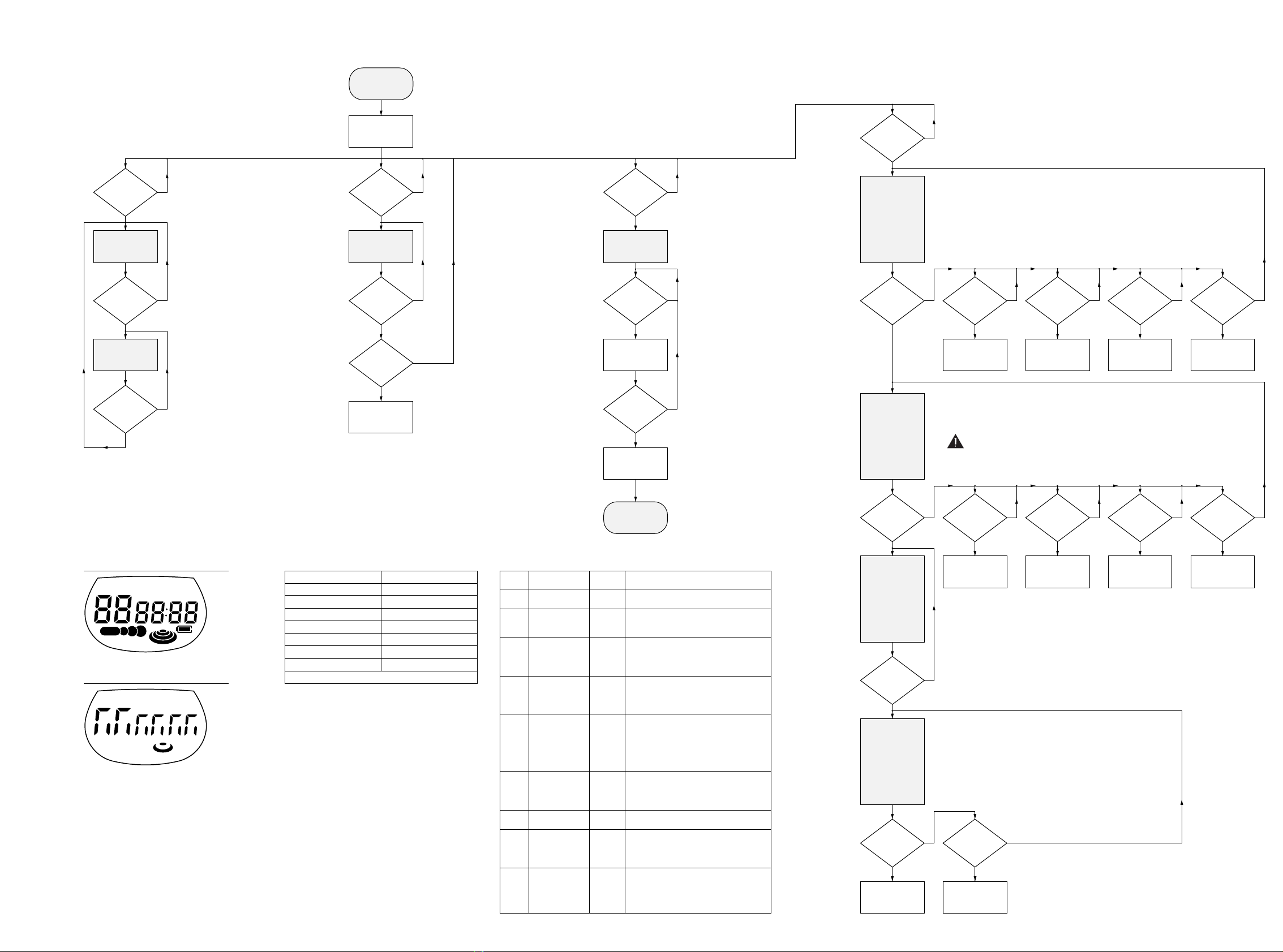
SERVICE TEST PROGRAM
1. PRELIMINARY SETUP
•To enter the service test program hold the keys “MODE” and
“STOP” depressed while turning POWER ON (i.e. connecting
the AC/DC adaptor or inserting batteries).
•The display shows the software version of the built-in
microprocessor (i.e. “S-19”). Versions are counted from “00”
onwards; that means the higher the number the newer the
software.
•The program is now in the main menu – various tests can be
entered by pressing the corresponding buttons (see flow chart
on next page or detailed description of test programs below).
•To exit the service test program disconnect the set from the
power source.
2. DISPLAY TEST
Purpose: Check functionality of display and display driver.
•To enter the display test start service test program and press
the “NEXT” button.
•The display shows test pattern1. All segments are activated for
finding open circuits (see flow chart on next page).
•To jump to the next pattern press the “NEXT” button.
•The display shows test pattern2. All alternate pins (2, 4, ...) are
activated for finding short circuits (see flow chart on next page).
•To jump back to test pattern1 press the “NEXT” button, to exit
the display test and return to the main menu press the “STOP”
button.
3. KEY TEST
Purpose: Check operation of keys.
•To enter the key test start service test program and press the
“MODE” button.
•The display shows “--”.
•Hold key depressed and check corresponding key code on the
display. Key codes can be found in table1 (see flow chart on
next page).
•To exit the key test and return to the main menu press the
“STOP” button.
4. PLAYBACK TEST WITH ERROR ANALYSIS
Purpose: Analyse errors that occur during playback and search
for intermittent failures.
•To enter the playback test start service test program and press
the “DBB” button. Note that the playback test can only be
entered if the CD-door is closed.
•The set now reads the TOC and switches to stand-by.
•Press the “PLAY” button to start the error analysis.
As long as the playback is free of errors the display shows track
and time information like in normal play-mode.
In case of an error a corresponding error code will be displayed.
The meaning of this error code can be found in table2 (see flow
chart on next page).
Note: Errors can either be
“fatal”
or
“non fatal”
. Fatal errors
always stop the playback, non fatal errors only cause a
short interruption of the music. Fatal errors are displayed
as long as the set is connected to the power source, non
fatal errors are displayed until a new error occurs or a
button is pressed.
•To stop the playback test disconnect the set from the power
source.
5. SERVO TEST
Purpose: Check door switch and inner switch, movement of
slide and acceleration of discmotor.
•To enter the servo test start service test program and press the
“PLAY” button.
•The display shows “S
xy
”.
“
x
” indicates state of door switch;
“
y
” indicates state of inner switch.
x,y
= “0” means switch is closed; “1” means switch is open.
•To move slide outside hold the “NEXT” button depressed.
•To move slide inside hold the “PREV” button depressed.
•To accelerate the discmotor clockwise hold the “MODE” button
depressed.
•To accelerate the discmotor counter-clockwise hold the
“PROG” button depressed.
•To enter the focus test press the “PLAY” button, to exit the
servo test and return to the main menu press the “STOP”
button.
6. FOCUS TEST
Purpose: Check movement of lens and operation of focus servo.
•The focus servo loop is switched on and the set starts
searching the focus (“focus ramping”). As soon as the focus
has been found the focus servo loop is closed and the state of
the focus is monitored continuously.
If the focus is OK the display shows “ F”, else “-F”.
•When the disc is turned manually “focus noise” is audible.
•To move slide outside hold the “NEXT” button depressed.
•To move slide inside hold the “PREV” button depressed.
•To accelerate the discmotor clockwise hold the “MODE” button
depressed.
•To accelerate the discmotor counter-clockwise hold the
“PROG” button depressed.
•In case the focus is OK the discmotor test can be entered by
pressing the “PLAY” button, to exit the focus test and return to
the main menu press the “STOP” button.
7. DISCMOTOR TEST
Purpose: Check speed regulation of discmotor.
•The speed regulation is switched on and the discmotor starts
rotating. If the speed reaches 75% of the nom. speed the
display shows “ d”, else “-d”.
•In parallel also the state of the focus is monitored continuously
(display “ F” or “-F”).
•In case the disc speed is OK and the focus is OK the radial test
can be entered by pressing the “PLAY” button, to exit the
discmotor test and return to the main menu press the “STOP”
button.
8. RADIAL TEST
Purpose: Check if radial loop locks and an audio signal is
audible at the headphone output.
•The radial servo loop is switched on, mute is released and the
audio signal is audible. If the system is on track the display
shows “ r”, else “-r”.
•In parallel also the disc speed (display “ d” or “-d”) and the
state of the focus (display “ F” or “-F”) are monitored
continuously.
Note: In case of radial errors the audio output is muted and
muting is not released automatically when the systems
recovers from the error. “-r” remains on the display.
To open mute again press the “NEXT” or “PREV” button.
•To jump 10 tracks outside press the “NEXT” button.
•To jump 10 tracks inside press the “PREV” button.
•To exit the radial test and return to the main menu press the
“STOP” button, to exit the service test program disconnect the
set from the power source.
Important remark:
In radial test mode data to the DRAM is written at 1.2 times the
nominal speed, and read from the DRAM at nominal speed.
Because writing is done faster than reading the DRAM gets full
after a certain time.
In normal play mode the system would now wait until the DRAM
is partly emptied again, jump backwards and resume filling at the
last written position. However, in radial test mode the jumps
would disturb measurements on the radial servo loop.
Therefore this function has been disabled and filling restarts
immediately from the current position of the pick-up unit. As a
result “jumps” are audible during playback.
3-1
CS 46 517

3-23-2
CS 46 518
table1 – key test
DISPLAY OF SET
3
5
6
2
7
8
1
KEYS OF SET
PLAY
NEXT
PREVIOUS
ESA/ESP
MODE
PROGRAM
DBB
Press “STOP” on the CD-player to exit the key test.
PRELIMINARY
SETUP
EXIT
SERVICETEST
PROGRAM
Display shows
software-version
(e.g.“S-19”)
DISPLAYTEST 1
display shows
test pattern1
DISPLAYTEST 2
display shows
test pattern2
KEYTEST
Display shows
“--”
To enter service test program hold “MODE” & “STOP”-button
depressed, while turning POWER ON.
Door switch is ignored →CD-door can be opened.
“STOP”-button pressed in any step returns to main menu.
Remark: Playback test can only
be entered if CD-door
is closed!
CUE-MODE
Track servo jumps
16 tracks forward
“NEXT”
pressed? “MODE”
pressed?
any button
depressed?
“STOP”
button?
“DBB”
pressed?
“PLAY”
pressed?
“PLAY”
pressed?
Error during
playback?
“PLAY”
pressed and
focus OK?
“PLAY”
and focus OK
and speed
OK?
“NEXT”
pressed?
REVIEW-MODE
Track servo jumps
16 tracks backw.
Fatal error?
Display shows
error-code
(see table2)
PLAYBACK
TEST
Slide moves
outside
Slide moves
inside until inner
switch is activated
“NEXT”
depressed?
“NEXT”
pressed?
“NEXT”
pressed?
“PREV”
depressed? “MODE”
depressed? “PROG”
depressed?
Stop playback
check display
according to table1
MAIN MENU
N
Y
N
Y
N
Y
N
Y
N
Y
N
Y
N
Y Y
N
N
Y
N
Y
N
Y
N
Y
N
Y
N
Y
N
Y
Y
N
Y
N
Y
N
Y
Y
N
CODE
E 1000
E 1001
E 1002
E 1003
E 1004
E 1005
E 1006
E 1008
E 1020
ERROR
focus error
radial error
sledge in error
sledge out error
DRAM filling
error
jump error
subcode error
turntable motor
error
focus search
error
TYPE
non fatal
non fatal
non fatal
non fatal
non fatal
non fatal
non fatal
fatal
fatal
CAUSE
Focus point lost for at least 3ms.
CD7 indicates offtrack while radial
tracking is switched on.
The slide did not reach it´s inner pos.
(inner switch of CDM doesn´t close)
within approx.6 seconds.
The slide did not come out of it´s inner
pos.(inner switch of CDM is open)
within approx. 250ms.
The DRAM controller was not able to
connect two consecutive audio frames.
The microcontroller had to perform a
direct audio connection that produces
audible clicks.
The offtrack values of CD7 don´t
decrease properly when jumping tracks,
the jump destination could not be found.
No valid subcode for approx. 230ms.
During start-up, the disc speed did not
reach 75% of the nom. speed within
approx. 6 seconds.
The focus point could not be found
within approx.
10 seconds (no validTOC info), resp.
30 seconds (validTOC info).
table2 – playback error analysis
Disc motor turns
clockwise
(accelerate)
Disc motor turns
counter-clockwise
(brake)
Slide moves
outside Slide moves
inside
“NEXT”
pressed? “PREV”
pressed? “MODE”
pressed? “PROG”
pressed?
N
Y
N
Y
N
Y
N
Y
Disc motor turns
clockwise
(accelerate)
Disc motor turns
counter-clockwise
(brake)
ATTENTION: FROMTHIS TEST ONWARDSTHE
LASER IS SWITCHED ON !!
→AVOID DIRECT EXPOSURETO BEAM !!
ATTENTION: JUMPS ARE AUDIBLE DURING PLAYBACK
(read remark on previous page) !!
RESUME
SHUFFLE REPEATALL
SCAN
PROG
23
DBB 1
REPEATALL
SCAN
test pattern1
test pattern2
“PREV”
pressed?
RADIALTEST
• On track status
“r” = on track
“-r” = not on track
• Disc speed status
“d” = speed OK
“-d” = speed error
• Focus status
“F” = focus OK
“-F” = focus error
DISC MOT.TEST
• Disc speed status
“d” = speed OK
“-d” = speed error
• Focus status
“F” = focus OK
“-F” = focus error
FOCUSTEST
• Focus status
“F” = focus OK
“-F” = focus error
Note: If focus has
been lost, focus
start-up procedure
is entered (ramping).
SERVOTEST
Display shows:
“Sxy”
• State of switches
x = door switch
y = inner switch
“0” = closed
“1” = open
FLOW CHART

3-3 3-3
CS 46 519
SOUND/VOLUME
CONTROL
TC9404FN
DIG. FILTER & DAC
SERIAL
INTERFACE µCON
INTERFACE
TIMING
GEN.
SAA7374GP
CD7 SM5902AF
NPC
TDA1300T
HF-PREAMPLIFIER
L.P.F.
H.P.F.
+
LASER
SUPPLY &
PROTECT.
R2
D1
D2
D3
D4
R1
O5
O1
O3
O4
SCLK
WCLK
MISC
SILD
RAB
SCL
SDA
SBSY
SFSY
SILD, RAB, SCL, SDA
YMLD,YMCLK,YMDATA
ZSENSE, SFSY (PWM_IN)
DATA
ZSCK
ZLRCK
ZSRDATA
BCK
LRCK
DATA
YSCK
YLRCK
YSRDATA
O6
Hf HFIN
RESET
R2
D1
D2
D3
R1
LDonVddl LDON
H=Laser on
MCK
A0...A9, D0...D3
CAS, RAS,WE, OE
MI
+3
DISC
Laser
diode
PHOTO DIODE
ARRAY
TURNTABLE
MOTOR
TRACK
SERVO
FOCUS
SERVO
SLIDE
SERVO
D1 D2
R2R1
D3
VAM2103
CD-DRIVE
Monitor
diode
L.P.F.
L.P.F.
L.P.F.
L.P.F.
L.P.F.
L.P.F.
L.P.F.
L.P.F.
L.P.F.
L.P.F.
L.P.F.L.P.F.
DRAM INTERFACE
A/D-CONVERTER
SHOCK
CONTROL
CONTROLLER
INTERFACE
INPUT
INTERFACE I/O
EXTENSION OUTPUT
INTERFACE
VR
LO
YFLAG
SBSY
YMLD
YMCLK
YMDATA
ZSENSE
RESET
CHGSW
VOUT2
VOUT1
BATM
CHG_ON
(from µP)
POWER
(from µP)
BATIN
DCDTB
SERIAL
INTERFACE
µP
INTERFACE
BS
EMP
SM
LCD
DECODERENCODER
CONTROL PART ATTENUATORINPUT BUFFER
EBU
INTERFACE
RAM
ADDRESS.
SUBCODE
PROCESS.
MOTOR
CONTROL
OUTPUT
STAGES
ERROR
CORRECT.
FRONT END TIMING
DIGITAL PLL
SRAM
EFM
DEMOD.
Vref
KILL
PRE-PROC. FUNCTION
CONTROL
VERSATILE
INTERFACE
AUDIO
PROCESS.
PEAK
DET.
DIGITAL FILTER
ATT CIRCUIT
DE-EMPHASIS FILTER
BA3574BFS
HEADPHONE AMP.
PTMP87CK20F
LCD DRIVER
,
CLOCK GEN.
& TIMING 16bit TIMER
COUNTER ALU
RESET
(FROM DC/DC CONV.)
,,,,,,,,,
,,,,,,,,,
,,,,,,,,,
ROMRAM
4.2MHz
,,,,
,,,,
,,,,
,,,,
,,,,
,,,,
I/O PORTS
Lo
LOLD
VDD
+3
VCC
+A
+A
+µP
SL (PWM signal)
SL FO RA
FO (PWM signal)
RA (PWM signal)
SLIDE_IN
FOCUS_IN
DM±
Sldm±
Focus±
TRACK_IN
VR+3 VG
MPC17A50VM
SERVO DRIVER
SAWTOOTH
OSCILLATOR
LOW VOLTAGE
DETECTOR
DM_IN
VLG VRVG
PWM_DM
(FROM µP)
CL
saw
VG VLG VR
CL
saw
SAW_CLOCK
(FROM DC/DC CONV.)
MUTE_S
(FROM µP)
Track±
L.P.F.
L.P.F.
L.P.F.
RIGHT
LEFT
DC-in socket
+
ACCU or
BATTERY
EXT. DC
DOWN-
CONV.
3.2V
DC/DC
UP-CONV.
ACCU DET.
BATM
SUPPLY/CHARGE CIRCUIT
16.9MHz 4.2MHz 16.9MHz
POWER
NPC_RES
(TO NPC)
CHG_ON
LOBAT
BAT_IN
ACCU_IN
(FROM CHARGE)
PORES
(TO CD7)
MUTE
MUTE_S
KIN1..3, KO1..3
PWM_DM
BEEP
DBB
DBB/LEVEL
(TO SOUND CONT.)
TREB
(TO SOUND CONT.)
NPC_RES
(FROM µP)
TREB (FROM NPC)
DBB/LEVEL (FROM NPC)
DBB (FROM µP)
BEEP (FROM µP)
RESET
PORES
(FROM µP)
RESET
ACCU_IN
(TO µP)
+A +µP+3
FROM/TO DC/DC CONV.
TO SERVO DRIVER
TO SOUND CONT.
DRAM DRAM
1)
,,
,,
CL
saw
VG VLG VR
H-BRIDGE
MOTOR DRIVER 4
H-BRIDGE
MOTOR DRIVER 3
H-BRIDGE
MOTOR DRIVER 1
CL
saw
VG VLG VR
CL
saw
VG VLG VR
H-BRIDGE
MOTOR DRIVER 2
MPC1825AVM
DC/DC CONVERTER
BATTERY CHARGER
STEP-UP
DC/DC CONV.
CHARGE
AMPLIFIER
CHARGE
PUMP
OSC1
OSC2
REGULATOR
CHARGE
PWM2
ERROR AMP
SYSTEM
CONTROL
t
u
r
n
t
a
b
l
e
BEEP
16.9MHz
RO
ANAL.
FILTER
OUTPUT
CIRCUIT
ANAL.
FILTER
OUTPUT
CIRCUIT
MODULATION CIRCUIT
OSC.
KEYBOARD
SAWTOOTH
PWM1
ERROR AMP
LOW BATT DET.
DC-IN DETECT
BANDGAP REF.
SUB REF.
LOW VCPU DET.
DCIN
VG
+µP
TREB
MUTE
DBB
CONT.
RIPPLE
FILTER
TREB
L.P.F.
Vref
1) not on all versions
LOBAT
SAW_CLOCK
(TO SERVO DRIVER)
HEADPHONE
SOCKET
RS
3V
0
-3V
2,5V
0
-2,5V
eye-pattern signal
> 800 mVpp
TB=0.5µs
1
during focus search
TB=0.1s
9
12
10
11
3V
0
servo in or disc motor cw
not moving
servo out or disc motor ccw
servo out or disc motor cw
not moving
servo in or disc motor ccw
16
14
13
15
DATA
WCLK left channel
MSB
LSB
MSB
LSB
right channel
SCLK
TRANSFER OF AUDIO SAMPLESVIA SERIAL INTERFACE OF CD7 AND NPCCD7 →NPC
NPC →DAC
2
3
4
5
6
7
1
14
16
15
13
9
11
1012
BLOCKDIAGRAM MABEL PBAS2

START-UP PROCEDURE
PLAY
pressed ?
µP switches
DC/DC converter on
(POWER=L)
µP resets CD7&NPC
PORES=L
NPC_RES=L
µP initializes CD7
with default
parameter/settings
µP sends
command to CD7:
“move slide inside”
inner switch
closed within
6sec ?
µP sends
command to CD7:
“move slide outside”
µP accelerates
disc motor for
200msec
µP sends
commands to CD7:
“slide servo off”
“focus servo on”
inner switch
open within
0.3sec ?
Start-up procedure for ext.DC supply,
no accu inserted, hold-switch in off pos.,
ESA/ESP off, resume-mode off, CD-door closed.
N
N
N
Y
Y
Y
POWER OFF
(stand-by)
focus
found within
3sec ?
µP accelerates
disc to nom. speed
µP sends
command to CD7:
“switch laser on”
radial&jump
check error ?
release MUTE
µP initializes
radial servo loop
N
Y
Y
Y
subcode check
error ?
Y
N
N
N
PLAY-MODE
subcode check
error handler
radial check
error handler
Y
N
focus search
error handler
retry
focus search ?
display shows
“no disc”
start-up stopped
display shows
“Error”
start-up stopped
disc at nom.
speed within
6sec ?
3-4
CS 46 520

PINNING OF INTEGRATED CIRCUITS
TDA1300T – HF-PREAMPLIFIER AND LASER SUPPLY CIRCUIT (part of CD-drive VAM2103)
Pin Name Direction Description
–––––––––––––––––––––––––––––––––––––––––––––––––––––––––––––––––––––––––––––––––––––––––––––––––––––––––––
1 O4 HF-preamp →CD7 output of current amplifier 4
2 O6 HF-preamp →CD7 output of current amplifier 6
3 O3 HF-preamp →CD7 output of current amplifier 3
4 O1 HF-preamp →CD7 output of current amplifier 1
5 O5 HF-preamp →CD7 output of current amplifier 5
6 O2 HF-preamp →CD7 output of current amplifier 2
7 LDon CD7 →HF-preamp control pin for switching the laser on/off
8 Vddl +3 laser supply voltage
9 Vrfe HF-preamp →equalized output voltage of sum signal of amplifiers 1...4
10 Vrf not connected unequalized output
11 HG GND control pin for gain switch
12 LS CD7 →HF-preamp control pin for double speed switch (switches equalization)
13 C external connection external capacitor (bandwidth of ALPC)
14 Adj →HF-preamp reference input
15 GND GND 0V supply, substrate connection
16 Lo HF-preamp →laser diode current output to laser diode
17 MI monitor diode →HF-preamp laser monitor diode input
18 Vdd +3 positive supply voltage
19 I2 GND photo detector input 2 (not used)
20 I5 diode array →HF-preamp photo detector input 5 (satellite)
21 I1 diode array →HF-preamp photo detector input 1 (central)
22 I3 diode array →HF-preamp photo detector input 3 (central)
23 I6 diode array →HF-preamp photo detector input 6 (satellite)
24 I4 diode array →HF-preamp photo detector input 4 (central)
TC9404FN – Σ-∆MODULATION DAC WITH ANALOG FILTER
Pin Name Direction Description
–––––––––––––––––––––––––––––––––––––––––––––––––––––––––––––––––––––––––––––––––––––––––––––––––––––––––––
1 VDD +3 logic power supply
2 T1 GND test pin
3 P/S +3 parallel control input, serial control switching input
4 VDA +3 analog power supply
5 RO DAC →sound control audio output right channel
6 GNDA GND analog ground
7VR →DAC reference voltage input
8 GNDA GND analog ground
9 LO DAC →sound control audio output left channel
10 VDA +3 analog power supply
11 L/R not connected digital 0 detection output
12 GNDD GND 64fs/256fs/384fs system clock input
13 MCK DAC →master clock output
14 GNDX GND crystal oscillator ground
15 XI →DAC crystal oscillator input
16 XO DAC →crystal oscillator output
17 VDX +3 crystal oscillator power supply
18 BS GND parallel control: de-emphasis filter mode select input
(LATCH) serial control: data latch signal input for ATT;
19 EMP GND parallel control: de-emphasis filter control input
(SHIFT) serial control: shift clock input for ATT;
20 SM GND parallel control: soft mute control input
(ATT) serial control: data input for ATT;
21 HS +3 standard/double speed operation mode switching input
22 DATA NPC →DAC data input
23 BCK NPC →DAC bit clock input
24 LRCK NPC →DAC LR clock input
3-5
CS 46 521

SAA7374 – DECODER AND DIGITAL SERVO IC CD7 (low voltage version)
Pin Name Direction Description
–––––––––––––––––––––––––––––––––––––––––––––––––––––––––––––––––––––––––––––––––––––––––––––––––––––––––––
1 VSSA1 GND supply (analog) of CD7
2 VDDA1 +3 supply (analog) of CD7
3 D1 HF-preamp →CD7 unipolar current input (central diode signal input)
4 D2 HF-preamp →CD7 unipolar current input (central diode signal input)
5 D3 HF-preamp →CD7 unipolar current input (central diode signal input)
6 VRL GND reference input for ADC
7 D4 HF-preamp →CD7 unipolar current input (central diode signal input)
8 R1 HF-preamp →CD7 unipolar current input (satellite diode signal input)
9 R2 HF-preamp →CD7 unipolar current input (satellite diode signal input)
10 IREFT →CD7 current reference for calibration ADC
11 VRH CD7 →reference output from ADC
12 VSSA2 GND supply (analog) of CD7
13 SELPLL +3 selects whether internal clock multiplier PLL is used
14 ISLICE CD7 →current feedback from data slicer
15 HFIN →CD7 comparator signal input
16 VSSA3 GND supply (analog) of CD7
17 HFREF →CD7 comparator common mode input
18 IREF →CD7 reference current pin (nom. VDD/2)
19 VDDA2 +3 supply (analog) of CD7
20 TEST1 GND test control input
21 CRIN µP →CD7 crystal/resonator input
22 CDOUT CD7 →crystal/resonator output
23 TEST2 GND test control input
24 CL16 CD7 →16.9344MHz system clock output
25 CL11 CD7 →11.2896MHz or 5.6448MHz clock output (3-state)
26 RA CD7 →servo driver radial actuator output
27 FO CD7 →servo driver focus actuator output
28 SL CD7 →servo driver slide actuator output
29 TEST3 GND test control input
30 VDD1P +3 supply (digital) of CD7
31 DOBM CD7 →bi-phase mark output (3-state)
32 VSS1 GND supply (digital) of CD7
33 MOTO1 CD7 →motor output1 of CD7; versatile (3-state)
34 MOTO2 CD7 →motor output2 of CD7; versatile (3-state)
35 SBSY CD7 →NPC subcode block sync (3-state)
36 SFSY CD7 →µP subcode frame sync (3-state)
37 RCK →CD7 subcode clock input
38 SUB CD7 →P to W subcode bits (3-state)
39 VSS2 GND supply (digital) of CD7
40 V5 CD7 →versatile output pin of CD7
41 V4 CD7 →HF-preamp versatile output pin of CD7
42 V3 CD7 →NPC versatile output pin of CD7 (open drain)
43 KILL CD7 →kill output; programmable (open drain)
44 MISC CD7 →NPC C2 error flag; output only defined in CD-ROM modes (3-state)
45 DATA CD7 →NPC serial data output (3-state)
46 WCLK CD7 →NPC word clock output (3-state)
47 VDD2P +3 supply (digital) of CD7
48 SCLK CD7 →NPC serial bit clock output (3-state)
49 VSS3 GND supply (digital) of CD7
50 CL4 CD7 →4.2336MHz µP clock output
51 SDA µP ↔CD7 µP interface data I/O line (open drain output)
52 SCL µP →CD7 µP interface clock line
53 RAB µP →CD7 µP interface R/W and load control line
54 SILD µP →CD7 µP interface R/W and load control line
55 NC no connection
56 VSS4 GND supply (digital) of CD7
57 RESET µP →CD7 power-on reset input (active low)
58 STATUS CD7 →µP servo interrupt request line/CD7 status register output (open drain)
59 VDD3C +3 supply core (digital)
60 C2FAIL CD7 →indication of correction failure (open drain)
61 CFLG CD7 →correction flag output (open drain)
62 V1 →CD7 versatile input pin
63 V2 →CD7 versatile input pin
64 LDON CD7 →HF-preamp laser drive on output (open drain)
3-6
CS 46 522

SM5902AF – COMPRESSION-TYPE ANTI-SHOCK MEMORY CONTROLLER NPC
Pin Name Direction Description
–––––––––––––––––––––––––––––––––––––––––––––––––––––––––––––––––––––––––––––––––––––––––––––––––––––––––––
1 VDD +3 supply voltage
2 UC1 DRAM SELECT →NPC µP interface extension I/O line 1
3 UC2 DRAM SELECT →NPC µP interface extension I/O line 2
4 UC3 NPC →SOUND CONTROL µP interface extension I/O line 3
5 UC4 NPC →SOUND CONTROL µP interface extension I/O line 4
6 UC5 INNERSWITCH CDM →NPC µP interface extension I/O line 5
7 DIT NPC →digital audio interface output
8 TEST2 test pin
9 CLK DAC →NPC 16.9344MHz clock input
10 VSS GND ground
11 YSRDATA CD7 →NPC audio serial data input
12 YLRCK CD7 →NPC audio serial L/R clock input
13 YSCK CD7 →NPC audio serial bit clock input
14 ZSCK NPC →DAC audio serial bit clock output
15 ZLRCK NPC →DAC audio serial L/R clock output
16 ZSRDATA NPC →DAC audio serial data output
17 YFLAG CD7 →NPC signal processor IC RAM overflow flag
18 YFCLK GND crystal-controlled frame clock input
19 YBLKCK CD7 →NPC subcode block clock signal output
20 RESET µP →NPC system reset input (active low)
21 ZSENSE NPC →µP µP interface status output
22 VDD2 +3 supply voltage
23 YDMUTE GND forced mute input
24 YMLD µP →NPC µP interface latch clock input
25 YMDATA µP →NPC µP interface serial data input
26 YMCLK µP →NPC µP interface shift clock input
27 OE NPC →DRAM DRAM OE control output (active low)
28 CAS NPC →DRAM DRAM CAS control output (active low)
29 D2 NPC ↔DRAM DRAM data input/output 2
30 D3 NPC ↔DRAM DRAM data input/output 3
31 D0 NPC ↔DRAM DRAM data input/output 0
32 D1 NPC ↔DRAM DRAM data input/output 1
33 WE NPC →DRAM DRAM WE control output (active low)
34 RAS NPC →DRAM DRAM RAS control output (active low)
35 A9 NPC →DRAM DRAM address output 9
36 A8 NPC →DRAM DRAM address output 8
37 A7 NPC →DRAM DRAM address output 7
38 A6 NPC →DRAM DRAM address output 6
39 A5 NPC →DRAM DRAM address output 5
40 A4 NPC →DRAM DRAM address output 4
41 A0 NPC →DRAM DRAM address output 0
42 A1 NPC →DRAM DRAM address output 1
43 A2 NPC →DRAM DRAM address output 2
44 A3 NPC →DRAM DRAM address output 3
3-7
CS 46 523

MPC17A50VM – 4-CHANNEL H-BRIDGE SERVODRIVER
Pin Name Direction Description
–––––––––––––––––––––––––––––––––––––––––––––––––––––––––––––––––––––––––––––––––––––––––––––––––––––––––––
1 CGND GND ground (control part)
2 VLG +3 power supply input (control part)
3 ERR2 CD7 →servo driver error level input (slide error signal)
4 NI2 →servo driver filter capacitor connection in ABS amp circuit section
5 OP2 →servo driver filter capacitor connection in ABS amp circuit section
6 ERR1 CD7 →servo driver error level input (focus error signal)
7 NI1 →servo driver filter capacitor connection in ABS amp circuit section
8 OP1 →servo driver filter capacitor connection in ABS amp circuit section
9 LIM →servo driver limit control level signal input
10 VR →servo driver control reference voltage input (VR=VLG/2)
11 CLK DC/DC converter →servo driver clock signal input
12 OP3 →servo driver filter capacitor connection in ABS amp circuit section
13 NI3 →servo driver filter capacitor connection in ABS amp circuit section
14 ERR3 CD7 →servo driver error level input (track error signal)
15 OP4 →servo driver filter capacitor connection in ABS amp circuit section
16 NI4 →servo driver filter capacitor connection in ABS amp circuit section
17 ERR4 µP →servo driver error level input (disc speed error signal)
18 PHSW GND CH4 mode setup (if PHSW=high, CH4 operates half-bridge)
19 POL not connected CH4 polarity monitor output
20 CFL4 →servo driver pin for connecting filter for capacitor
21 CFL3 →servo driver pin for connecting filter for capacitor
22 OUT4A servo driver →disc motor H-bridge output A
23 OUT4B servo driver →disc motor H-bridge output B
24 VIN34 +A CH3 and CH4 output stage power supply
25 OUT3B servo driver →track actuator H-bridge output B
26 PGND34 GND CH3 and CH4 output stage ground
27 OUT3A servo driver →track actuator H-bridge output A
28 OUT1A servo driver →focus actuator H-bridge output A
29 PGND12 GND CH1 and CH2 output stage ground
30 OUT1B servo driver →focus actuator H-bridge output B
31 VIN12 +A CH1 and CH2 output stage power supply
32 OUT2B servo driver →slide motor H-bridge output B
33 OUT2A servo driver →slide motor H-bridge output A
34 CFL1 →servo driver pin for connecting filter for capacitor
35 CFL2 →servo driver pin for connecting filter for capacitor
36 VG VG power supply input (predriver circuit)
3-8
CS 46 524

MPC1825A – DC/DC CONVERTER AND BATTERY CHARGER
Pin Name Direction Description
–––––––––––––––––––––––––––––––––––––––––––––––––––––––––––––––––––––––––––––––––––––––––––––––––––––––––––
1 DCIN +DC DC power supply input
2RS →DC/DC converter detection input of charge current (battery charger block)
3 RF2 →DC/DC converter connection of error amplifier feedback resistor (battery charger block)
4 INM2 →DC/DC converter inverting input of error amplifier (battery charger block)
5 RF1 DC/DC converter →connection of feedback resistor (switched power supply block)
6 INM1 →DC/DC converter inverting input of error amplifier (switched power supply block)
7 INP1 →DC/DC converter non-inverting input of error amplifier (switched power supply block)
8 DTC →DC/DC converter dead time control input (switched power supply block)
9 VREF DC/DC converter →reference voltage output
10 REFIN →DC/DC converter external reference voltage input
11 BATIN →DC/DC converter input voltage supervises battery cell
12 LOBAT DC/DC converter →µP low volatge detection output
13 CKOUT DC/DC converter →servo driver clock output
14 RSTB DC/DC converter →µP reset signal output
15 SYCSL GND 88.2kHz/176.4kHz mode select input
16 SYNC GND external clock input
17 PCB µP →DC/DC converter system control input
18 CHGON µP →DC/DC converter system control input
19 GND GND ground
20 VCPU DC/DC converter →+µP 3V regulated voltage output
21 VOUT3 not connected DC/DC converter control signal output for system power supply
22 SW +A DC/DC converter driver output for system power supply (open drain)
23 VDO DC/DC converter →DC/DC converter output for system power supply
24 C2L external connection capacitor connection for charge pump
25 C1L external connection capacitor connection for charge pump
26 C1H external connection capacitor connection for charge pump
27 C2H external connection capacitor connection for charge pump
28 VG DC/DC converter →VG charge pump circuit output
29 VOUT1 DC/DC converter →external driver control signal at DC/DC converter
30 VIN →DC/DC converter battery connection (+)
31 DCDTB DC/DC converter →DCIN detection circuit output
32 CHGOUT not connected rechargable battery voltage detection circuit output
33 BATM DC/DC converter →battery (-) battery connection (-)
34 CHGFIL external connection external filter capacitor connection for battery charger voltage detection
35 VOUT2 DC/DC converter →external driver control signal (battery charger voltage block)
36 CHGSW DC/DC converter →battery charger switch control output
3-9
CS 46 525

4-14-1
CS 46 526
L= WEAK, H= EMPTY
3.2V - DC/DC - UP-CONVERTEREXT. DC-DOWNCONVERTER
switch
Inner-
motor
motor
Slide-
Disc-
from/to signal processing part from/to signal processing part from/to control part
NI-CAD-ACCU
POWER
CHG_ON
SAW_CLOCK
ACCU_IN
RESET
PWM_DM
LOBAT
BATIN
DCDTB
SUPPLY/SERVODRIVER PART
7956 K13
7956 I12
7952 H14
7951 M12
7950 M12
7264 F11
7259 H 9
7255 E 3
7254 G10
7253 F 8
7252 D10
7251 C 6
6257X I10
6256 H10
6255 B 2
6254 C 2
6252 I 7
6250 A 2
5252 C10
5251 I 8
3969 J14
3968 L13
3967 M13
3966 J13
3961 J12
3958 H18
3957 K13
3956 J13
3955 K12
3954 K12
3953 M13
3952 M12
3951 L11
3950 M11
3299 K 2
3297 G 9
3283 I 9
3282 I 9
3271 H 2
3270 E11
3269 D11
3268 C11
3267 C10
3266 E 7
3265 G 8
3263 D11
3261 D 6
3260 K 3
3259 H 2
3258 H 2
3257 I 1
3256 H 1
3255 I 1
3254 G 3
3253 F 3
3252 G 2
3251 F 2
3243 F11
3242 F10
3241 F10
3240 E 6
2971 L18
2970 J18
2963 H18
2962 M18
2961 M18
2960 L18
2958 I18
2957 H18
2956 M14
2955 L14
2954 J14
2953 I14
2952 M13
2951 M12
2950 K12
2280 H 7
2279 J 2
2278 H 3
2277 D10
2275 B 3
2274 C10
2270 D 6
2269 E11
2268 E11
2265 C 9
2264 C 9
2263 E 8
2262 H 7
2261 J 7
2260 J 6
2259 H 7
2258 H 6
2257 F 6
2255 H 2
2254 G 2
2253 F 2
2252 F 2
2250 B 1
1951 L21
1950 I20
1250 B 2
45617 8 9 101112131415162 17 18 19 20 213
K
J
I
N
H
G
F
E
D
C
B
A
M
L
K
J
I
N
H
G
F
E
D
C
B
A
M
L
45617 8 9 101112131415162 17 18 19 20 213
6250
SB10-05PCP
6252
SB10-05
6254
SB10-05PCP
6256
BAT254
6257X
BAT54
uP
uP
ESD
A
SD SD SD
SD SD
3271
1M
3263
47k
3k9
3966
3k9
3967
3950
0R05
3951
10k
3958
1k
3253
1M
3251
4k7
3254
1M
3252
4k7
3261
120R
3265
4R7
3266
390R
3256
270k%
3257
220k%
3259
470k
3258
100k
3270
1k8% 3269
8k2% 3268
680R
3267
10R
3955
47k% 3954
47k%
3957
47k 3956
10k
3255
680k
10k
3953
3k3
3952
3297
2R2
3241
10k
3242
470k
3243
22k
3240
120R
3260
10k
3299
1k
3283
22k
3282
22k
5k6
3968
4k7
3969
2k2
3961
+A
+A
+A
+A
+3 +3
VG VG
+uP
+3
+3
+3
+3
+3
+uP
+A
7951
BC857B
7251
2SB1123
7259
BC857B
7254
BUK581
2280
1u
2254
470n
2275
100n
2265
100n
470p
2953
470p
2954
470p
2955
470p
2956
470p
2957
470p
2958
470p
2961
470p
2962
1n
2252
1n
2253
2258
100n
2259
100n
2262
100n
2257
10n
2255
1u
2274
22n
2269
1u
100n
2263
2250
100n
100n
2950
2952
10n
100n
2951
1u
2971
330n
2970
2277
330p
2279
100n
2278
33n
1u
2963
2270
330n
5252
20u
7950
BC847B
7253
2SD1623T
7252
2SD1623T
7264
BC847B
100u
2268
100u
2264
2960
100u
22u
2261
22u
2260
6255
BAS216
7
5
6
47956
LM2904N
2
31
8LM2904N
7956
1950
2
1
1951
1
2
3
4
PWM_DM
DCDTB
ACCU_IN
CHG_ON
FOCUS_IN
TRACK_IN
INNERSW
SLIDE_IN
FOCUS+
FOCUS-
TRACK+
TRACK-
BATIN
POWER
LOBAT
RESET
M
M
2 x LR6
7952
10
11
12
13
14
15
16
17
18 19
1
20
21
22
23
24
25
26
27
28
29
2
30
31
32
33
34
35
36
3
4
5
6
7
8
9
PSB
SAWTOOH
VLG
ERR3
NI3
OP3
OP1
NI1
ERR1
OP2
NI2
ERR2
PHSW
ERR4
NI4
OP4
VG
VG
OUT3A
OUT2A
OUT4A
OUT3B
OUT2B
OUT4B
OUT1A
VLG
VLG
OUT1B
CFL2
CFL4
CFL3
CFL1
POL
VG
GEN.
SAW.
LOW VOLTAGE
CLK
VR
LIM
OP1
NI1
ERR1
OP2
NI2
ERR2
VLG
CGND
PHSW
ERR4
NI4
OP4
ERR3
NI3
OP3
DETECTOR
VR
VR
VR
VR
DRIVER
MOTOR
DRIVER
MOTOR
DRIVER
MOTOR
DRIVER
MOTOR
CH3
CH1
CH2
CH4
PGND34
PGND12
OUT3A
OUT2A
OUT4A
OUT1A
OUT2B
OUT4B
OUT3B
OUT1B
VIN34
VIN12
CFL4
CFL3
CFL2
CFL1
POL
VG
MPC17A50VM
7255
10
11
12
13
14
15
16
17
18 19
1
20
21
22
23
24
25
26
27
28
29
2
30
31
32
33
34
35
36
3
4
5
6
7
8
9
BANDGAP
REF.
REFIN
CONTROL
SYSTEM
BATIN
VREF
DTC
INP1
INM1
RF1
INM2
RF2
RS
CHGON
PCB
SYNC
SYCSL
RSTB
CKOUT
LOBAT
DCIN
+
-
-
+
-
+
SUB
REF.
OSC 2
CONTR.
CHARGE
SAWTOOTH
-
+
DETECT
DCIN
+
-
OSC 1
+
-
CHARGE
PUMP
+
-
-
+
CHGSW
CHGFIL
DCDTB
VOUT2
VOUT3
VOUT1
BATM
VCPU
OUT
CHG
GND
VDO
C2H
C2L
C1H
SW
C1L
VIN
VG
MPC1825AVM
1250
HEC3600
5251
100u
MUTE_S
MUTE_S
MABEL 3A/4A - PB2 Supply/Servodriver Part 19980318
4.1V
4.1V
0.1V
0.1V
0V
0.3V
0.3V
0.1V
0V
0V
0.4V
0.4V
0.4V
0.5V
0.7V
0.7V
0.8V
0.9V
3.0V
3.0V
3.0V
3.0V
3.5V
1.3V
4.3V
0V
0V
0V
4.1V
3.8V
1.9V
1.9V
5.6V
9.8V
4.2V
0V
0V
11.8V
4.1V
4.1V
3.1V
2.9V
3.9V
4.6V
4.6V5.0V
0V 0V
0.5V
10.5V
0V
0.1V
0.1V
0.2V
0.5V
0.4V
0V
0V
0V
0V
0V
4.1V
4.1V
3.1V
3.1V
1.6V
1.6V
1.6V
2.2V
0.7V
0.7V
0.7V
1.9V
3.1V
1.7V
1.9V
3.1V
1.5V
1.5V
2.6V
2.0V
1.2V
1.5V
0.7V
1.5V
2.0V
0V
DC Voltages measured in
PLAY-mode, ESA off
Set supplied via mains adapter
4.1V
12
10
9
11
16
EVM
V
170 KHz
3V
0
-3V
2,5V
0
-2,5V
during focus search
TB=0.1s
9
12
10
11
servo in or disc motor cw
not moving
servo out or disc motor ccw
3V
0
servo out or disc motor cw
not moving
servo in or disc motor ccw
16
14
13
15

4-2 4-2
CS 46 527
H=5902
L=5859
NPC SEL
8M
4M
DRAM
size 3845C,3842H
3844K,3843G
Stuff
Hf
CL4
NPC_RES A9
A9
A9
DD2
DD2 DD2
DD3
DD3 DD3
WE
WE WE
RAS
RAS RAS
A4
A4 A4
PWM_IN
A8
A8 A8
A7
A7 A7
A6
A6 A6
A5
A5 A5
DD1
DD1
DD1
DD0
DD0
DD0
SEL1
SEL2
WCLK
WCLK
YFLAG
YFLAG
YMCLK
YMDATA
YMLD
ZSENSE
SBSY
SBSY
A0
A0
A1
A1
A2
A2
A3
A3
DATA
DATA
SCLK
CL4
SCLK
to supply/servo-driver part
A10
VDD2
to audio part
GND
VDD
D4
D5
D3
D2
D1
LDON
VDDL
RFE
LS
GND
TRACK+
FOCUS+
FOCUS-
TRACK-
SIGNAL PROCESSING PART
3x
220p
3x
220p
A3
A2
A1
A0
LO
LD
16.9 MHz
451 6 7 8 9 10 11 12 13 14 152 16 17 18 19 20 21 223
J
I
H
G
M
F
E
D
C
B
A
L
K
J
I
H
G
M
F
E
D
C
B
A
L
K
451 6 7 8 9 10 11 12 13 14 152 16 17 18 19 20 21 223
D
SD
SD
D
D
D
DD
D
D
D
D
M
M
SD
SD
SD
HF
HF
SDSDSD
DADA
HF
HF
HF
HF
DA DA
DA DA DA
DADA
HF
HF
SD SD
SD
SD SD
D
M
MDA
SD
M
uP
+3
+3
+3
+3
+3
+3
+3
+3+3
+3
+3
+3
+3
+3
100N
2853L
100n
2831
33n
2836
2837
33n
100n
2833
2830
100n
100n
2832
2818
2817
2816
2821
2820
2819
82p
2815X
10n
2822
47p
2823
22n
2824
2829
2n2
2809
3n3
1n5
2806
3n3
2808
3n3
2807
3n3
2810
2814
1n5
2813
560p
2827
33n
2834K
33n
2835J
33n
1n5
2811
100R
3853L
47k
3870L
0R05
3871M
22k
3857
22k
3856
22k
3821
22k
3819
22k
3820
22k
3818
22k
3817
10k
3837
1k
3849
1k
3848
1k
3847
4R7
3841
3838
22R
3823
10k
3828
10k
3827
10k
3826
10k
3825
10k
3824
10k
270k
3829
10R
3822 4R7
3834
4k7
3830
2k2
3813
3809
2k2
3811
2k2 2k2
3812
2k2
3810
2k2
3814
4R7
3836
100R
3846
10k
3844K
10k
3842H
0R05
3843G
0R05
3845C
3839
22k
4R7
3832
22k
3831
3850K
4R7
3851J
4R7
3833
100k
3858
1M
3859
10R
7810J HYB314400BJ-60
13 14
15
16
17
18
22
23
24
25
126
2
3
4
5
9
10
11
12 A2
A0
A1
VCC
A3
A9
RAS
WE
I/O2
I/O1
CAS
I/O3
I/O4
GND
OE
A6
A4
A5
A8
A7
4M BIT (1M x 4) DRAM
7811K HYB314400BJ-60
13 14
15
16
17
18
22
23
24
25
126
2
3
4
5
9
10
11
12
A2
A0
A1
VCC
A3
A9
RAS
WE
I/O2
I/O1
CAS
I/O3
I/O4
GND
OE
A6
A4
A5
A8
A7
4M BIT (1M x 4) DRAM
consig
1800
10
11
12
13
14
15
16
17
18
1
2
3
4
5
6
7
8
9
22u
2812
2826
22u
2825
22u
2843
22u
NPC_RES
TRACK+
FOCUS+
FOCUS-
TRACK-
TREB
DBB/LEVEL
CL4
CLK
LRCLK
SRDA
SLIDE_IN
TRACK_IN
FOCUS_IN
SILD
RA
PORES
SDA
SCL
STATUS
ZSENSE
YMLD
YMDATA
YMCLK
CL16
INNERSW
PWM_IN
SAA7374GP
7807
10
11
12
13
14
15
16
17 18 19
1
20 21 22 23 24 25 26 27 28 29
2
30 31 32
33
34
35
36
37
38
39
3
40
41
42
43
44
45
46
47
48
49
4
50515253545556575859
5
6061626364
6
7
8
9
PINS
MICROPROCESSOR
V1...VV5
INTERFACE
DETECT
PEAK
KILL
MOTO2
MOTO1
WCLK
VDD2P
SCLK
SBSY
SFSY
VSS2
MISC
DATA
RCK
SUB
KILL
V5
V4
V3
VSSA1
VSSA3
SELPLL
HFIN
Vref
D3
D2
D1
VSSA2
VRH
IREFT
R2
R1
D4
VRL
VDDA1
ISLICE
DIGITAL
DEMOD.
CORRECTION
ERROR
PROC.
PRE-
EFM
PLL
CONTROL PART
CONTROL
FUNCTION
SRAM
FLAGS
TIMING
CONTROL
MOTOR
INT.
EBU
ADDR.
RAM
VERSATILE
OUTPUT
STAGES
FO SILD
SL RAB
TEST3 SCL
SERIAL DATAAUDIO
VDD1P
LDON
INTERFACEPROCESSOR SDA
DOBM SUBCODE CL4PROCESSOR
VSS1
VSS3
ADC
IREF FRONT END V2
VDDA2 V1
TEST1 CFLG
CRIN C2FAIL
CROUT VDD3C
TEST2 STATUS
CL16 RESET
CL11
HFREF
VSS4
RA NC
7809
SM5902
10
11
12 13 14 15 16 17 18 19
1
20 21 22
23
24
25
26
27
28
29
2
30
31
32
33
343536373839
3
4041424344
4
5
6
7
8
9
VSS
CLK
TEST2
TEST1
UC5
UC4
UC3
UC2
UC1
VDD
YSRDATA
INPUT
INTERFACE
BUFFER
ENCODER
INPUT
DRAM INTERFACE
CONTROL
SHOCK
ATTENUATOR
INTERFACE
DECODER
OUTPUT
OE
CAS
D2
D3
DO
D1
WE
YMDATA
YMCLK
YMLD
YDEMUTE
YSCK
ZSCK
ZLRCK
ZSRDATA
YFLAG
YFCLK
YBLKCK
YLRCK CONTROL I/O EXTENSION
RESET
ZSENSE
CONTROLLER I/F
A2
A1
A0
A4
A5
A6
A3
A7
A8
A9
RAS
to supply/servo-driver part
from/to Control part
MABEL 3A/4A - PB2 Signal Processing Part 19980318
ITEMNUMBER EXTENSIONS
C,G,H,J,K = DRAM size selection
L = SM5902 version of NPC
M = SM5859 version of NPC
X = component only forseen (not in use)
% = tolerance of resistor is 1%
to/from CD-Drive
VAM2103
15 13 14
1
3
2
4
6 5 7
H = Laser on
DC Voltages measured in
PLAY-mode, ESA off
Set supplied via mains adapter
PDM output
ESA on 4.2MHz
ESA off 2.1MHz
3.0V
3.0V
3.0V
3,0V
3,0V
3,0V
3,0V
1,5V
1,5V
1,5V
0V
0V
0V
0V
0V
0V
3,0V
3,0V
3,0V
0V
0V
1,5V
1,5V
0,2V
0V
0V
0V
2,0V
3,0V
0,1V
1,8V
2,0V
1,0V
1,5V
1,5V
1,5V
1,5V
1,5V
1,5V
1,4V
1,4V
3,0V
1.6V
1.6V
1.2V
0V
0V
0V
0V
0V
0V
1,5V
3,0V
3,0V
0V
0V
0V
0V
0V
3.0V
3.0V
2.8V
2.4V
0.2V
1.6V
3,0V
3,0V
EVM
V
eye-pattern signal
> 800 mVpp
TB=0.5µs
1
3V
0
servo out or disc motor cw
not moving
servo in or disc motor ccw
16
14
13
15
DATA
WCLK left channel
MSB
LSB
MSB
LSB
right channel
SCLK
TRANSFER OF AUDIO SAMPLESVIA SERIAL INTERFACE OF CD7 AND NPCCD7 →NPC
NPC →DAC
2
3
4
5
6
7
1800 H 1
2806 K 5
2807 K 5
2808 L 4
2809 L 5
2810 L 5
2811 L 4
2812 C 7
2813 H 7
2814 H 7
2815X J 7
2816 F 8
2817 F 8
2818 F 9
2819 G 8
2820 G 8
2821 G 9
2822 I 8
2823 J 9
2824 J 9
2825 K10
2826 D 8
2827 D9
2829 J 8
2830 D14
2831 D15
2832 J14
2833 H17
2834K B18
2835J E18
2836 I20
2837 C12
2843 G 2
2853L I21
3809 K 5
3810 K 6
3811 K 4
3812 K 5
3813 L 5
3814 L 5
3817 A 8
3818 A 8
3819 A 8
3820 A 8
3821 A 9
3822 C 8
3823 E 8
3824 F 8
3825 F 8
3826 F 8
3827 G 8
3828 G 8
3829 G 9
3830 J 7
3831 I 8
3832 J10
3833 J10
3834 C 9
3836 C14
3837 A 9
3838 E15
3839 F15
3841 J14
3842H F17
3843G F17
3844K F17
3845C F17
3846 F17
3847 J19
3848 J19
3849 J19
3850K B18
3851J E18
3853L I21
3856 D 9
3857 B12
3858 J11
3859 G 3
3870L C11
3871M D10
7807 E12
7809 E18
7810J D21
7811K B21

4-3
CS 46 528
RESUME
SHUFFLE REPEATALL
SCAN
PROG
23
DBB 1
KO3
ESD
TO/FROM CONTROL PART / 1401
KO2KO1KIN3KIN2KIN1
MEMBRANE ASSEMBLY 4822 360 10363
1001
NEXT
PREV
STOP
MODE
PROG
DBB
ESA PLAY
1002 1003
1006 1005
1007 1008
1004

4-44-4
CS 46 529
from/to signal processing part from/to audio part
from/to supply/servodriver part
C0
C2
S1
S2
S5
S9
S10
S11
S12
C1
C3
KIN1
KIN1
KIN1
KIN2
KIN2
KIN2
KIN2
KIN3
KIN3
KIN3
KIN3
KIN3
KO3
KO3
KO3
KO2
KO2
KO1
KO1
HOLD
HOLD
BATIN
CHG_ON
NPC_RES
RESET
S13
S
ZSENSE
DCDTB
DCDTB
ACCU_IN
YMLD
RESUME
RESUME
PWM_DM
POWER
LOBAT
S0
S3
S4
S6
S7
S8
PWM_IN
YMCLK
YMDATA
CONTROL PART
Start-up circuit
7405 G 5
7404 G 4
7400 C 8
5400 E 7
3432 F12
3431 F12
3430 F 7
3425 G 4
3424 G 5
3423 F 4
3421 G 3
3420 E 5
3417 H 3
3405 A 4
3404 A 3
3403 B11
3402 B11
3401 B11
3377 H12
3376 H12
2413 E 5
2412X E 7
2411 E 7
2410 F 6
2407 H11
2405 G 3
2404 G 2
1430 A 5
1418 A 2
1401 A 6
45617 8 9 10 11 12 1323
F
E
D
C
I
B
A
H
G
F
E
D
C
I
B
A
H
G
45617 8 9 10 11 12 1323
+uP
+uP +uP
+uP
+uP
+uP
+uP
uP
uPuP
uP
uP
ESD
uP
uP
uP
uP
uP
D
uP
uP
3376
1M
3377
1M
3417
1M
3425
1M
3421
1M
3423
1M
3424
47k
3432
100
3431
100
1k
3430
3404
220k
3405
220k
3401
220k
3402
220k
3403
220k
10k
3420
7404
BC847B
NPC_RES
2405
1n
2404
1n
100n
2407
1n
2410
22p
2412X
22p
2411
22n
2413
1401
10
11
12
13
14
15
16
17
18
19
1
20
21
22
23
24
25
26
2
3
4
5
6
7
8
9
RESET
MUTE_S
DCDTB
CL4
MUTE_S
ZSENSE
PWM_IN
YMLD
YMDATA
YMCLK
SDA
SCL
RA
SILD
PORES
STATUS
DBB
CHG_ON
ACCU_IN
MUTE
BATIN
POWER
LOBAT
PWM_DM
BEEP
SSSS2-131418
1234
BC857B
7405
1430
ESE11SH1
DOOR
7400
TMP87CH20F
8
7
6
5
25 26 27 28 29 30 31 32 34 35 36 37 38 39 40
41
16
10
11
17
18
19
20
21
22
23
24
42
43
44
45
46
47
48
49
50
51
12
4
74 73 72 71 70 69 68 67 66 65
3
64
63
62
61
60
59
58
57
56
55
2
54
53
1
80 79 78 77 76 75
52
33
9
15
13
14 TEST
VLC
I/O PORT P0
LCD - DRIVER
VDD
RESET
16 BIT
TIMER
WATCHDOG
TIMER/COUNTER
RAM
ROM
I/O PORT P1
VSS
CLOCK
I/O PORT P4 I/O P5
I/O PORT P3 P2 I/O P2
8 BIT CPU
5400
4.23
Resume/Hold
MABEL3A/4A - PB2 Control Part 19980318
from/to membrane assembly
16
0V
DC Voltages measured in PLAY-mode, ESA off
Set supplied via mains adapter
0V
0.2V
0.2V
2.0V
2.0V
3.0V
3.0V
0.7V
2.6V
1.8V
3.0V
3.0V
0V
3.0V
3.0V
2.4V
2.5V
2.2V
0V
0V
0V
0.3V
0.3V
0.3V
3.0V
3.0V
3.0V
3.0V
2.9V
2.8V
1.5V
3.0V
0V
3.2V
3.0V
3.0V
1.8V
1.5V
1.5V
1.5V
1.5V
3.0V
2.5V
0V
2.5V
3.0V
EVM
V
SERVICE TEST
TB 5ms/Div
Pin 6
COM 3
3.8V
3.8V
TB 5ms/Div
Other manuals for AZ7381
2
This manual suits for next models
9
Table of contents
Other Philips Portable CD Player manuals