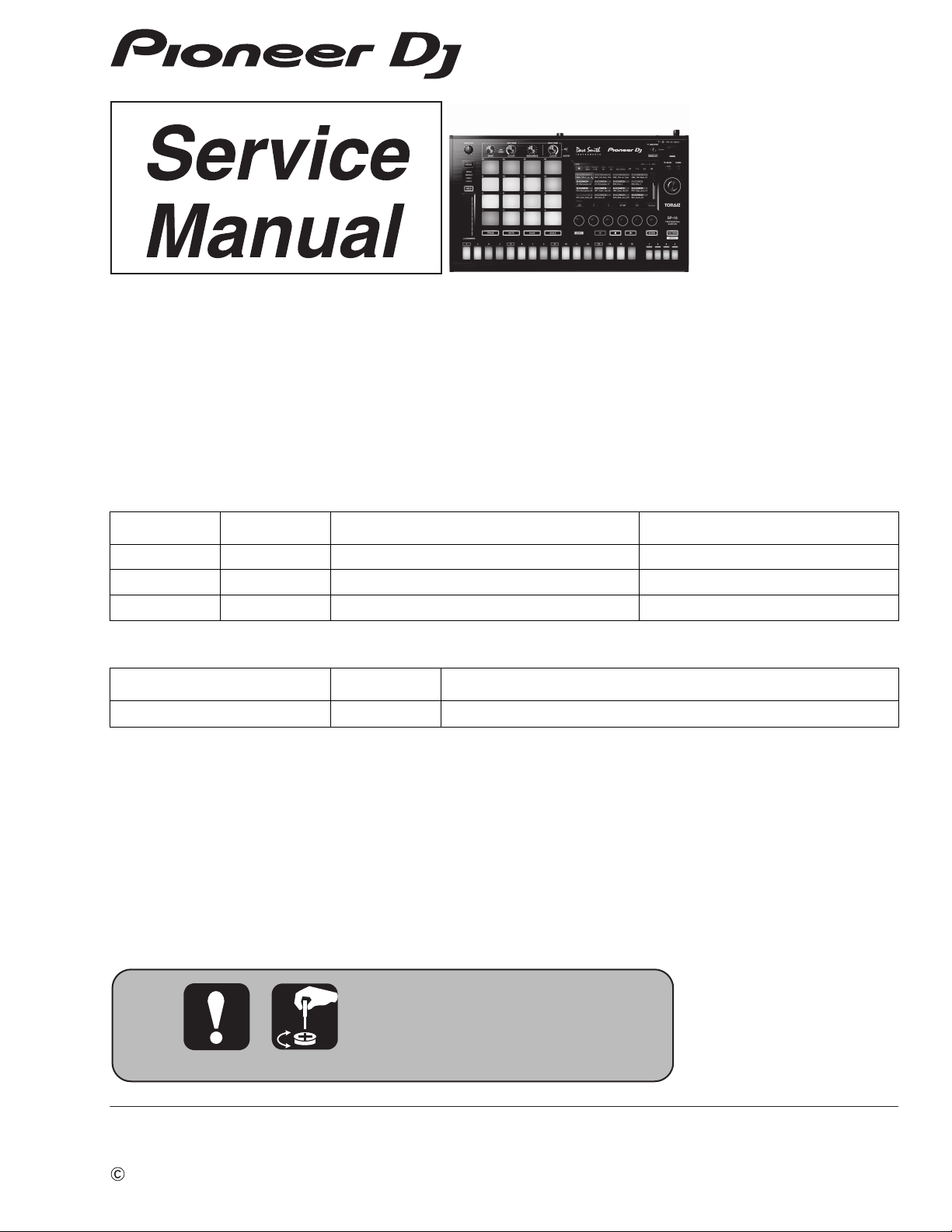
PIONEER DJ TSP-16 User manual

ORDER NO.
Pioneer DJ Corporation 6F, Yokohama i-Mark Place, 4-4-5 Minatomirai, Nishi-ku, Yokohama, Kanagawa 220-0012 Japan
2016 Pioneer DJ Corporation
TSP-16
QRT1001
PROFESSIONAL SAMPLER
TSP-16
THIS MANUAL IS APPLICABLE TO THE FOLLOWING MODEL(S) AND TYPE(S).
THIS SERVICE MANUAL SHOULD BE USED TOGETHER WITH THE FOLLOWING MANUAL(S).
Model Type Power Requirement Remarks
TSP-16 SYXJ AC 100 V to 240 V
TSP-16 UXJCB AC 100 V to 240 V
TSP-16 AXJ AC 100 V to 240 V
Model Order No. Remarks
TSP-16 QRT1002 SCHEMATIC DIAGRAM, PCB CONNECTION DIAGRAM, PCB PARTS LIST

2TSP-16
12 3 4
A
B
C
D
E
F
12 3 4
SAFETY INFORMATION
WARNING
This product may contain a chemical known to the State of California to cause cancer, or birth defects or other reproductive
harm.
Health & Safety Code Section 25249.6 - Proposition 65
This service manual is intended for qualified service technicians; it is not meant for the casual do-it-
yourselfer. Qualified technicians have the necessary test equipment and tools, and have been trained
to properly and safely repair complex products such as those covered by this manual.
Improperly performed repairs can adversely affect the safety and reliability of the product and may
void the warranty. If you are not qualified to perform the repair of this product properly and safely, you
should not risk trying to do so and refer the repair to a qualified service technician.

3
TSP-16
56 7 8
56 7 8
A
B
C
D
E
F
CONTENTS
SAFETY INFORMATION.......................................................................................................................................................... 2
1. SERVICE PRECAUTIONS .................................................................................................................................................... 4
1.1 NOTES ON SOLDERING ............................................................................................................................................... 4
1.2 NOTES ON REPLACING ............................................................................................................................................... 4
1.3 SERVICE NOTICE.......................................................................................................................................................... 4
2. SPECIFICATIONS................................................................................................................................................................. 5
2.1 ACCESORIES ................................................................................................................................................................ 5
2.2 SPECIFICATIONS .......................................................................................................................................................... 5
3. BASIC ITEMS FOR SERVICE .............................................................................................................................................. 6
3.1 CHECK POINTS AFTER SERVICING ........................................................................................................................... 6
3.2 JIGS LIST ....................................................................................................................................................................... 6
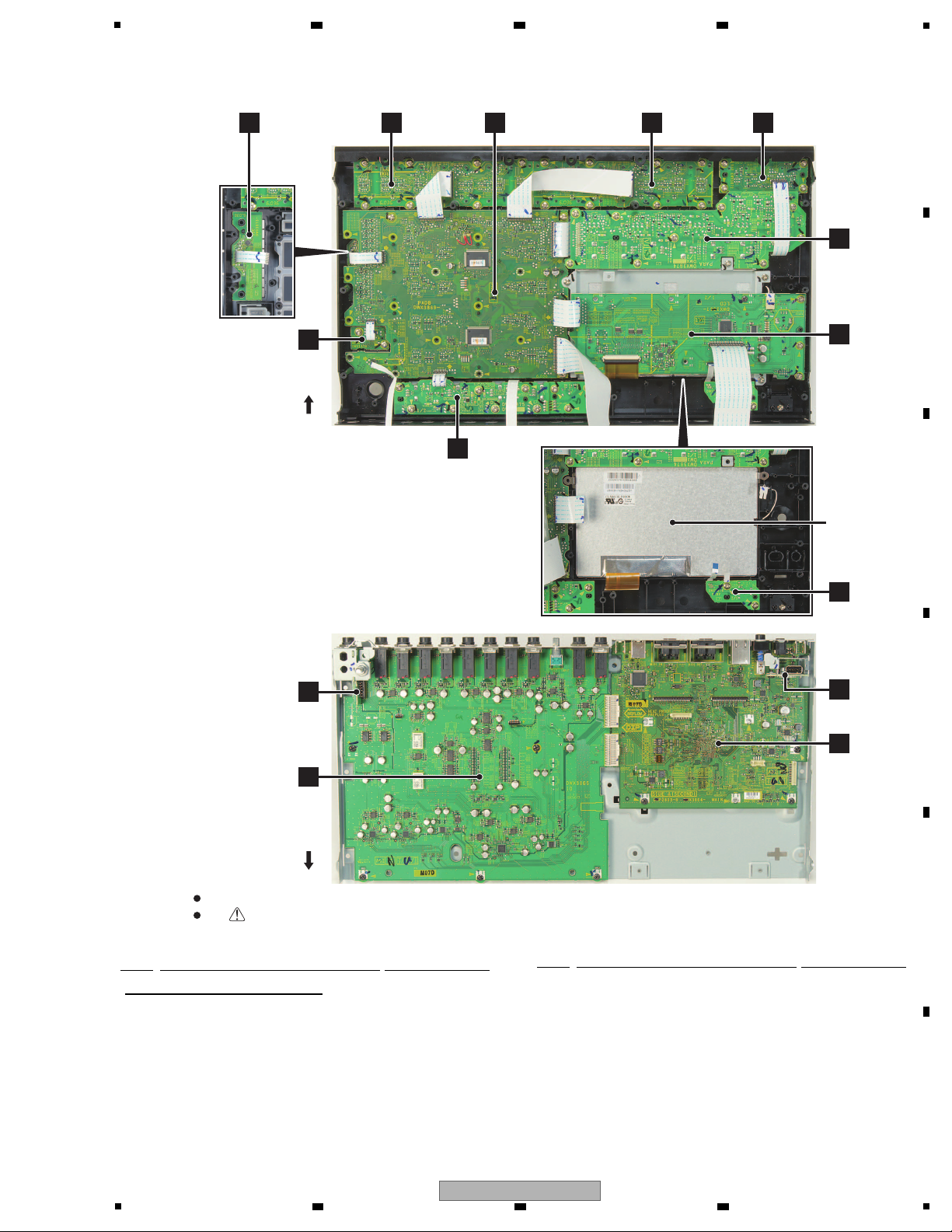
3.3 PCB LOCATIONS ........................................................................................................................................................... 7
4. BLOCK DIAGRAM ................................................................................................................................................................ 8
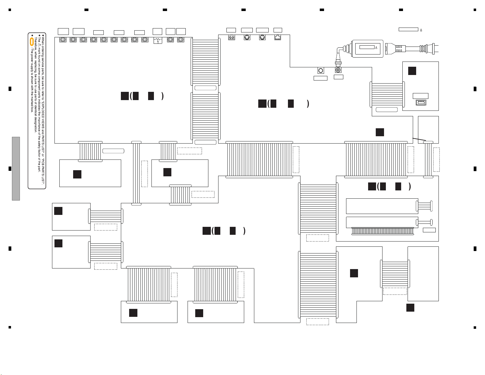
4.1 OVERALL WIRING DIAGRAM ....................................................................................................................................... 8
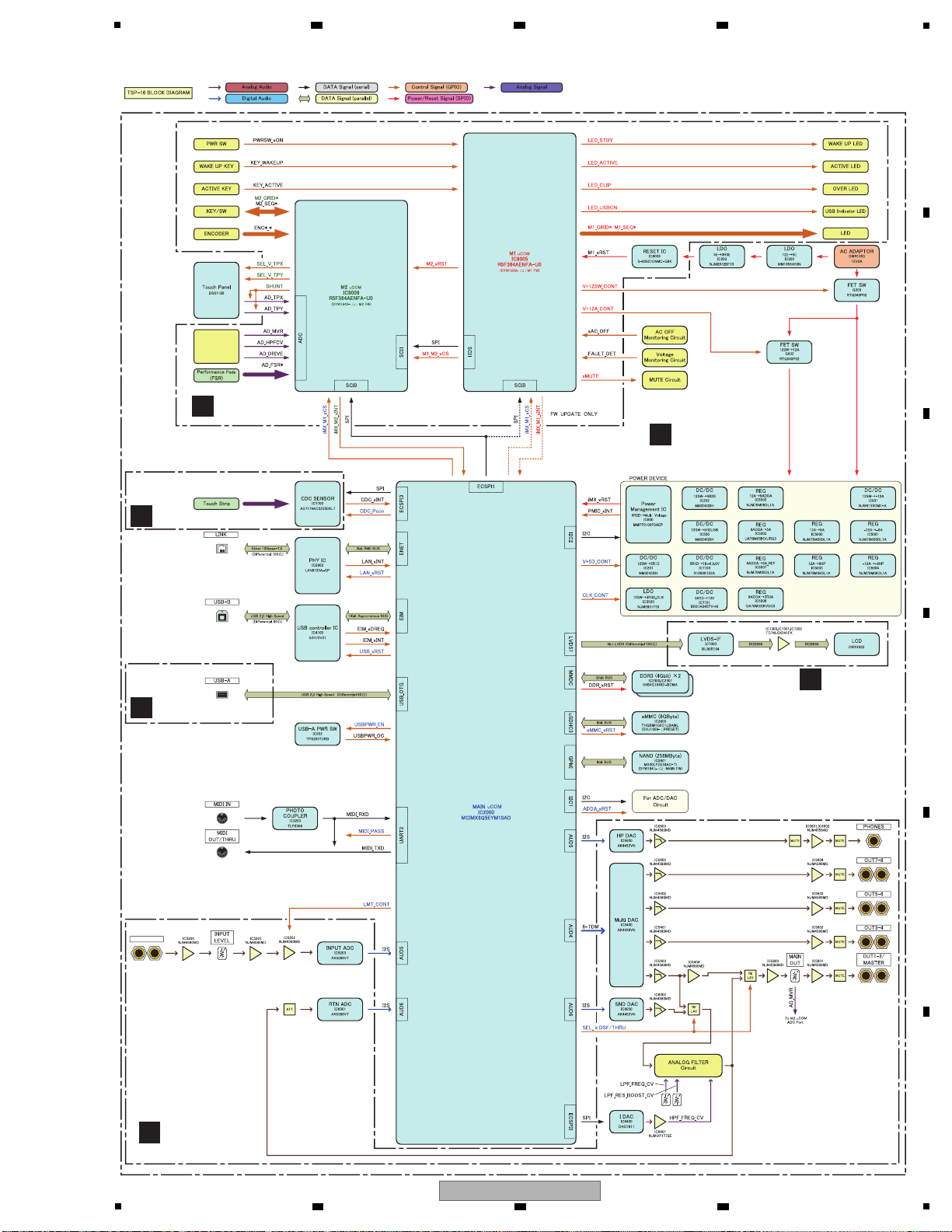
4.2 SIGNAL BLOCK DIAGRAM............................................................................................................................................ 9
4.3 POWER BLOCK DIAGRAM ......................................................................................................................................... 10
4.4 MATRIX TABLE............................................................................................................................................................. 11
5. DIAGNOSIS ........................................................................................................................................................................ 15
5.1 STARTUP SEQUENCE ................................................................................................................................................ 15
5.2 TROUBLESHOOTING.................................................................................................................................................. 16
Starting Trouble.......................................................................................................................................................... 16
Display Trouble .......................................................................................................................................................... 17
Operation Trouble ...................................................................................................................................................... 18
Audio Trouble ............................................................................................................................................................. 19
Interface Trouble ........................................................................................................................................................ 22
Other Trouble ............................................................................................................................................................. 23
5.3 VOLTAGE MONITORING CIRCUIT .............................................................................................................................. 24
5.4 PIN ASSIGNMENT LIST .............................................................................................................................................. 25
6. SERVICE MODE ................................................................................................................................................................. 39
6.1 TEST MODE................................................................................................................................................................. 39
6.2 ABOUT THE DEVICE................................................................................................................................................... 46
7. DISASSEMBLY ................................................................................................................................................................... 47
8. EACH SETTING AND ADJUSTMENT ................................................................................................................................ 57
8.1 NECESSARY ITEMS TO BE NOTED........................................................................................................................... 57
8.2 UPDATING OF THE FIRMWARE ................................................................................................................................. 58
9. EXPLODED VIEWS AND PARTS LIST............................................................................................................................... 59
9.1 PACKING SECTION ..................................................................................................................................................... 59
9.2 EXTERIOR SECTION .................................................................................................................................................. 61
9.3 PANEL SECTION (1/2) ................................................................................................................................................. 63
9.4 PANEL SECTION (2/2) ................................................................................................................................................. 65
9.5 CHASSIS SECTION ..................................................................................................................................................... 67

4TSP-16
12 3 4
A
B
C
D
E
F
12 3 4
1. SERVICE PRECAUTIONS
1.1 NOTES ON SOLDERING
1.2 NOTES ON REPLACING
1.3 SERVICE NOTICE
• For environmental protection, lead-free solder is used on the printed circuit boards mounted in this unit.
Be sure to use lead-free solder and a soldering iron that can meet specifications for use with lead-free solders for repairs
accompanied by reworking of soldering.
Do NOT use a soldering iron whose tip temperature cannot be controlled.
The part listed below is difficult to replace as a discrete component part.
It the failure of suspected that are listed in the table, replace whole ASSY.
Parts that is Difficult to Replace
ASSY Name Ref No. Part No. Function Remarks
IC201 MM3543BH DC/DC CONVERTER IC with heat-pad
IC202 MM3543BH DC/DC CONVERTER IC with heat-pad
IC501 NJW4155GM1-A DC/DC CONVERTER IC with heat-pad
IC502 MM3543BH DC/DC CONVERTER IC with heat-pad
IC502 TPS2557DRB USB POWER SW IC with heat-pad
IC800 MMPF0100F0AEP POWER MANAGEMENT IC IC with heat-pad
IC2000 MCIMX6Q5EYM10AD MAIN uCOM BGA
IC2300 K4B4G1646D-BCMA DDR3-RAM BGA
IC2301 K4B4G1646D-BCMA DDR3-RAM BGA
IC3800 THGBMHG6C1LBAWL eMMC BGA
S200 ASG1102 POWER SW Terminal part with through-hole
Terminal part with through-hole
JA2600 AKN7115 LAN TERMINAL (RJ-45)
JA3200 DKN1188 MIDI IN TERMINAL (DIN) Terminal part with through-hole
JA3201 DKN1188 MIDI OUT/THRU TERMINAL (DIN) Terminal part with through-hole
MAIN ASSY
JA4100 DKN1237 USB-B TERMINAL Terminal part with through-hole
IC5400 AK4458VN MULTI-OUT DAC IC with heat-pad
IC6000 AK4452VN SEND DAC IC with heat-pad
IC6600 AK4452VN HEADPHONE DAC IC with heat-pad
IO ASSY
VR5200 DCS1133 INPUT LEVEL VOLUME
Terminal part with through-hole
MVR ASSY VR6800 DCS1134 MAIN OUT VOLUME
USBA ASSY JA7600 JA7600 USB-A TERMINAL Terminal part with through-hole
Terminal part with through-hole
IC7100 R1290K103A DC/DC CONVERTER IC with heat-pad
IC7101 BD81A04EFV-M DC/DC CONVERTER IC with heat-pad
LCD ASSY
S9321 DSX1080 ROTARY SELECTOR (ENCODER)
CDC ASSY IC7700 AD7147ACPZ500RL7 CDC (CAPACITANCE SENSORSIC) IC with heat-pad
• Performance pad was calibrated when the product is produced. If a relevant part is replaced with a new one, be sure to
carry out the calibration.
• For the method of calibration, refer to "PAD CALIBRATION MODE" in "6.1 TEST MODE".
• If you forget to carry out the calibration, power for tapping the performance pad and degree of sound volume when
the sampler velocity mode is turned ON vary depending on the pad.
• Calibration execution data is memorized in the MAIN ASSY. Be sure to carry out the calibration when the MAIN ASSY is
replaced new one.
Calibration of performance pad
• Don`t touch the black parts of the PADB ASSY (side-A) and black mat parts of the Sensor (16 pieces each, which are
pressure sensitive ) with your bare hands.
Clear the dust between the PADB ASSY, Sheet, Sensor and Button (DEB2037) by air blast when you assemble the sensor.
About PADB ASSY of sensors (Pressure sensitive)
• Clear the dust between inside of the Cap, Buttons and PCBs by air blast to remove the foreign particles when you assemble
SEQ1 ASSY, SEQ2 ASSY or BAR ASSY.
Caution: Control Panel and Chassis unit in the state that has wire does not open 180 degrees.
About SEQ1 ASSY, SEQ2 ASSY and BAR ASSY
• Replacement of the NAND (IC2601) in the MAIN ASSY is not possible during service, because writing of the MAC address
on the production line is required. Therefore, the NAND (IC2601) are not supplied as a service part. If the NAND is defective,
replace the whole MAIN ASSY.
About the NAND:Flash ROM IC(IC2601) in the MAIN ASSY

5
TSP-16
56 7 8
56 7 8
A
B
C
D
E
F
2. SPECIFICATIONS
2.1 ACCESORIES
2.2 SPECIFICATIONS
• AC adapter (DRW1553)
•Power cord (SYXJ : ADG1154)
(UXJCB : XDG3052)
•USB cable (DDE1128)
(AXJ : ADG7079)
(AXJ : DRH1361)
• LAN cable (DDE1141)
• Operating instructions
(Quick start guide)
(SYXJ : DRH1360)
(UXJCB : DRH1359)
•Software license notice (SYXJ : DRH1390, DRH1391)
(UXJCB : DRH1390, DRH1391)
• Warranty card (
(AXJ : DRH1403)
SYXJ : DRY1270)
AC adapter
Power............................................................ AC 100 V to 240 V, 50 Hz/60 Hz
Rated current ......................................................................................... 0.9 A
Rated output ............................................................................... DC 12V, 3A
Power consumption (standby) ............................................................. 0.5 W
General – Main Unit
Power consumption .................................................................. DC 12 V, 2A
Main unit weight ....................................................................... 3.2 kg (7.1 lb)
Max. dimensions .................... 436.5 mm (W) × 74.3 mm (H) × 261.2 mm (D)
(17.2 in. (W) × 10.3 in. (H) × 16.2 in. (D))
Tolerable operating temperature............... +5 °C to +35 °C (+41 °F to +95 °F)
Tolerable operating humidity............................ 5% to 85% (no condensation)
Audio Section
Sampling rate.................................................................................... 44.1 kHz
A/D converter ......................................................................................... 24-bit
D/A converter ......................................................................................... 32-bit
Frequency response.............................................................. 20 Hz to 20 kHz
S/N ratio (rated output) 1..................................................................... 112 dB
Total harmonic distortion 1................................................................ 0.002 %
INPUT
Max. input level .......................................................................... +16 dBu
Input impedance ............................................................................. 33k Ω
OUT1-2/MASTER/ASSIGNABLE OUT
Rated output level / Load impedance ...............................
+16 dBu/10k Ω
Output impedance ......................................................................... 680Ω
+16 dBu/10k Ω
680Ω
OUT3-8/ASSIGNABLE OUT
Rated output level / Load impedance ...............................
Output impedance ...........................................................................
PHONES
Rated output level / Load impedance .................. 100 mW+100 mW/32Ω
Input / Output terminals
INPUT terminals
1/4” TSjack ............................................................................................ x2
OUT1-2/MASTER/ASSIGNABLE OUT terminals
1/4” TSjack ............................................................................................ x2
OUT3-8/ASSIGNABLE OUT terminals
1/4” TSjack ............................................................................................ x6
PHONES terminals
1/4” stereo phone jack .......................................................................... x1
USB terminals
A type..................................................................................................... x1
Power supply ... 5 V/500 mA or less
B type..................................................................................................... x1
LINK terminal
LAN terminal (100 Base-TX) ................................................................. x1
MIDI IN terminal
5-pin DIN ............................................................................................... x1
MIDI OUT/THRU terminals
5-pin DIN ............................................................................................... x1
1 When TRACK TYPE is SAMPLE
The specifications and design of this product are subject to change
without notice.

6TSP-16
12 3 4
A
B
C
D
E
F
12 3 4
3. BASIC ITEMS FOR SERVICE
3.1 CHECK POINTS AFTER SERVICING
3.2 JIGS LIST
1 Check the firmware version in Test mode. The version of the firmware must be latest.
Update firmware to the latest one, if it is not the latest.
2Confirm whether the customer complain has
been solved.If the problem pointed out by the
customer occurs with a specific source or
operation, input that specific source then perform
that specific operation for checking.
The customer complain must not be reappeared.
Audio and operations must be normal.
3Check the analog audio input. Audio and operations must be normal.
4 Check the analog audio output. Audio and operations must be normal.
6 Check the FL display and LEDs. Check that all LEDs light in Test mode.
8 Check the LCD display. Check that there is no dirt or dust trapped inside the LCD display.
9 Check the touch panel. Check whether a product can be opeated properly in an all-back screen.
7 Check the connection of each interface
USB A
USB B
LAN
MIDI
5Check the each operation.
(SW, VR and PAD etc.)
Make sure that all operations function properly in Test mode.
10
Check the appearance of the product.
No scratches or dirt on its appearance after receiving it for service.
*1 : IP address of this product “6.1 TEST MODE PAGE 8 : DEVICE TEST ” can be
comfirmed .
To keep the product quality after servicing, confirm recommended check points shown below.
Distortion
Noise
Volume too low
Volume too high
Volume fluctuating
Sound interrupted
See the table below for the items to be checked regarding audio.
Item to be checked regarding audio
No. Procedure Check points
Connect the USB memory and check the file by browsing.
Connect the PC and make sure you can access internal memory in Mass storage mode.
Connect the PC and check the communication with Ping command.*1
IN-OUT loop connected with MIDI cables, operation check in Test mode.
Jigs List
Jig Name Part No. Purpose of use / Remarks
USB cable GGP1193For PC connection
PAD calibration weighting jig GGF1685 Used for weighting at PAD calibration
<Conditions of jig for weighting>
Weight: 150g ± 5g
Diameter of bottom surface: ø10 and plain surface
(If consistent in the above-mentioned conditions, available)

7
TSP-16
56 7 8
56 7 8
A
B
C
D
E
F
3.3 PCB LOCATIONS
DSF ASSY
G
PARA ASSY
M
LCD ASSY
E
STBY ASSY
F
TFT LCD &
To u c h P a n e l
MAIN ASSY
C
MODE ASSY
I
MVR ASSY
B
IO ASSY
A
CDC ASSY
J
PADB ASSY
H
SEQ1 ASSY
K
SEQ2 ASSY
L
BAR ASSY
N
USBA ASSY
D
• Control Panel Section
• Chassis Section
Front
Front
∗∗
∗Note :
The 1 and 2 ASSYs of SYQ* ASSYs have the same
circuitry, parts, and board shapes.
Only printed information is different, because their part
numbers and wiring numbers are different.
They are handled similarly in their production management.
Therefore, either 1 or 2 ASSY of the respective ASSYs is
assembled in the respective place.
• Top view
• Bottom view
NOTES: Parts marked by “NSP” are generally unavailable because they are not in our Master Spare Parts List.
The mark found on some component parts indicates the importance of the safety factor of the part.
Therefore, when replacing, be sure to use parts of identical designation.
Mark No. Description Part No.
LIST OF ASSEMBLIES
1..MAIN ASSY DWX3864
NSP 1..AUDIO ASSY DWM2616
2..IO ASSY DWX3865
2..MVR ASSY DWX3866
2..USBA ASSY DWX3868
1..LCD ASSY DWX3867
NSP 1..PAD ASSY DWM2618
2..PADB ASSY DWX3869
2..SEQ1 ASSY DWX3870
2..SEQ2 ASSY DWX3871
2..BAR ASSY DWX3872
2..CDC ASSY DWX3873
2..MODE ASSY DWX3878
NSP 1..SUB ASSY DWM2619
2..PARA ASSY DWX3874
2..DSF ASSY DWX3875
2..STBY ASSY DWX3876
Mark No. Description Part No.

8TSP-16
12 3 4
A
B
C
D
E
F
12 3 4
4. BLOCK DIAGRAM
4.1 OVERALL WIRING DIAGRAM
!
!
LMT_CONT
SEL_xTHRU/DSF
V+3R3E
GNDD
GNDD
GNDD
GND_LED
V+5R1_BL
LPF_RES_BOOST_CV
V+5A_DSF
GNDD_REF
V+3R3D_REF
AD_HPFCV
CDC_INT
V+3R3D
M1_SEG34
M1_SEG32
M1_SEG33
M1_SEG36
M1_SEG35
M1_SEG37
M1_G2_SEQ1
M1_G0_SEQ1
M1_SEG30
M1_SEG31
Enc_P3_1
GND_LED
M2_GRID1
M2_GRID0
M1_G0_BAR
M1_G1_BAR
M1_S28_BAR
GNDD
GND_LED
LED_STBY
KEY_STBY
GNDD
MCK
GNDD
BCK_TDM
GNDD
LRCK_TDM
GNDD
BCK_I2S
GNDD
LRCK_I2S
GNDD
ADAT_INPUT
GNDD
ADAT_DSF_RTN
GNDD
ADAT_DSF_SND
GNDD
ADAT_HP
GNDD
ADAT_OUTPUT
iMX_DAC_SDA
L_MUTE
iMX_DAC_SCL
GNDD
iMX_IDAC_SCLK
GNDD
iMX_IDAC_MOSI
GNDD
iMX_IDAC_xCS
A_FDET
ADDA_xRST
V+3R3D_CLK
GNDD
V+12A
V+12A
GNDD
V-12A
V-12A
GNDD
GNDD_REF
AD_MVR
LPF_FREQ_CV
V+OPA_DSF
GNDA
GNDA
GNDA
V-OPA_DSF
M1_GRID0_MODE
M1_GRID1_MODE
M1_GRID2_MODE
M1_SEG1_MODE
M1_SEG6
GND_LED_2
CDC_xCS
GNDD
CDC_SCK
GNDD
CDC_SDI
GNDD
CDC_SDO
GNDD
GND_LED
M1_G1_SEQ1
M1_SEG29
GNDD
M2_GRID0
M2_GRID1
M2_GRID2
M2_GRID3
M2_EG4
M2_SEG5
GNDD
M2_GRID0
M2_GRID1
M2_GRID2
M2_GRID3
M2_SEG6
M2_SEG7
GNDD
M1_SEG38
M1_SEG40
M1_SEG39
M1_SEQ43
M1_SEQ41
M1_SEQ42
M1_SEQ45
M1_SEQ44
M1_SEQ46
GND_LED
M1_G1_SEQ2
M1_G2_SEQ2
M1_G0_SEQ2
Enc_P2_0
Enc_P4_0
GNDD
M2_S8
M1_S27
M1_G1
M1_G0
M1_S28
M2_S3
M2_S26
M2_S2
M1_S25
V+5R1_LED
V+5R1_LED
V+5R1_LED
GND_LED
V+3R3D
V+3R3D
GNDD
M2_G1
M2_G2
M2_G3
M2_S0
GNDD
ENC_S0
ENC_S1
GNDD
V_TPX
AD_TPX
AD_TPY
V_TPY
GNDD
KEY_STBY
LED_USBCN
GNDD
iMX_CDC_xINT
iMX_CDC_xCS
GNDD
PWRSW_xON
iMX_M2_xINT
iMX_M2_xCS
GNDD
iMX_M_SCLK
GNDD
iMX_M_MOSI
GNDD
iMX_CDC_SCLK
GNDD
iMX_CDC_MOSI
GNDD
iMX_CDC_MISO
GNDD
iMX_CDC_Pcon
M1_UD_RST
xAC_OFF
iMX_M1_xINT
IMX_RST
V+12A_CONT
V+12SW_CONT
iMX_M_MISO
GNDD
iMX_M1_xCS
FAULT_DET
xMUTE
V+3R3D_REF
LED_ACTIVE
KEY_ACTIVE
LED_CLIP
NC
V+5R1_LED
GNDD_REF
GNDD
AD_DRIVE
M2_GRID2
M2_GRID3
M2_SEG8
NC
M1_S27_BAR
GND_LED
GNDD
LED_STBY
V+5R1D
V+5R1D
GND_LED
V+3R3D
V+3R3D
LCD_xRST
GNDD
LVDS_N0
LVDS_P0
GNDD
GNDD
LVDS_N1
LVDS_P1
GNDD
GNDD
LVDS_N2
LVDS_P2
GNDD
GNDD
LVDS_CLKN
LVDS_CLKP
GNDD
GNDD
GNDD
GNDD
GNDD
LCD_PWM
GND_BL
V+5R2D_USBA
GNDD_USBA
V+5R2D_USBA
V+5R2D_USBA
GNDD_USBA
GNDD_USBA
GNDD_USBA
USBA_DN
GNDD_USBA
USBA_DP
GNDD_USBA
MasL_OUT
GNDD_REF
GNDA
MasR_OUT
GNDA
MasR_IN
AD_MVR
V+3R3D_REF
GNDA
MasL_IN
GNDA
AGND
NC
Cathode
Anode
YT
XR
YB
XL
AVDD
VCC
R0
R1
R2
R3
R4
R5
R6
GND
VGL
VCC
VGH
NC
V1
V2
V3
V4
V5
V6
V7
R7
G0
G1
G2
G3
G4
G5
G6
G7
B0
B1
B2
B3
B4
B5
B6
B7
DCLK
DE
HSD
VSD
MODE
RSTB
STBYB
SHLR
VCC
UPDN
GND
AGND
AVDD
VCOM
DITH
NC
NC
V10
V9
V8
M1_S24
M2_G0
M2_G1
M2_G2
M2_G3
Enc_P6_0
Enc_P6_1
Enc_P5_0
Enc_P5_1
Enc_P1_1
Enc_P1_0
Enc_P4_1
Enc_P2_1
Enc_P3_0
M1_G2
CN4
21R-1.25FJ
1
2
3
4
5
6
7
8
9
10
11
12
14
15
16
17
18
19
20
21
13
VKN1436-A
CN1
1
2
3
4
5
6
7
8
9
10
11
12
13
14
15
16
17
18
19
20
21
22
23
24
25
26
27
28
29
30
31
32
VKN1434-A
CN2
1
2
3
4
5
6
7
8
9
10
11
12
13
14
15
16
17
18
19
20
21
22
23
24
25
26
27
28
29
30
CN5000
21P-1.25FJ
1
2
3
4
5
6
7
8
9
10
11
12
14
15
16
17
18
19
20
21
13
CN5001
21P-1.25FJ
1
2
3
4
5
6
7
8
9
10
11
12
14
15
16
17
18
19
20
21
13
VKN1412-A
CN5002
1
2
3
4
5
6
7
8
CN5601
VKN1409-A
1
2
3
4
VKN1434-A
CN7000
1
2
3
4
5
6
7
8
9
10
11
12
13
14
15
16
17
18
19
20
21
22
23
24
25
26
27
28
29
30
VKN1427-A
CN7500
1
2
3
4
5
6
7
8
9
10
11
12
13
14
15
16
17
18
19
20
21
22
23
CN7501
VKN1409-A
1
2
3
4
VKN1436-A
CN8011
1
2
3
4
5
6
7
8
9
10
11
12
13
14
15
16
17
18
19
20
21
22
23
24
25
26
27
28
29
30
31
32
VKN1413-A
CN8003
1
2
3
4
5
6
7
8
9
VKN1427-A
CN8012
1
2
3
4
5
6
7
8
9
10
11
12
13
14
15
16
17
18
19
20
21
22
23
VKN1414-A
CN8005
1
2
3
4
5
6
7
8
9
10
CN8002
VKN1409-A
1
2
3
4
VKN1434-A
CN8006
1
2
3
4
5
6
7
8
9
10
11
12
13
14
15
16
17
18
19
20
21
22
23
24
25
26
27
28
29
30
VKN1425-A
CN8008
1
2
3
4
5
6
7
8
9
10
11
12
13
14
15
16
17
18
19
20
21
VKN1425-A
CN8007
1
2
3
4
5
6
7
8
9
10
11
12
13
14
15
16
17
18
19
20
21
VKN1425-A
CN7800
1
2
3
4
5
6
7
8
9
10
11
12
13
14
15
16
17
18
19
20
21
VKN1425-A
CN9700
1
2
3
4
5
6
7
8
9
10
11
12
13
14
15
16
17
18
19
20
21
VKN1416-A
CN8900
1
2
3
4
5
6
7
8
9
10
11
12
VKN1413-A
CN7700
1
2
3
4
5
6
7
8
9
VKN1261-A
CN9000
1
2
3
4
5
6
7
8
9
10
11
12
13
14
15
16
17
18
19
20
21
22
23
24
25
26
27
28
29
30
VKN1272-A
CN9001
1
2
3
4
5
6
7
8
9
10
11
12
VKN1241-A
CN6900
1
2
3
4
5
6
7
8
9
10
VKN1239-A
CN6901
1
2
3
4
5
6
7
8
CN9200
VKN1235-A
1
2
3
4
CN3
21R-1.25FJ
1
2
3
4
5
6
7
8
9
10
11
12
14
15
16
17
18
19
20
21
13
VKN1410-A
CN8013
1
2
3
4
5
6
VKN1410-A
CN9400
1
2
3
4
5
6
CN3501
AKM7101-B
1
2
3
4
5
6
7
8
9
10
11
CN7601
AKN7067-B
1
2
3
4
5
6
7
8
9
10
11
CN6800
AKN7067-B
1
2
3
4
5
6
7
8
9
10
11
CN5600
AKM7101-B
1
2
3
4
5
6
7
8
9
10
11
CKS4428-A
CN7100
1
2
CN7300
CKS6646-A
1
2
3
4
5
6
7
8
9
10
11
12
13
14
15
16
17
18
19
20
21
22
23
24
25
26
27
28
29
30
31
32
33
34
35
36
37
38
39
40
41
42
43
44
45
46
47
48
49
50
51
52
53
54
55
56
57
58
59
60
CN7502
CKS6625-A
1
2
3
4
AC ADAPTOR
DWR1553-A
/SYXJ ADG1154-B
/UXJCB XDG3052-A
/JXJ DDG1112-A
/AXJ ADG7079-B
AC POWER CORD
JA7600
DKB1118-A
USB CONNECTOR
(A-TYPE)
TFT-LCD Module
TOUCH PANEL
DDD1753-A
P=1.0mm, L=285mm
DDD1754-A
P=1.0mm, L=150mm
DDD1755-A
P=1.0mm, L=50mm
DDD1756-A
P=1.0mm, L=55mm
DDD1757-A
P=1.0mm, L=55mm
DDD1758-A
P=1.0mm, L=105mm
DDD1759-A
P=1.0mm, L=70mm
DDD1760-A
P=1.0mm, L=150mm
DDD1761-A
P=1.0mm, L=55mm
DDD1762-A
P=1.0mm, L=38mm
DDD1763-A
P=1.0mm, L=185mm
DDD1533-A
P=1.0mm, L=55mm
DDD1765-A
P=1.0mm, L=190mm
BtoB CONNECTOR
BtoB CONNECTOR
BtoB CONNECTOR
BtoB CONNECTOR
PHONESOUT1-2
/MASTER OUT3-4
INPUT
L
JA200
DKN1649-A
S200
ASG1102-A
JA4100
DKN1237-A
USB-B MIDI-IN MIDI-OUT
/THRU
JA3201
DKN1188-A
JA3200
DKN1188-A
JA2600
AKN7115-A
LINK
DC IN
POWER SW
JA6600
DKN1622-A
JA5606
DKN1614-A
JA5607
DKN1614-A
JA5604
DKN1614-A
JA5605
DKN1614-A
JA5602
DKN1614-A
JA5603
DKN1614-A
JA5600
DKN1614-A
JA5601
DKN1614-A
JA5200
DKN1614-A
JA5201
DKN1614-A
BackLight
CWX4352-A
DSX1128-A
OUT5-6 OUT7-8
INPUT
R
INPUT
LEVEL
VR5200
DCS1133-A
C
C C
1/12- 12/12
MAIN ASSY
(DWX3864)
A
A A
1/8- 8/8
IO ASSY
(DWX3865)
BMVR ASSY
(DWX3866)
Note:
The 1 and 2 ASSYs of SEQ* ASSYs have the same
circuitry, parts, and board shapes.
Only printed information is different, because their
part numbers and wiring numbers are different.
They are handled similarly in their production
management.
Therefore, either 1 or 2 ASSY of the respective ASSYs
is assembled in the respective place.
4. BLOCK DIAGRAM
D
USBA ASSY
(DWX3868)
LCD ASSY (DWX3867)
M
PARA ASSY
(DWX3874)
E
E E
1/4- 4/4
FSTBY ASSY
(DWX3876)
NBAR ASSY
(DWX3872)
GDSF ASSY
(DWX3875)
H
H H
1/5- 5/5
PADB ASSY
(DWX3869)
I
MODE ASSY
(DWX3878)
J
CDC ASSY
(DWX3873)
KSEQ1 ASSY*
(DWX3870) LSEQ2 ASSY*
(DWX3871)

9
TSP-16
56 7 8
56 7 8
A
B
C
D
E
F
4.2 SIGNAL BLOCK DIAGRAM
MAIN ASSY
C
LCD ASSY
E
PADB ASSY
H
IO ASSY
A
USBA ASSY
D
CDC ASSY
J
VOLUME
INPUT
RY5400
RY6200

10 TSP-16
12 3 4
A
B
C
D
E
F
12 3 4
4.3 POWER BLOCK DIAGRAM
2.8V
IC5004
(NJM79M09DL1A)
V-9HP
IC5005
(UA78M05IKVURG3)
IC2300,2301 (K4B4G1646D-BCMA)
IC3800 (THGBMHG6C1LBAWL)
3.3V
IC7000 (BU90R104)
IC2601 (MX30LF2G18AC-TI)
IC7700 (AD7147ACPZ500RL7)
IC2602 (LAN8720A-CP)
V+2R5VPH
IC5007
(NJM7805DL1A)
IC5006
(UA78M33IKVG3)
V+3R3A
IC5001
(NJM79M09DL1A)
V+3R3VGEN6
IC5203, IC6001
(AK5386VT)
IC6601, IC6602
(NJM4556AD)
IC4100
(S2R72V27)
V+5A
V+2R8VHIGH
V+1R8VGEN4
V+5A_REF
IC5400
(AK4458VN)
IC6000, IC6600
(AK4452VN)
TOUCH PANEL (DSX1128)
IC8008(R5F364AENFA)
RY5400, RY6200(VSR1008)
V-OPA
OPAMP
VDDARM23_IN
VDDHIGH_CAP
VDDHIGH_IN
VDD_SNVS_IN
NVCC_DRAM
VDDARM_IN
VINREFDDR
VIN1
3.0V
V+3VSNVS
1.5V
V+1R5VGEN1
V+1R375CORE
LDO
VREFDDR
V+5SWBST
LCD
(CWX4352)
LCD Backlight
MIDI OUT
LED
LDO
VGEN2
LDO
VSNVS
VIN
SW1CIN
SW2IN
SW4IN
SWBSTIN
DC/DC
SW1C
DC/DC
SW3A
LDO
VGEN3
LDO
VGEN4
LDO
VGEN5
V-12A
IC3500
(NJM2831F33)
V+3R3D_CLK
VIN3
Q502
(RTQ040P02)
V+12A
CLK[22.5792MHz]
IC502
(TPS2557DRB)
IC5002
(NJM78M09DL1A)
V+9A_ADDA
VIN2
IC5003
(NJM78M09DL1A)
V+9HP
IC501
(NJW4155GM1-A)
LDO
VGEN6
IC5000
(NJM78M09DL1A)
V+OPA
IC200
(MM1856A50N)
V+12E
V+5E
Q209
V+12SW
AC Adapter
DWR1553
(DC12V/3A)
AC IN
(AC100-240V)
IC8005
(R5F364AENFA)
POWER SW
IC203
(NJM2872BF33)
V+3R3E
V+5R1D
IC201
(MM3543BH)
USB-A Bus Power
SW3AIN
SW3BIN
USBPWR_OC
IC500
(MM3543BH)
V+5R2D_USB
V+9R6
V+18
IC7101
(BD81A04EFV)
V+5R1D_CONT
USBPWR_EN
DC/DC
SW1B
V+4R2D
DC/DC
SW1A
1.375V
OVP
V+12SW_CONT
V+12A_CONT
IC800 (MMPF0100F0AEP)
SW1BIN
1.5V
IC202
(MM3543BH)
IC7100
(R1290K103A)
SW1AIN
V-6
3.3V
V+2R5VGEN3
1.8V
V+1R5VGEN2
IC2000
(MCIMX6Q5EYM10AD)
NVCC_****
1.375V
V+1R375SOC
3.3V
V+3R3D
V+3R15AUX
V+1R5DDR
LDO
VGEN1
1.5V
VDDSOC_IN
5.0V
3.3V
1.5V
V+0R75MVREF
NVCC_RGMII
NVCC_MIPI
NVCC_LVDS2P5
DC/DC
SW3B
DC/DC
SW4
DC/DC
SWBST
DC/DC
SW2
MAIN ASSY
C
LCD ASSY
E
PADB ASSY
H
IO ASSY
A
CDC ASSY
J
LCD ASSY
E
PADB ASSY
H
VOLTAGE MONITRING
CIRCUIT

11
TSP-16
56 7 8
56 7 8
A
B
C
D
E
F
4.4 MATRIX TABLE
STEP
PAD
Ribbon
BarLocation
Bar Selector
Ribbon
0
side
Ribbon
7
side
USB CONNECT
• LED matrix by Sub microcomputer1 (IC8005) control
• LED to control directly in the Sub microcomputer1 (IC8005)
M1_GRID0
M1_GRID1
M1_GRID2
ACTIVE
STBY
OVER
USB CONNECT
M1_GRID0
M1_GRID1
M1_GRID2
M1_SEG0
PAD13
RED
PAD14
RED HOLD
M1_SEG1
PAD13
GREEN
PAD14
GREEN USER2
M1_SEG2
PAD13
BLUE
PAD14
BLUE
M1_SEG3
PAD9
RED
PAD10
RED
PAD5
RED
M1_SEG4
PAD9
GREEN
PAD10
GREEN
PAD5
GREEN
M1_SEG5
PAD9
BLUE
PAD10
BLUE
PAD5
BLUE
M1_SEG6
PITCH REPEAT USER1
M1_SEG7
Ribbon0 Ribbon2 Ribbon4
M1_SEG8
Ribbon1 Ribbon3Ribbon5
M1_SEG9
PAD1
RED
PAD2
RED
PAD6
RED
M1_SEG10
PAD1
GREEN
PAD2
GREEN
PAD6
GREEN
M1_SEG11
PAD1
BLUE
PAD2
BLUE
PAD6
1BLUE
M1_SEG12
PAD15
RED
PAD16
RED
M1_SEG13
PAD15
GREEN
PAD16
GREEN
M1_SEG14
PAD15
1BLUE
PAD16
1BLUE
M1_SEG15
PAD11
RED
PAD12
RED
M1_SEG16
PAD11
GREEN
PAD12
GREEN
M1_SEG17
PAD11
1BLUE
PAD12
2BLUE
M1_SEG18
PAD7
RED
PAD8
RED
M1_SEG19
PAD7
GREEN
PAD8
GREEN
M1_SEG20
PAD7
1BLUE
PAD8
1BLUE
M1_SEG21
PAD3
RED
PAD4
RED
M1_SEG22
PAD3
GREEN
PAD4
GREEN
M1_SEG23
PAD3
1BLUE
PAD4
2BLUE
M1_SEG24
STOP REC
M1_SEG25
PLAY SCENE PATTERN
M1_SEG26
Bar Location1 Bar Location2 Bar Location3
M1_SEG27
Bar Selector1 Bar Selector2 Bar Location4
M1_SEG28
Bar Selector3Bar Selector4
M1_SEG29
STEP1/9
RED
STEP2/10
RED
STEP3/11
RED
M1_SEG30
STEP1/9
GREEN
STEP2/10
GREEN
STEP3/11
GREEN
M1_SEG31
STEP1/9
BLUE
STEP2/10
BLUE
STEP3/11
BLUE
M1_SEG32
STEP4/12
RED
STEP5/13
RED
STEP6/14
RED
M1_SEG33
STEP4/12
GREEN
STEP5/13
GREEN
STEP6/14
GREEN
M1_SEG34
STEP4/12
BLUE
STEP5/13
BLUE
STEP6/14
BLUE
M1_SEG35
STEP7/15
RED
STEP8/16
RED Ribbon6
M1_SEG36
STEP7/15
GREEN
STEP8/16
GREEN Ribbon7
M1_SEG37
STEP7/15
BLUE
STEP8/16
BLUE TRACK
M1_SEG38
STEP1/9
RED
STEP2/10
RED
STEP3/11
RED
M1_SEG39
STEP1/9
GREEN
STEP2/10
GREEN
STEP3/11
GREEN
M1_SEG40
STEP1/9
BLUE
STEP2/10
BLUE
STEP3/11
BLUE
M1_SEG41
STEP4/12
RED
STEP5/13
RED
STEP6/14
RED
M1_SEG42
STEP4/12
GREEN
STEP5/13
GREEN
STEP6/14
GREEN
M1_SEG43
M1_SEG44
STEP7/15
RED
STEP8/16
RED
SCALE
M1_SEG45
STEP7/15
GREEN
STEP8/16
GREEN
SLICE
M1_SEG46
STEP4/12
BLUE
STEP8/16
BLUE
MUTE
LED Assignment
STEP5/13
BLUE
STEP6/14
BLUEBLUE
STEP4/12
BLUE

12 TSP-16
12 3 4
A
B
C
D
E
F
12 3 4
STEP
Bar
Selector
Selector
M2_GRID0 M2_GRID1 M2_GRID2 M2_GRID3 Power SW ACTIVE USB STOP
(WAKE UP)
M2_SEG0 Selector BACK HOME
M2_SEG1 TRACK MUTE SLICE SCALE
M2_SEG2 SHIFT REC STOP PLAY
M2_SEG3 HOLD MODE SCENE PATTERN
M2_SEG4 STEP1 STEP2 STEP3STEP4
M2_SEG5 STEP5 STEP6 STEP7 STEP8
M2_SEG6 STEP9 STEP10 STEP11 STEP12
M2_SEG7 STEP13STEP14 STEP15 STEP16
M2_SEG8 Bar Select1 Bar Select2 Bar Select3Bar Select4
KEY Assignment
• KEY matrix by Sub microcomputer2 (IC8008) control • Tact switch to control directly in the
Sub microcomputer1 (IC8005)

13
TSP-16
56 7 8
56 7 8
A
B
C
D
E
F
Touch Panel
PAD
UserUser
InterfaceInterface
INPUT LEVEL MAIN OUT
(OUT1-2/MASTER Route)
LOW PASS CUTOFF,
RESONANCE
PAD1 AD_PAD1 *1 85pin
PAD2 AD_PAD2 *1 97pin
PAD3AD_PAD3 *1 87pin
PAD4 AD_PAD4 *1 90pin
PAD5 AD_PAD5 *1 81pin
PAD6 AD_PAD6 *1 95pin
PAD7 AD_PAD7 *1 86pin
PAD8AD_PAD8 *1 89pin
PAD9 AD_PAD9 *1 82pin
PAD10 AD_PAD10 *1 94pin
PAD11 AD_PAD11 *1 92pin
PAD12 AD_PAD12 *1 91pin
PAD13AD_PAD13 *1 83pin
PAD14 AD_PAD14 *1 93pin
PAD15 AD_PAD15 *1 84pin
PAD16 AD_PAD16 *1 88pin
DRIVE AD_DRIVE *1 65pin
MAIN OUT
AD_MVR *1 69pin
HIGH PASS CUTOFF AD_HPFCV *1 67pin
Touch panel X AD_TPX_S Transistor via 71pin
Touch panel Y AD_TPY_S Transistor via 72pin
Signal NameSignal Name RouteRoute MicrocomputerMicrocomputer
Pin No.Pin No.
• AD to control by Sub microcomputer2 (IC8008)control • Microcomputer uncontrolled (Analog volume)
AD Port Assignment
*1: Directly in the microcomputer

14 TSP-16
12 3 4
A
B
C
D
E
F
12 3 4
Parameter
Selector
Enc_P1_0 *1 27pin
Parameter1 Enc_P1_1 *1 26pin
Enc_P2_0 *1 22pin
Parameter2 Enc_P2_1 *1 23pin
Enc_P3_0 *1 41pin
Parameter3Enc_P3_1 *1 42pin
Enc_P4_0 *1 45pin
Parameter4 Enc_P4_1 *1 46pin
Enc_P5_0 *1 48pin
Parameter5 Enc_P5_1 *1 47pin
Enc_P6_0 *1 50pin
Parameter6 Enc_P6_1 *1 49pin
Enc_Sel_0 *1 22pin
Selector Enc_Sel_1 *1 21pin
• Encoder control by IC8008(microcomputer) control
UserUser
InterfaceInterface Signal NameSignal Name RouteRoute MicrocomputerMicrocomputer
Pin No.Pin No.
*1: Directly in the microcomputer
Encoder Assignment

15
TSP-16
56 7 8
56 7 8
A
B
C
D
E
F
5. DIAGNOSIS
5.1 STARTUP SEQUENCE
Timimg chart of Power-on,Reset and Muting
Startup Sequence
Power-on/Standby Return
Normal State
Startup Sequence End
At the time of standby return from here
Ton0
Ton1
Ton2
Ton2
Ton3
Ton6
Ton7
Starting LCD display
Ton4
Ton5
Ton5
Ton5
USBA VBUSCurrent monitoring
(Start as soon application is started up)
Ton5
Ton8
Ton9
Voltage monitoring (L=400ms : Abnormal detection)
Starting AC voltage monitoring (L=1ms : AC OFF detection)
Mute canceled
V+12A
V+9A V+9HP
V+1R8VGEN4
V+1R375CORE
Starting LCD displayStarting LED light-on
V+1R5DDR
PMIC_ON_REQ
V+12SW_CONT
CLK_CONT
24MHz
32.768kHz
V+5R2USB
V+5R1D
USBPWR_EN
V+3R3VGEN6
V+12SW
Software Cont. Sig.(iMX)
Standby State
V+12EV+5E
V+3R3E
M1_xR ST
PWRSW_xON
Power
Clock
xAC_OFF
LMUTE
LAN_xRST
LCD_PWM
FAULT DET
eMMC_xRST
xMUTE
V+3VSNVS
USBPWR_OC
IMX_xRST
V+3R3D
V+5R1D_CONT
Hardware Cont. Sig.
16MHz
V+12A_CONT
V+4R2D
Software Cont. Sig.(M1)
V-12A
V-9A V-9HP
V+9ADDA
V+5A V+3R3A
V+1R375CORE
DDR_xRST
V+2R8VHIGH
M2_xRST
USBB_xRST
ADDA_xRST
LCD signals
V+18LCD
22.5792MHz
V-6LCD
V+10BL
V+9R6LCD
19.5s
128ms
iMX
boot
6.4ms
280ms M1
boot
4.8s
80ms
6.2ms
3.2ms
3.9ms
2ms
4ms
4ms
2ms
8ms
22.5ms
28ms
13ms
17ms
231ms
231ms
4ms
10ms
28ms
3.2ms
2ms
24ms
3.7s
165ms
12ms
450ms
1.2s
8.2s
18ms
3.7s
3.7s
3.7s

16 TSP-16
12 3 4
A
B
C
D
E
F
12 3 4
5.2 TROUBLESHOOTING
Starting Trouble
Table of Contents in Troubleshooting
• Check that the cables for connection of the external equipment and internal cables are properly connected and
that there is no breakage in those cables.
Prior Confirmation
• It is not powered on / not starting normallyStarting Trouble
Interface-related Trouble
• LED is not lit
• LCD does not display / LCD display is abnormal
Display Trouble
• Internal memory cannot be accessed
• Firmware cannot be updated
Other Trouble
• Button does not work
• Rotary VR / performance PAD does not work
• Rotary selector / parameter adjustment knob does not work
• Touch strip does not work
• Touch panel does not work / misalignment occurs
Operation Trouble
• No sound comes out when an input is supplied to the INPUT terminal
• No sound comes out from the OUT1-2 / MASTER terminal and OUT3-8terminal
• No sound comes out from the PHONESterminal
• No sound comes out from the OUT1-2 / MASTER terminal and PHONESterminal when ACTIVE ON
• No sound is input / output from all input / output terminal
• PC connection is not available (USB-B)
• LINK terminal does not work
• MIDI connection is not available
• USB memory is not recognized (USB-A)
Audio Trouble
About [Observation point etc.]
It should be noted that the representative point is shown for the observation point which has the same function (circuit),
for example, OUTPUT3-8. Replace the number according to the actual defective part.
* Not starting normally includes the state where it freezes during activation
or every operation or I/F is not working after activation.
It is not powered on / not starting normally (*)
(Error in the voltage monitoring target
power supply)
Failure in the power supply IC and
pheripheral circuit of the abnormal power
supply or failure in the circuit which uses the
abnormal power supply
Is the USB STOP/WAKE UP
button blinking while other LEDs are off?
[See 5.3VOLTAGE MONITORING CIRCUIT]
Is the voltage of V+3R3E normal?
[See 10.35 VOLTAGES]
No
No
Ye s
Ye s
Failure in MAIN ASSY or AC ADAPTOR
Does PWRSW_xON become HI/LOW
interlocking with the power SW?
[Observation point F]
No Failure in S200
Failure in IC8005, IC8006 and peripheral
circuit
Failure in each power supply IC and
peripheral circuit or failure in IC2000 and
peripheral circuit
Ye s
Is V+12SW_CONT set to the HI level?
[Observation point C]
No
Ye s
Is each voltage normal?
[See 10.35 VOLTAGES]
No
Ye s
Ye s
Failure in the related IC and peripheral
circuit
No
No Failure in the related IC and peripheral
circuit
Ye s
Failure in the display circuit
(Go to the Display Trouble flowchart)
Is each starting signal normal?
[See 5.1 STARTUP SEQUENCE]
Is the inter-device
communication normal?
[Observation point W]

17
TSP-16
56 7 8
56 7 8
A
B
C
D
E
F
Display Trouble
LED is not lit
Is there more than one
abnormal LED display?
Are all LEDs that are controlled
with the same GRID signal abnormal?
[See 4.4 MATRIX TABLE]
Ye s
Ye s
Ye s
Are all LEDs that are controlled
with the same SEG signal abnormal?
[See 4.4 MATRIX TABLE]
Identify the abnormal part in the
"6.1 TEST MODE"
Failure in the LED, high-side drive circuit
Failure in the LED, low-side drive circuit
Failure in IC2000, IC7300,IC7301,IC7302
and peripheral circuit
Failure in IC2000 and peripheral circuit Failure in the LCD (CWX4352)
Failure in the LEDs for the abnormal part
and peripheral circuit
Failure in the LED control microcomputer
(IC8005)or failure in the LED, high-side
drive circuit
Failure in the LED control microcomputer
(IC8005) or failure in the LED, low-side
drive circuit
No
No
No
LCD does not display / LCD display is abnormal
Ye s
Is the target GRID signal normal?
[Observation point Aetc.]
No
No
Is the target SEG signal normal?
[Observation point etc.]
Is the LVDSsignal normal?
[Observation point @]
Is the V***LCD voltage normal?
[See 10.35 VOLTAGES]
Ye s
Ye s
Ye s Is the RGB666 signal normal?
[Observation point %8$0]
Ye s
Ye s
No
Failure in IC7100 and peripheral circuit
No
No
Failure in the LEDs for the abnormal part
and peripheral circuit
Is the voltage of V+5R1D_BL normal?
[See 10.35 VOLTAGES]
No
Failure in IC7101 and peripheral circuit
Failure in IC2000 and peripheral circuit
Ye s
Is the LCD_PWM signal normal?
[Observation point >/]
No
Ye s

18 TSP-16
12 3 4
A
B
C
D
E
F
12 3 4
Operation Trouble
Rotary VR / performance PAD does not work
Is there more than one
abnormal operation?
No
Ye s
Failure in the operation parts of the abnormal
part and peripheral circuit
No Failure in the processing microcomputer
(failure in IC8008), or failure in the rotary
selecter/ parameter failure
Failure in the operation processing
microcomputer (Failure in IC8008)
Failure in the AD processing microcomputer
(IC8008) or failure in the AD reference
voltage
Rotary selector / parameter adjustment knob does not work
Does it not work for
the rotary operation?
Is the rotation signal * normal?
[Observation point +1B#]
No
Ye s
Ye s
If it does not work for the push operation,
go to "Button does not work" flowchart.
No Failure in the operation parts of the abnormal
part and peripheral circuit
Failure in the operation parts of the abnormal
part and peripheral circuit
Failure in the operation processing microcomputer (IC8008, IC8005: PWR SW, WAKE UP,
and ACTIVE only) and failure in peripheral circuit
Button does not work
Is there more than one
abnormal operation?
Are all the operation parts that are
controlled with the same GRID signal
or SEG signal abnormal?
[See 4.4 MATRIX TABLE]
No
Ye s
Ye s
Identify the abnormal part in the
"6.1 TEST MODE"
Identify the abnormal part in the
"6.1 TEST MODE"

19
TSP-16
56 7 8
56 7 8
A
B
C
D
E
F
Audio Trouble
Failure in the sensor IC (IC2000)
Failure in the operation processing
microcomputer (IC2000)
or failure in the sensor IC (IC7700)
Touch strip does not work
Is iMX_CDC_Pcon normal?
[Observation point ]
Does CDC_INT become
the LOW level when touched?
[Observation point etc.]
No
No
No
Ye s
Failure in the sensor IC (IC7700)
or failure in the transistor (Q8043)
Ye s
Ye s
No
Failure in the operation processing
microcomputer (IC2000) or failure in the
buffer IC (IC7701, IC8001, IC8002)
Replace the FFC
Touch panel does not work / misalignment occurs
Is the symptom a positional
misalignment?
Is there a failure in the FFC?
No
Ye s
Ye s
Failure in the touch panel circuit(Q8057 periphery)
Failure in the touch panel
Failure in the shunt circuit(Q8061,Q8062)
Failure in the touch panel
Is V+3R3D that is supplied
to the sensor IC normal?
[Observation point CN8003-9pin
or CN7700-1pin]
No sound comes out when an input is supplied to the INPUT terminal
[Prior Confirmation]
(1) Confirmation of the internal wiring materials
Confirm that the wiring materials of the relevant parts are inserted properly. Also, confirm that there is no disconnection in the wiring materials.
Inset the wiring materials properly if they are not. Or, replace the wiring materials if they are disconnected. (See overall wiring diagram)
(2) Confirmation of the power supply
Confirm that the voltage of the power supply that is used in the part to be diagnosed is not abnormal.
If it is abnormal, identify the power generation source based on the power supply map and make the necessary repairs.
(3) Confirmation of the reset signal
Confirm that the reset signal of the IC that is used in the part to be diagnosed is Hi (+3.3V/Reset Released).
If it is abnormal, identify the reset signal generation source based on the circuit diagram and make the necessary repairs.
(4) Confirm that there is no problem in the display/ operation systems
Confirm that there is no problem in the displays/ operations in the test mode.
If a problem is found, make the necessary repairs on the target part. (See Display Trouble and Operation Trouble flow charts)
Activate it in the normal mode and supply the audio signal to the INPUT terminal
Adjust the INPUT LEVEL knob to the appropriate position
Set the TRACK TYPE of least one track in the THRU
Adjust the TRACK VOLUME of track that is set in the THRU to the appropriate value
A

20 TSP-16
12 3 4
A
B
C
D
E
F
12 3 4
Are MCK, BCK, and LRCK
correctly input to IC5203?
Does the audio signal exist
in IC52031pin, 2pin?
[Observation point A11 etc.]
Ye s
Ye s
No
No
Is the audio signal properly
output from IC52039pin?
[Observation point A12]
Ye s
Ye s
No
Failure in the analog audio input circuit
-> Confirm that each output of IC5200 to IC5202 is normal
No
No
Ye s N o
Failure in IC2000 and peripheral circuit
Ye s
Failure in RY5400 and
failure in the OUT1-2 / MASTER analog audio
output circuit
-> Confirm that each output of IC5403,
IC5404, IC5600, and IC5601 is normal
No
Ye s
Failure in the OUT3-8 analog audio output circuit
-> Confirm that each IC output of the channel
which no audio is output is normal
Failure in Q5400
Failure in the audio CLK peripheral circuit
-> Confirm IC5008 4pin output and each
CLK output of IC2000
Failure in IC2000 and peripheral circuit
Failure in the audio CLK peripheral circuit
-> Confirm the IC5008, IC5012 4pin output and LRCK output of IC2000
Failure in IC 5203
No sound comes out from the OUT1-2 / MASTER terminal and OUT3-8 terminal
No sound comes out
from all output
No
Ye s
Is the ADAT_M signal
correctly input to IC5400?
[Observation point A13]
Failure in IC 5400
No sound comes out from
the OUT1-2 / MASTER terminal
Is the anode voltage
of D5400 about +12V?
Supply the audio signal (-10dBV) to the INPUT terminal
Turn the INPUT LEVEL knob to max
Turn the MAIN OUT knob to max
Enter 6.1 TEST MODE PAGE 11: AUDIO TEST/MODE1
A
Does level meter of the track
that is set in the THRU deflect?
Ye s
No
Failure in the output circuit
(Go to later Trouble flowchart)
Are MCK, BCK, and LRCK
correctly input to IC5400?
Other manuals for TSP-16
1
Table of contents
Other PIONEER DJ Sampler manuals