PSI DRS4 User manual
DRS4 Evaluation Board User’s Manual
Please check for possible updates of this manual under http://drs.web.psi.ch/datasheets
DRS4 Evaluation Board
User’s Manual
Board Revision 4.0
as of February 2012
Last revised: November 22, 2012
Stefan Ritt
Paul Scherrer Institute
CH-5232 Villigen PSI
Switzerland
Email: [email protected]
Phone: +41 56 310 3728

DRS4 Evaluation Board User’s Manual
Page 2 of 36
Revision History
Date
Modification
2 March 09
Initial Revision
27 April 09
Mention input range, added timing calibration description
3 Aug. 09
Added LED description
12 July 10
Updated documentation for evaluation board V3
12 Sept. 10
Added maximum input voltage
16. Feb. 12
Added info for external connectors

DRS4 Evaluation Board User’s Manual
Page 3 of 36
Table of Contents
Revision History......................................................................................................................... 2
Table of Contents ....................................................................................................................... 3
1. Introduction ....................................................................................................................... 4
1.1. Board description ..................................................................................................... 4
1.2. LEDs......................................................................................................................... 6
1.3. Firmware Description............................................................................................... 7
2. Installation......................................................................................................................... 9
2.1. Windows XP ............................................................................................................ 9
2.2. Windows 7.............................................................................................................. 12
2.3. Linux ...................................................................................................................... 13
3. Running the Board .......................................................................................................... 15
3.1. Command line Interface “drscl”............................................................................. 15
3.2. Oscilloscope application “drsosc”.......................................................................... 15
4. Development Hints.......................................................................................................... 21
4.1. Power Supply ......................................................................................................... 22
4.2. Analog Input........................................................................................................... 23
4.3. Control Voltages .................................................................................................... 23
4.4. ADC Clock............................................................................................................. 23
5. DRS4 Evaluation Board V3 Schematics......................................................................... 24
6. DRS4 Evaluation Board V3 Bill of Materials................................................................. 30
DRS4 Evaluation Board User’s Manual
Page 4 of 36
1. Introduction
The DRS4 chip, which has been designed at the Paul Scherrer Institute, Switzerland by Stefan
Ritt and Roberto Dinapoli is a Switched Capacitor Array (SCA) capable of digitizing eight
channels at sampling speeds up to 5 GSPS. This chip is available through the PSI technology
transfer program for other institutes and organizations. In order to simplify the design process
to integrate the DRS4 chip into custom electronics, an evaluation board has been designed,
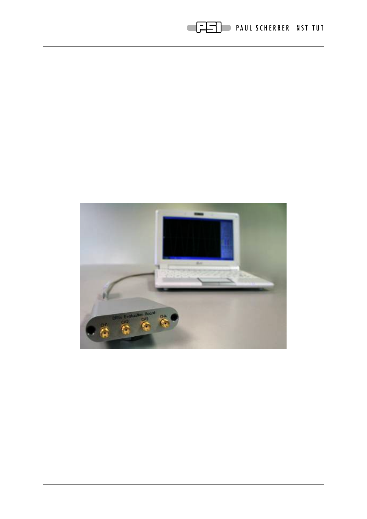
which demonstrates the basic operation of the chip. It has SMA connectors for four input
channels CH1 to CH4, an USB 2.0 connector and MMCX connectors for triggering and clock
synchronization (Figure 1). The board is powered through the USB port and contains an on-
board trigger logic. It comes with MS Windows®and Linux drivers and two application
programs. It is basically equivalent to a four channel 5 GSPS digital oscilloscope.
This manual describes the software installation, the usage of the application programs, and
gives hints for developers seeking to build new electronics around the DRS4 chip.
1.1. Board description
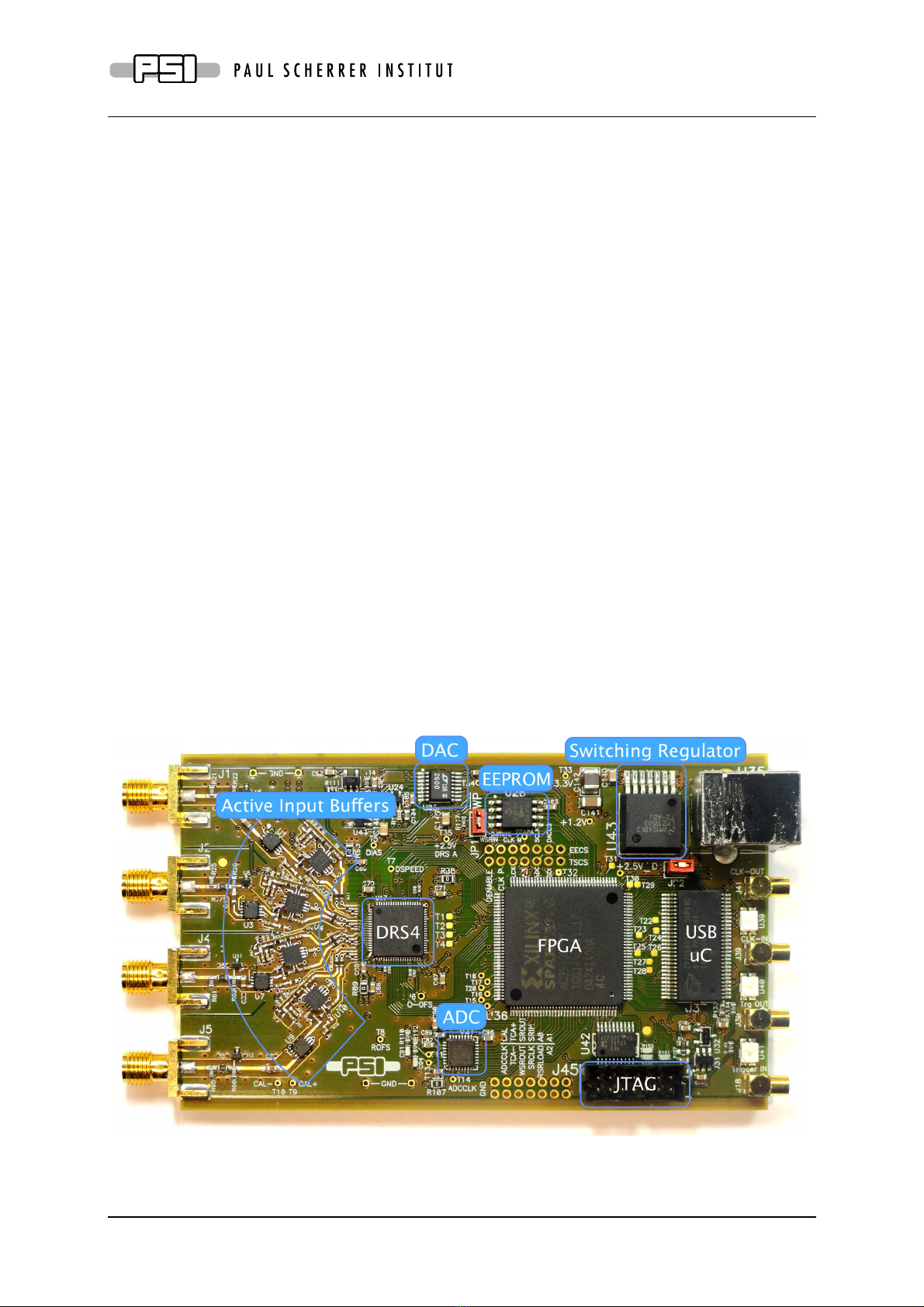
Since the DRS4 chip has differential inputs, the board uses four active buffers (THS4508
from Texas Instruments ®) to convert the 50-Ohm terminated single ended inputs into
differential signals. Analog switches in front of the buffers (ADG901 form Analog Devices®)
are used to de-couple the inputs during calibration. Two reference voltages are generated by
the on-board 16-bit DAC to measure the offset and gain of all DRS4 storage cells for
calibration. The four analog inputs are AC coupled and have a input range of 1 V peak-to-
peak. The absolute maximum input voltage range is -0.5V to +2.8V. The DRS4 is read out
with a 14-bit ADC (AD9245 from Analog Devices®) and a FPGA (Xilinx®Spartan 3). The
USB connection is implemented with a micro controller (Cypress®CY2C68013A). The high
speed modus of the USB 2.0 bus allows for data transfer rates of more than 20 MB/sec.
Figure 1: Picture of the DRS4 Evaluation Board V4 with different components
DRS4 Evaluation Board User’s Manual
Page 5 of 36
For trigger purposes and inter-board synchronization, four MMCX connectors are available,
which can be seen on the right side of Figure 1. The Trigger IN works as an external trigger
much like the one of an oscilloscope. The electrical standard is 5V TTL. Although a 50 Ω
termination is possible, the resistor is not soldered by default. This allows using weaker
sources, which cannot drive 5V into a 50 Ωload. Reflections on this line usually do not
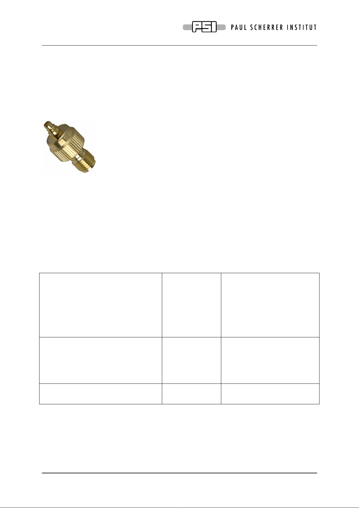
matter, since the first leading edge of the trigger is used. To connect a SMA cable to the
trigger input, a commercial adapter can be used like the one shown in.
Figure 2: MMCX-SMA adapter which can be obtained for example form
www.digikey.com (part number ACX1352-ND)
The Trigger OUT and the Clock IN/OUT signals will be supported in a future firmware
version and will allow for inter-board triggering, so that small synchronized DAQ systems
with several evaluation boards can be made.
Four on-board discriminators with programmable level allows for self triggering on any of the
four input channels, or a combination of channels supporting coincidences for example. A 1
MBit EEPROM (25LC1025 from Microchip®) is used to store the board serial number and
calibration information. Two 14-pin headers carry all important logical signals which allow
easy debugging with a logic analyzer or oscilloscope. A JTAG adapter can be used to update
the FPGA firmware through a Xilinx®Platform Cable Adapter.
The specifications of the board inputs is summarized in following table:
Analog inputs
Termination
Input range
Maximum allowed input voltage
DC
Long pulse (<2µs)
Short pulse (<200ns)
50 Ω
1 V p-p
±10V
±20V
±30V
AC coupled
Trigger input/Clock input
Termination
Maximum allowed input voltage
High Level Input Voltage
high impedance,
optionally 50 Ω
-0.5 V to +5.5 V
2.5 V (min)
5 V TTL compatible
Trigger output/Clock output
Level
5V TTL
DRS4 Evaluation Board User’s Manual
Page 6 of 36
1.2. LEDs
The DRS4 evaluation board is equipped with four LEDs. They are operated by the micro
controller and the FPGA and have following meaning:
LED
Meaning
Green
This LED becomes green when the on-board micro-controller booted
successfully. If this LED stays dark, there is either no power or the micro-
controller lost it’s program, which requires a re-programming of the EEPROM.
Yellow
When the on-board FPGA boots correctly this LED becomes lit. If it stays dark,
it might be that the FPGA program was lost and requires re-programming. After
booting, this LED indicates the board status. If lit, the DRS4 chip is active and
sampling data. If stopped by software or a trigger, this LED turns off. A special
pulse stretcher ensures that even in high trigger rate environments this LED
does not flash with more than ~10Hz so the blinking can still be seen by eye.
Red
When lit, this LED indicates a error condition
DRS4 Evaluation Board User’s Manual
Page 7 of 36
1.3. Firmware Description
Both the Windows and the Linux distribution contain a subdirectory “firmware” which
contains the FPGA and Microcontroller firmware for the DRS4 Evaluation Board. The FPGA
firmware is written in pure VHDL, thus making it easy to port it to other FPGA devices such
as Altera®or Lattice®. Only a few Xilinx®basic components such as clock managers and I/O
blocks have been instantiated and must be adapted when another FPGA manufacturer than
Xilinx®is chosen. The FPGA source code is contained in several files with following
contents:
src/drs4_eval1.vhd
Top level entity. Routing of clock signals, global reset signal,
LEDs and LEMO input
src/drs4_eval1_app.vhd
Main file containing state machines for DRS4 readout, serial
interface to DAC, EEPROM and temperature sensor, trigger
logic and reference clock generation
src/usb_dpram.vhd
Instantiates block ram for waveform storage
src/usb_racc.vhd
Interface to CY2C68013A microcontroller in slave FIFO mode.
Implements a set of status and control registers through which
the main application can be controlled
src/usr_clocks.vhd
Generates 66 MHz, 132 MHz, 264 MHz and a phase shifted 66
MHz clock out of the 33 MHz quartz input frequency via the
Xilinx®Digital Clock Managers (DCM)
ucf/drs4_eval1.ucf
Constraint file. Assigns package pins and defines clock
constraints
3s400/drs4_eval1.ise
Xilinx®ISE 9.2i project file
3s400/drs4_eval1.bit
Compiled firmware image directly for Spartan 3s400 FPGA
3s400/drs4_eval1.mcs
Compiled firmware image for FPGA EEPROM XCF02S
3s400/drs4_eval1.ipf
Xilinx®Impact project file to program FPGA via download
cable
The firmware for the USB microcontroller from Cypress®is written in C and must be
compiled with the Keil®8051 C compiler. It contains the standard include and library files
from the Cypress EZ-USB®development kit plus some DRS specific files:
CY7C68013A/drs_eval.c
Main micro controller firmware file
CY7C68013A/dscr.a51
USB descriptor tables
CY7C68013A/drs_eval.hex
Compiled firmware file (Intel HEX format)
CY7C68013A/drs_eval1.iic
Compiled firmware file (For Cypress EZ-USB Console
download)
CY7C68014A/*
Remaining files are standard files from EZ-USB development
kit

DRS4 Evaluation Board User’s Manual
Page 8 of 36
The FPGA firmware implements a set of control and status registers, through which the DRS4
can be controlled and read out. The mapping of the control registers is as follows:
#
Ofs.
Bit
Name
Comment
0
0x00
0
start_trig
Write a "1" to start the domino wave
0
0x00
1
reinit_trig
Write a "1" to stop & reset the DRS chip
0
0x00
2
soft_trig
Write a "1" to stop the DRS chip & read the data to RAM
0
0x00
3
eeprom_write_trig
Write contents of RAM into EEPROM (32kB page)
0
0x00
4
eeprom_read_trig
Read contents of EEPROM into RAM (32kB page)
0
0x02
18
led
1=on, 0=blinks once at beginning of DRS chip readout
0
0x02
19
tcal_en
Switch on (1) / off (0) 264 MHz calib. sig. for DRS chips
0
0x02
20
tcal_source
System clock (0) or separate quartz (1) clock source
0
0x02
21
transp_mode
1=send DRS inputs to outputs ("transparent mode")
0
0x02
22
enable_trigger1
Write a "1" to enable external trigger (LEMO)
0
0x02
23
readout_mode
0:start from first bin, 1:start from domino stop
0
0x02
24
neg_trigger
1=trigger on high to low transition
0
0x02
25
acalib
Write "1" to enable amplitude calibration
0
0x02
27
dactive
0:stop domino wave during readout, 1:keep it running
0
0x02
28
standby
1: put chip in standby mode
1
0x04
31..16
DAC0
Set DAC 0 (=A, ROFS)
1
0x06
15..0
DAC1
Set DAC 1 (=B, CMOFS)
2
0x08
31..16
DAC2
Set DAC 2 (=C, CAL-)
2
0x0A
15..0
DAC3
Set DAC 3 (=D, CAL+)
3
0x0C
31..16
DAC4
Set DAC 4 (=E, BIAS)
3
0x0E
15..0
DAC5
Set DAC 5 (=F, TLEVEL)
4
0x10
31..16
DAC6
Set DAC 6 (=G, O-OFS)
4
0x12
15..0
DAC7
Set DAC 7 (=H, -)
5
0x14
31..24
configuration
Bit0: DMODE, Bit1: PLLEN, Bit2: WSRLOOP
5
0x14
23..16
channel_config
1=1x8k,0x11=2x4k,0x33=4x2k,0xFF=8x1k
5
0x16
7..4
first_chn
First channel address to read out (0..9)
5
0x16
3..0
last_chn
Last channel address to read out (1..9)
6
0x18
31..16
trigger_delay
Trigger delay in ticks of roughly 2.3 ns
6
0x1A
15..0
sampling_freq
Sampling frequency in ticks (=1024/fsamp*0.120-2)
7
0x1E
31..16
trigger_config
Trigger configuration
7
0x1E
15..0
eeprom_page
Page number for EEPROM communication
While the mapping of the status registers is like this:
#
Ofs.
Bits
Name
Comment
0
0x00
31..16
board_magic
0xC0DE, Magic number for DRS board identification
0
0x02
15..8
board_type
5: Eval. Board V2; 7: Eval. Board V3
0
0x02
7..0
drs_type
4 for DRS4
1
0x04
0
running
"1" while domino wave running or readout in progress
2
0x08
31..16
stop_cell
position of cell where sampling stopped at last trigger
8
0x20
31..16
temperature
temperature in 0.0625 deg. C units
9
0x24
31..16
serial_cmc
Serial number CMC board
9
0x26
15..0
version_fw
firmware version (SVN revision)
All registers are implemented as 32-bit registers, so they can be mapped easily into some
VME address space for example if one decides to build a VME board containing the DRS4.

DRS4 Evaluation Board User’s Manual
Page 9 of 36
2. Installation
2.1. Windows XP
Under MS Windows®it is important to install the necessary driver before connection the
DRS4 Evaluation Board with the PC. The current distribution can be downloaded from
http://drs.web.psi.ch/download . The Windows version contains a single program drs-
xx.exe (where xx is the version) which can be executed to install the driver, applications,
documentation and source code. Executing this file starts the installer:
You can select which components to be installed:

DRS4 Evaluation Board User’s Manual
Page 10 of 36
Then you can select the installation directory:
After the installer has finished, you can connect the DRS4 Evaluation Board to the Computer:
Now you will see the “Found New Hardware” dialog:
Where you can click “Install the software automatically” and then click “Next”.

DRS4 Evaluation Board User’s Manual
Page 11 of 36
After successful installation of the driver, you will see the following window:
And a new group in your Start Menu:
The software comes with two applications, a command line interface and an oscilloscope.
These applications are explained in section 3.
DRS4 Evaluation Board User’s Manual
Page 12 of 36
2.2. Windows 7
The installation under Windows 7 (32 and 64 bit) is basically the same than for Windows XP.
You need the DRS software version 3.0.1 or later if you are using a 64-bit system, since
version 3.0.0 and prior does not contain the 64-bit version of the libusb library. When you
start the software installation, you get an additional screen which you have to confirm:
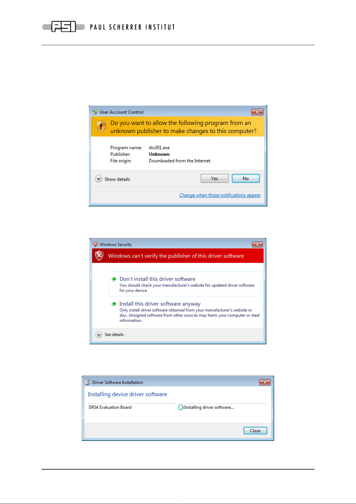
Make sure that you are logged in as an administrator to install the software. During the
installation process, you will see a notice about some unverified driver software. Please select
“Install this driver software anyway” to install the driver.
After the software has been installed, you can connect the DRS4 Evaluation Board to the
computer. The driver installation should then start automatically and you will see this
notification:
When this has finished, you can start the “drscl” and “drsosc” programs.

DRS4 Evaluation Board User’s Manual
Page 13 of 36
2.3. Linux
The drivers and applications are distributed for Linux in source code and must be compiled on
each system. First untar the tar ball:
[/usr/local]$ tar -xzvf drs-1.0.tar.gz
drs-1.0/
drs-1.0/doc/
drs-1.0/doc/DRS4_rev06.pdf
drs-1.0/doc/manual.pdf
drs-1.0/include/
drs-1.0/include/ConfigDialog.h
drs-1.0/include/DOFrame.h
drs-1.0/include/DOScreen.h
. . .
Then change the directory and do a „make“. Note that to compile the oscilloscope application
it is necessary to have the wxWidgets package version 2.8.9 or later installed. You can obtain
this package in source form from http://www.wxwidgets.org/downloads/. If this package is
present, you can change to the drs directory and issue a make:
[/usr/local]$ cd drs-1.0
[/usr/local/drs-1.0]$ make
g++ -g -O2 -Wall -Wuninitialized -fno-strict-aliasing -Iinclude -DOS_LINUX
-DHAVE_LIBUSB -c src/musbstd.c
g++ -g -O2 -Wall -Wuninitialized -fno-strict-aliasing -Iinclude -DOS_LINUX
-DHAVE_LIBUSB -c src/mxml.c
. . .
Now you can connect the DRS4 board to the PC. On systems where the “lsusb” tool is
installed, one should be able to find the DRS4 evaluation board after connecting it with
following command:
[/usr/local/drs-1.0]$ /sbin/lsusb -d 04b4:1175 –v
Bus 005 Device 005: ID 04b4:1175 Cypress Semiconductor Corp.
Device Descriptor:
bLength 18
bDescriptorType 1
bcdUSB 2.00
bDeviceClass 0 (Defined at Interface level)
bDeviceSubClass 0
bDeviceProtocol 1
bMaxPacketSize0 64
idVendor 0x04b4 Cypress Semiconductor Corp.
idProduct 0x1175
bcdDevice 0.01
iManufacturer 1 S. Ritt PSI
iProduct 2 DRS4 Evaluation Board
iSerial 3 REV1
bNumConfigurations 1
Configuration Descriptor:
bLength 9
bDescriptorType 2
wTotalLength 46
bNumInterfaces 1
bConfigurationValue 1
iConfiguration 0
bmAttributes 0x80
MaxPower 500mA
. . .

DRS4 Evaluation Board User’s Manual
Page 14 of 36
If the board is correctly recognized, one can access it with the command line program. Under
most Linux distributions however, only the “root” user can directly access USB devices.
Some systems can be configured to allow non-root access via the “udev” system, but the exact
instructions vary from distribution to distribution and can therefore not be given here.
If the command line program works, the oscilloscope application “drsosc” can be started. It
will open a X window and show exactly the same functionality as its Windows counterpart:

DRS4 Evaluation Board User’s Manual
Page 15 of 36
3. Running the Board
3.1. Command line Interface “drscl”
Clicking on „DRS Command Line Interface“ (Windows) or entering “drscl” (Linux) will start
a simple application which connects to the DRS4 Evaluation Board. If it finds the board, it
displays the board serial number and the firmware revision as on the following screen shot:
Now you are ready to issue your first command “info” which shows some more information,
like the current board temperature. The temperature sensor is on the bottom side just below
the DRS4 chip. If you keep issuing “info” commands and touch that sensor with your finger,
you should see the temperature increase.
3.2. Oscilloscope application “drsosc”
The second application is an oscilloscope-like program, which connects to the DRS4 board
and works pretty much like a normal oscilloscope. You can select the trigger mode, trigger
level and trigger source. On Rev. 1.1 of the DRS4 evaluation board, only CH1 can be selected
as trigger source. You enable a channel by clicking on the number “1” to “4”. There are two
cursors and a few utilities.

DRS4 Evaluation Board User’s Manual
Page 16 of 36
The picture above shows an un-calibrated evaluation board, which shows a noise level of
about 8 mV RMS. After offset and gain calibrations, the noise level is reduced significantly:
The evaluation board Rev. 3 still shows some small random spikes. It is expected that future
versions will improve this and reduce the noise level further.

DRS4 Evaluation Board User’s Manual
Page 17 of 36
The DRS4 evaluation board is shipped pre-calibrated in amplitude and time. This calibration
can be turned on or off using the check boxes “Display calibrated waveforms” and “Display
timing calibrated waveforms” in the “Config” Dialog:
The calibration can be re-done any time by clicking on the “Execute Voltage Calibration” and
“Execute Timing Calibration” buttons. For the voltage calibration, the inputs are switched to a
calibration voltage generated by a DAC. Three calibration points (-0.4V, 0V, +0.4V) are
taken and an offset and gain is evaluation. For the timing calibration, an internal 240 MHz
clock is sampled in one channel and the deviation from the expected period to the measured
period is used to determine the effective width of each cell. Following picture shows the result
of such a timing calibration done at 2 GSPS. The effective bin width deviates only slightly
from the nominal value of 0.5 ns, but the integral timing nonlinearity adds up to almost 1 ns,
which is typical for the DRS4 chip. Since transistor parameters have normally gradients over
the chip wafer, SCA chips are usually “faster” on one side compared to the other.

DRS4 Evaluation Board User’s Manual
Page 18 of 36
This calibration data both for voltage and timing is then stored in the EEPROM on the
evaluation board, from where it is obtained each time the oscilloscope gets started. This
assures that a board is calibrated even when used on different computers. Note however that
the timing calibration is only valid for some sampling speed. So if you want to run the board
at a different speed, you have to redo the timing calibration at that speed. The voltage
calibration is a bit less dependent on the sampling speed, there is however some dependence
on temperature. It is advised to keep the board running for a few minutes until the temperature
shown in the status bar stabilizes before doing a voltage calibration.

DRS4 Evaluation Board User’s Manual
Page 19 of 36
For test purposes, an internal 60 MHz reference clock signal can be connected to channel #4
via the “Config” menu. To do so, activate channel #4, then select the “Config” menu and
click on “Connect reference clock to channel #4”:
The effect of the timing calibration can be tested by turning the timing calibration on and off
via the “Display timing calibrated waveforms” check box.

DRS4 Evaluation Board User’s Manual
Page 20 of 36
You can save a waveform in an ASCII and a binary format by pressing the “Save” button.
After you open a file, each trigger will write the waveform of the active channel(s) to that file.
When you are continuously running, the file will grow very quickly. If the file has the
extension “.xml” it will be written in ASCII form using XML encoding, otherwise a raw
binary file will be written. Here is a snipped of such an XML file:
<?xml version="1.0" encoding="ISO-8859-1"?>
<!-- created by MXML on Tue Feb 15 13:05:04 2011 -->
<DRSOSC>
<Event>
<Serial>1</Serial>
<Time>2011/02/15 13:05:04.758</Time>
<HUnit>ns</HUnit>
<VUnit>mV</VUnit>
<CHN1>
<Data>20.7,-63.7</Data>
<Data>21.7,-62.3</Data>
...
<Data>1033.4,424.9</Data>
<Data>1034.4,423.3</Data>
</CHN1>
<CHN2>
<Data>20.7,-8.5</Data>
<Data>21.7,-7.0</Data>
...
<Data>1033.4,-8.3</Data>
<Data>1034.4,-8.2</Data>
</CHN2>
</Event>
<Event>
<Serial>2</Serial>
<Time>2011/02/15 13:05:04.883</Time>
<HUnit>ns</HUnit>
<VUnit>mV</VUnit>
<CHN1>
<Data>20.6,-63.0</Data>
<Data>21.6,-63.8</Data>
...
Each individual event contains a header with the serial number of that event (starting with 1),
and the date/time it was recorded. Then there is the channel data with pairs of time (in ns) and
voltage (in mV). The number of channels depend on which channel was on when the data was
recorded. It might be a single channel (CHN1) or all four channels (CHN1-CHN4). Please
note that the XML format requires more space on your storage and takes also more CPU
power to be written, so the maximum data rate is limited.
Other manuals for DRS4
2
Table of contents
Other PSI Motherboard manuals


