Siera SG 1420N User manual

CHASSIS CTS-AA
SERVICE MANUAL
SERVICE MANUAL

2
CONTENTS Page
1.-Technicalspecifications 3
2.-ConnectionFacilities 3
3.-Mechanicalinstructions 4
4.-Oscillograms 5
5.-Printboardlayout 6
6.-ElectricScheme 7 - 11
7.- Circuit description 12
7.1 Small signal processing 12
7.2 RGB ampliers 14
7.3 Deflection 14
7.4 Sound amplifier 15
7.5 Powersupply 15
7.6 Microcontroller/Text 17
8.-Electricaladjustments 18
9.-Safetyinstructions 21
10.- List of abbreviations 22
11.-Servicecomponents 23

3
1. Technical specifications
CHASSIS CTS - AA
Mains voltage : 220 - 240 V ± 10% AC; 50 Hz (±5%)
Power cons. at 220V~ : 35W (14''), 50W(20''/21''), 5W (stand by)
Aerial input impedance : 75S- coax
Min. aerial input VHF : 30µV
Min. aerial input UHF : 40µV
Max. aerial input VHF/UHF : 180mV
Pull-in range colour sync. : ± 300Hz
Pull-in range horizontal sync. : - 600 Hz / + 480 Hz
Pull-in range vertical sync. : ± 5 Hz
Picture tube range : 14'' / 20'' /21''
: Mono: 25S 1W (14''). 16S2W (20''/21'')
TV Systems : PAL BG
: PAL I
:PAL BG / SECAM BGDK
:PAL BGI / SECAM BGLL'
Indications : On screen display (OSD) / menu
: 1 LED RED. Dark in ON, bright in stand by,
blinking with RC.
VCR programs : 0 to 99
Tuning and operating system : VST
UV1315A / IEC (VST) : VHFa: 48 - 168 MHz
: VHFb: 175 - 447 MHz
: UHF: 455 - 855 MHz
U1343A / IEC (VST) : UHF: 471 - 855 MHz
Local operating functions :Vol/Prog, +, -, contrast, colour and brightness.
2. Connection facilities
Euroconector:
1 - Audio R (0V5 RMS / 1K ). 17 - CVBS
2 - Audio R (0V2 - 2V RMS / 10K ). 18 - CVBS
3 - Audio L ( 0V5 RMS / 1K ). 19 - CVBS ( 1Vpp 75S).
4 - Audio 20 - CVBS ( 1Vpp/75S).
5 - Blue 21 - Earthscreen.
6 - Audio L (0V2 - 2V RMS / 10K ).
7 - Blue (0V7pp/75S).
8 - CVBS status 1 (0-2V int., 10-12V ext.).
9 - Green
10 - -
11 - Green (0V7pp/75S).
12 - -
13 - Red Head phone:
14 - -
15 - Red (0V7pp/75S). 8Sto 600S(32S25mW)
16 - RGB status (0V to 0V4 int.) (1-3V ext. 75S).

4
Fig.3.1
For the main carrier two service positions are possible (3.1).
A: For faultfinding on the component side of the main carrier.
B: For (de) soldering activities on the copper side of the main carrier.
Position A can be reached by first removing the mains cord from it's fixation, then loosen the carrier lips (1) and then pulling the
carrier panel (2) for approximately 10cm.
Position B can be reached from position A after disconnecting the degaussing cable.Put the carrier on the line transformer side.
3. Mechanical instructions
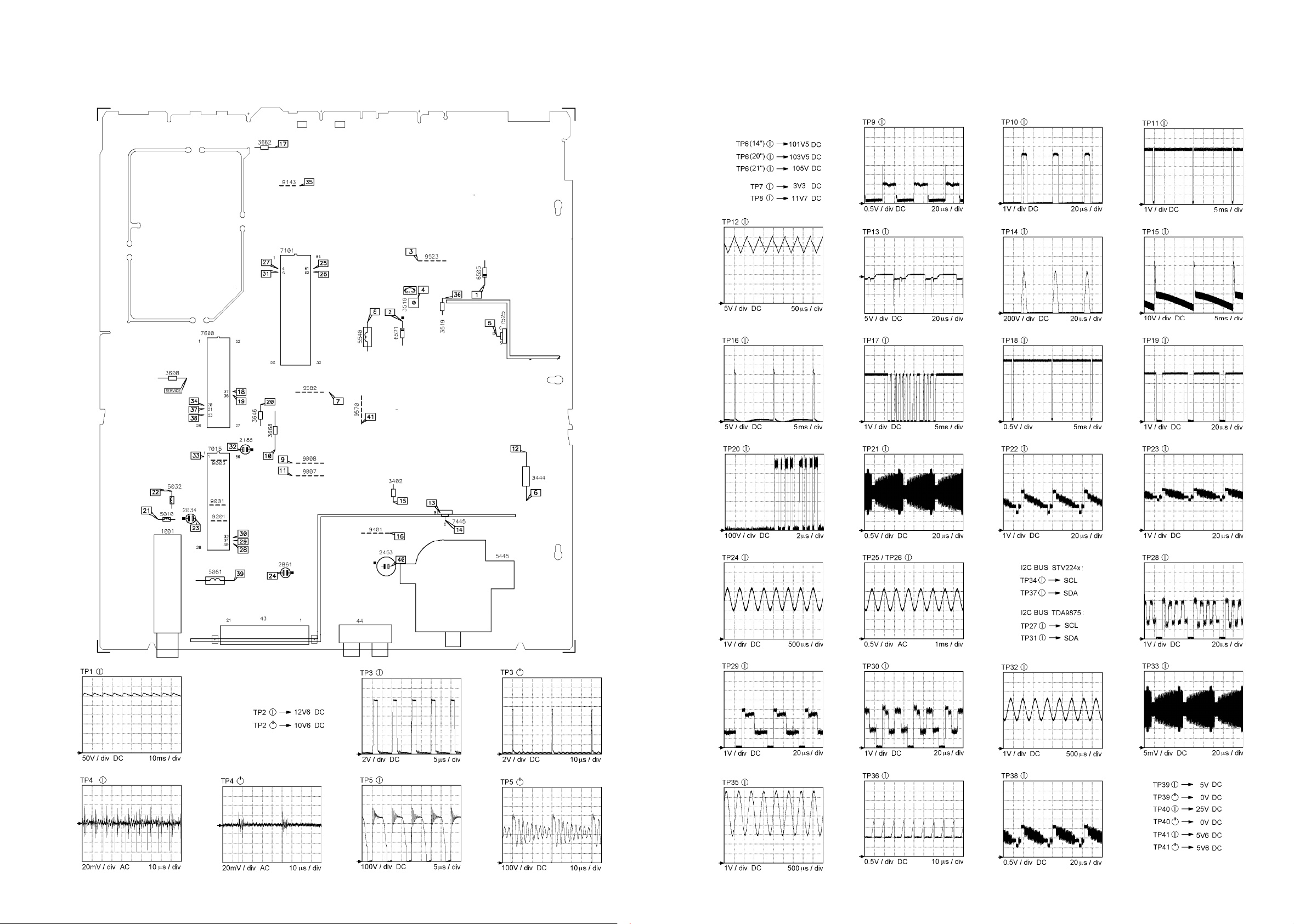
4. Oscillograms
5

5.- PRINT BOARD LAYOUT
6

3281 F3
3284 K2
3285 K2
3286 L2
3287 K2
3288 K3
3289 K3
3291 K3
3294 L3
3330 E2
3331 F2
3335 H2
3346 E3
3351 D3
3371 E3
3372 D2
3373 E2
3715 F8
5010 D8
5012 D8
5032 F8
5040 H7
5060 F7
5067 C2
6014 C8
6020 E8
6115 B8
7015 G5
7127 C8
7274 K3
7275 L3
7276 L3
7372 D2
9001 A2
9002 G3
9003 M6
9004 E7
9006 G2
9007 E3
9008 E2
9009 D2
9010 A2
9012 M9
9013 M9
9014 M8
9016 A3
9018 B2
9019 B2
9020 M6
9021 M6
9022 M7
9023 M8
9174 M5
9200 B2
9201 M7
9561 A2
9656 E3
6.- Electric Diagram 1015 D6
1032 G8
1033 F8
1137 B7
1272 H3
2010 D7
2011 D7
2013 D8
2014 D8
2015 H6
2016 H6
2017 E9
2018 E7
2024 C6
2025 D6
2026 C6
2027 C6
2028 E6
2029 E6
2034 I7
2060 F7
2061 F6
2064 F3
2065 F3
2067 C3
2068 C3
2115 B6
2117 B9
2180 B3
2185 B3
2240 K7
2242 J2
2243 J2
2244 J2
2245 M2
2250 J6
2261 H3
2262 H2
2270 I3
2289 F3
2291 L7
2292 L7
2293 K7
2294 J7
2350 D3
2351 D3
2801 I7
2861 F8
3010 D7
3011 C7
3012 D7
3017 E8
3018 E8
3019 E8
3020 E8
3021 E8
3028 E7
3032 G7
3033 I7
3034 I7
3035 G8
3069 D2
3070 D2
3115 B6
3117 B8
3118 B8
3119 B8
3120 C8
3121 C8
3185 C3
3240 K6
3262 H3
3274 K3
3275 K2
3276 L3
7

2204 C6
2208 E3
2209 D3
2217 D6
2230 F6
2402 G7
2403 H6
2404 I8
2405 I7
2406 I5
2407 H5
2408 K7
2410 H4
2411 I4
2430 H3
2440 M6
2442 M6
2444 L6
2445 L5
2446 L4
2448 K5
2449 K5
2450 L7
2451 L6
2453 M2
2458 J4
2460 K3
2462 L3
2470 K5
3201 A5
3202 A6
3203 B4
3204 B6
3208 B6
3210 B7
3211 D7
3212 E7
3214 C5
3215 C6
3216 C5
3217 D6
3221 D6
3225 E6
3226 E3
3228 D3
3229 E5
3230 E6
3233 D5
3234 D6
3235 L4
3238 M4
3243 E5
3244 E6
3400 G8
3401 I8
3402 H7
3403 H7
3404 I7
3405 I7
3406 H6
3407 H5
3408 I6
3409 I6
3410 H6
3411 I7
3412 I7
3413 I5
3414 I5
3416 I4
3417 I4
3418 H5
3430 G4
3431 H4
3432 G4
3433 G3
3434 H3
3440 M7
3442 M6
3444 L7
3445 L5
3449 M3
3451 L6
3455 K7
3456 K6
3457 J5
3460 K3
3461 K4
3462 K3
3463 H2
3470 K4
3480 L6
5201 D4
5202 D4
5440 M7
5441 L6
5445 L4
5447 J4
5449 M3
5480 L6
6201 A5
6218 C5
6225 F6
6227 D5
6243 F5
6401 H5
6447 L4
6449 M3
6451 L6
6462 H2
6470 K5
7201 A5
7204 B5
7205 B6
7208 C5
7209 C5
7210 C6
7211 D5
7212 E5
7213 E6
7401 G6
7430 G4
7431 G3
7440 M6
7445 L5
9204 B5
9212 E5
9214 D7
9217 E7
9220 E7
9221 C7
9401 G5
9402 H7
9404 I6
9417 I5
9480 K6
6.- Electric Diagram
8

1001 B7
2001 B8
2002 B6
2005 D7
2006 C7
2090 C8
2091 D8
2092 D8
2179 K3
2182 K3
2184 K4
2186 L6
2187 G7
2188 G7
2189 K6
2190 G7
2191 K6
2192 H7
2194 H6
2195 K6
2197 L6
2800 F2
2850 F3
2852 E3
2856 E2
2857 F4
2859 F2
2860 F4
2876 B4
3000 D8
3002 C9
3003 C8
3004 C9
3005 C8
3006 D9
3007 D8
3008 D8
3026 D8
3186 K5
3187 L6
3190 G8
3191 H7
3193 I6
3194 I5
3197 I6
3808 F3
3809 E4
3810 E2
3841 E5
3843 D5
3845 C5
3850 F2
3851 E3
3852 E2
3853 D3
3854 E2
3855 C3
3856 F2
3858 C3
3860 E4
3865 B2
3875 B4
3876 C4
3877 B4
3879 D2
3880 E2
3881 D1
3883 E1
3891 C2
3893 G3
5061 B7
6848 C2
6849 B2
6851 E4
6852 E4
6853 D4
6854 D4
6855 D4
6856 D4
6857 D5
7187 J4
7187 K6
7875 B5
7876 D2
9102 L6
9143 J3
9169 H7
9170 H5
9181 H5
9182 L4
9190 G8
9801 B4
9802 F2
6.- Electric Diagram
9

10
1500 C1
1540 I4
1541 H2
2500 D2
2502 F2
2503 E2
2504 F2
2505 F2
2506 H5
2507 E2
2508 F4
2509 D4
2510 D4
2511 E4
2514 F3
2515 F4
2516 G2
2522 G3
2523 E3
2524 G3
2530 I2
2532 H4
2534 H2
2540 I4
2561 K2
2562 J2
2563 K4
2564 I3
2565 I3
3500 G2
3501 E2
3502 J4
3503 L4
3504 B2
3505 K5
3507 F2
3508 E4
3509 C4
3510 D4
3512 F4
3516 G2
3517 F4
3518 E4
3519 D3
3520 D2
3521 G3
3522 G3
3523 F3
3524 C2
3525 C3
3527 G4
3528 G4
3570 J3
3571 K3
3573 K3
3574 I3
3575 J5
3576 J3
3577 I3
5500 D2
5525 H3
5531 J2
5532 H4
5534 H2
5540 K4
5552 G2
6502 F2
6503 F2
6504 F2
6505 F2
6515 F4
6516 G2
6521 F3
6530 I2
6540 H4
6541 H2
6570 J3
6571 J3
6572 J4
6573 I3
6574 K4
7501 J5
7502 J4
7514 E3
7525 G3
7571 J3
7575 J2
7577 I2
9501 K2
9503 B1
9506 E5
9523 E3
9524 D4
9541 I5
9570 J3
9582 K5
9598 C2
9599 C1
6.- Electric Diagram

1679 G3
1685 F2
2149 E2
2600 D3
2602 C7
2610 D7
2611 D8
2636 K7
2641 K3
2648 L7
2651 B3
2660 F2
2669 I2
2677 H3
2680 G3
2681 G3
2682 F3
2685 F2
2691 F3
2692 F8
3149 E3
3601 B8
3602 B8
3603 C7
3604 C7
3605 C7
3606 C6
3607 C6
3608 E7
3609 F7
3610 C7
3611 C8
3612 C8
3616 D2
3617 E2
3618 F7
3619 G7
3620 F6
3621 D7
3636 L7
3637 K7
3643 K3
3644 J3
3645 J3
3646 J3
3647 K3
3648 L7
3649 J3
3650 J4
3651 J4
3652 I3
3653 K4
3656 E3
3657 E3
3658 E3
3659 E3
3660 F2
3661 I7
3662 F3
3663 J7
3664 J8
3665 G8
3666 J7
3667 G8
3668 I2
3669 I2
3670 I3
3673 I8
3674 J8
3675 K8
3676 F3
3681 I7
3684 D3
3685 D3
3687 K3
3691 B2
3692 B2
3696 J8
6149 E3
6602 C7
6663 J7
6691 C2
7600 H5
7605 C7
7657 E2
7659 E2
7670 I3
7673 I8
7685 D3
7691 B2
9504 B8
9607 L2
9652 I3
9674 L8
9675 L8
9678 L2
9679 M2
9685 L2
9696 B8
6.- Electric Diagram
11

STV2248:
STV2246:
Figure 7.1 TV Processor block diagram

12
7.- CIRCUIT DESCRIPTION
7.1 SMALL SIGNAL PROCESSING (Diagram A)
Thesmall signalis processedby IC 7015(STV2246 for Palsets, STV2248for Pal/Secamsets), includingIF detection,
videoprocessing, chroma decoder,RGB ,syncprocessor andsound decoder.TheICsSTV2246 andSTV2248 arefully
controlled by I2C bus and their block diagram can see in fig. 7.1.
7.1.1 IF detection
IF detection can be intercarrier (no multistandard sets), that means sound and picture are detected in the same circuit
(PIF), or QSS (Quasi Split Sound, used in multistandard sets) where sound is detected in a separated circuit (SIF).
-PIFinput (pins6, 7):TheIF signalcoming from pin11ofthe tuner(diagramC) isfiltered bytheIF SAW filter (1015)and
applied to PIF input of IC7015 (pins 6 and 7). The IF bandpass characteristic is determined by the SAW (Surface
AcousticWave)filter.
-PIF oscillator(pins 9,15, 16): ThePIF PLL(phase locked loop) is based on a LC resonator (L5040). Carrier frequency
should be adjusted by I2C bus at 38.9 MHz (see chap. 8.3). A filter for the PLL is present at pin 9 (2028, 2029, 3028).
AFC is internally controlled for the µC (7600 diagram E) by I2C. Identification signal is also internal.
- AGC (pins 5, 8): The IF AGC time constant is fixed by the capacitor 2025 (pin 5). The AGC delayed voltage (pin 8) is
applied to pin 1 of the tuner and adjusted by I2C (see chap. 8.4).
-Videooutput (pin13): Thisbaseband CVBS signal with2Vpp ofnominalamplitude, containstheFM intercarriersound
signal.Sound is filteredout bya ceramic trap(1032 or1033) whichfrequency can bedifferent dependingon the system:
5.5 MHz for BG, 6.0 MHz for I or 6,5 MHz for DK.
Multistandardsets
- The IC STV2248 is used in multistandard sets.
-Only picture IFis processed inPIF circuit (pins6,7), and carrier frequency has a second adjustment (by I2C) at
33.9MHz for L’ standard (see chap. 8.3). The IC changes automatically between negative (BGIDK) and positive
(LL’)modulation.
- Sound IF is processed in SIF circuit (QSS system)
- SIF input (pins 1, 2): Sound is filtered from IF signal in a SAW filter K9650 (1137). The IF input is present at pin
1 of 1137 and pin 2 is used as a switching input:
- If Vpin2 = 0V a 40.40MHz sound carrier is filtered (for L´ system, L/L´ signal is high, T7127 conducts).
- If Vpin2 = Vpin1 a 33.40MHz sound carrier is filtered (for L,I,BG systems, L/L´ signal is low, T7127 is cut,
D6115conducts).
- SIF AGC (pin 3): The sound IF AGC time constant is fixed by the capacitor C2024.
7.1.2Sound processor
- FM demodulation: For intercarrier sets (no multistandard) FM sound is filtered internally from CVBS (pin 13) and
demodulated. De-emphasis is also made internally. If the set is Pal/Secam BG or DK, STV2248 is used instead of
STV2246.SIF inputand AMdemodulator are avoided and pins1, 2are ACgrounded by C2115.
- Scart audio out (pin 11): The signal at this pin is drived to the euroconnector sound outputs (see Diagram C).
- External audio in (pin 14): External audio proceeding of pins 2,6 of euroconnector is applied to this pin. Selection
betweeninternal orexternal is done by aninternal switching controlled by I2C(see INT/EXT, chapter7.6).
-Audioout(pin55): After avolumecontrol(by I2C), thisoutputisdrivedto the inputIN+ofthefinal soundamplifierIC7187
(DiagramC).
Multistandardsets:
FM demodulation: This function is done in the same internal circuit of STV2248 that no multi sets, but the input
proceeds of SIF circuit, instead of CVBS signal.
AM demodulation: In Multistandard sets, also AM demodulation for LL’ systems is necessary. AM sound is
extracted directly from the SIF inputs by an internal circuit.
AM/FM switch : This internal switch is commanded by the µC depending on the system selected on the tuning
menu.
7.1.3 Video processing
- Video switches (pins 18, 20, 44): The internal CVBS signal is now fed to pin 18 IC7015. External CVBS proceeding
frompin20of Euroconnectorispresenton pin20of7015. TheICswitchesbetween internalandexternalby I2Cbus(see
INT/EXT, chapter 7.6).At pin 44 there isan outputof CVBS usedfor theTXT decoder.

13
-Luminanceprocessor:CVBScomingfromvideo switches isinternallyappliedtoluminanceprocessor,whichiscomposed
of chrominance trap filter, luminance delay line and peaking circuits. Sharpness control modifies peaking by I2C.
- Black stretch circuit (pin 21): This feature of the picture is fixed (not adjustable). Black stretch capacitor 2250 is
connected to pin 21.
7.1.4 ChromaDecoding
-ACCand chromafilter: Video signalcoming fromvideoswitches, goesthrough an internalvariable-gain amplifiertothe
chroma band pass filter. Gain of amplifier is determined by burst amplitude (ACC). If the amplitude of chroma signal is
higherthan standard,an additionaloverload circuitdecreases it(ACCO).
-XTAL(pin 40): The VCO uses one 4,43MHz crystal connected to pin40.
PAL sets:
STV2246is used.Bandpass filterand demodulator are fully integrated.
Demodulatorconsist ofsynchronous detectors.
PLL is locked during the burst gate time window.
- CLPF (pin 41): The voltage on this chroma PLL filter controls the VCO in order to have the right frequency and
phaseaccording burstsignal.
PAL/ SECAM sets:
STV2248 is used. Pal or Secam signals are recognized automatically by the IC.
Pal decoding is the same as in STV2246.
Secam demodulation is based on a PLL with automatic calibration loop.
-Secam bellfilter (pin38): Centralfrequency ofbell filter (4.286 MHz)is finetuning duringframe blanking,using
theXTAL frequency(4.433MHz) as a reference.Tuningcontrolvoltage is stored inC2270.
- Chroma DL: The outputs of the demodulator are applied to an internal chroma delay line. Line number n is delayed
64useg and added to n+1 obtaining U and V signals (R-Y and B-Y).
7.1.5 RGB processor
-External RGBinputs (pins 25, 26, 27):RGB inputscoming fromscart (see diagram C), areAC coupled(C2291/92/93)
and converted internally in YUV signals (RGB TO YUV). Then are switched with internal YUV (YUV SWITCH) by fast
blanking.
- Fast blanking external (pin 28): When fast blanking is high external RGB is displayed, only if TV is in external AV
(program 0). Fast blanking can switch signals for full screen (by a DC voltage) or for a part of the screen (by a pulse
voltage).
-Matrix: After switching, YUV signalsare convertedto RGBin theinternal MATRIXcircuit.Saturation control is received
from the µC by I2C bus.
-APR(pin24): The APRcircuit(AutomaticRGB Peak Regulation)compensatesthespread ofcontrastbetweensources.
If one of RGB signals exceeds the APR threshold, 2440 is charged and the gain is decreased. APR threshold can be
adjustedin Service menu.
-RGB OSD(pins 36,35, 34):RGB inputsfor OSDand TXTcoming fromµC (7600diagram E),are ACcoupled (C2242/
43/44)and applied toa RGB SWITCHcontrolled for theµC by fastblanking input (pin37).
Videocontrols: Contrast, brightnessand saturation areadjusted by I2C for the µC.
- BCL input (pin 46): Beam current is limited by circuit BCL/SAF. When beam current is high, voltage of C2460 is lower
(DiagramB),D6462 conductsand Vpin46islower.When Vpin46< 5.75V firstcontrast andthen brightness arereduced.
- Safety input (pin 46): BCL/SAF circuit has also a safety function. If frame deflection is broken down, T7431 conducts
(Diagram B), Vpin46 = 0V and line deflexion (pin 48) is disabled .
- RGB output circuit (pins 32, 31, 30): RGB outputs are drived to RGB amplifier (Diagram B).
-Digital cut-offloop (pin 33):Cut-off looppermits to controlautomatically thecut-off point of the 3RGB cathodes by DC
level. At the end of the frame blanking 3 consecutive cut-off lines, B, G and R are created. Cut-off current flows across
T7204,T7209andT7212 (DiagramB)respectivelyand itismeasuredon pin 33.WhenVG2 voltage isadjusted,DC level
of RGB outputs is adapted to keep cut-of current.
-Warm-updetection circuit(pin 33):Atthe startup picture isblanked and3 white linesare drived,insteadof cut-offlines.
As soon as the start beam current is detected on pin 33, RGB circuit starts in normal operation. If RGB circuit is
damaged or grid 2 is low, the RGB circuit could not start (black picture) due to current is not detected.
7.1.6 Horizontal synchro
- Start up (pins 45, 53): The horizontal oscillator starts running when supply voltage of pin 45 reaches 6V and supply
voltageofpin 53 reaches4V.During startupcircuit provides asofteroperating horizontaloutputwith a75%of duty cycle.

14
Note: The set do not start up if protection voltages are activated (Vpin 49 > 2.5V or Vpin46 < 1V)
- Hor. sync. separator: Fully integrated sync. separator with a low pass filter, slicing level at 50% of the synchronized
pulseamplitude.
-Horizontal 1st loop circuit (pin50): Thefirst phaselocked loop(PLL1) locks the internal linefrequency referenceon the
CVBSinput signal.It iscomposed ofan internal VCO (12MHz) that requires thechroma referencefrequency (4.43MHz
atpin40),adividerby768,alinedecoderandaphasecomparator.ScanningPLL1filter(SLPF)needsexternalcomponents
onpin 50. PLL1time constantis automatically controlledby softwarefor broadcasting signals.For videosignals (AVand
program 99) constant is always fast to prevent top bending on the screen.
-LBF(pin49): Line FlyBackinput,is obtained bythenetworkR3456/55 (Diagram B),T7372andR3371. Output ofT7372
isused also as HSYNC ofthe µC (pin 36 IC7600diagram D). When the DCvoltage of pin 49 ishigher than 2.5V, HOUT
(pin48) isinhibited (protection).
- SSC output (pin 49): Super Sand Castle output is used only internally. Levels of sandcastle pulse are 5V for burst
detection,3V for line blanking and2V for frameblanking.
-Horizontal2nd loopcircuit: The flybackposition respectline blanking onTRC cathodeiscontrolled inthis circuit.Phase
can be adjusted by I2C.
-HOUT (pin48): Horizontaloutput is an open collector which onedrives thehorizontal driverstage (T7440 diagram B).
7.1.7 Vertical synchro
- Vert. sync. separator: It is an internal integrator to separate frame sync. pulses from CVBS.
-Verticaloscillator:Verticalfrequencyis obtainedinternallyfrom line frequencybya line counter.Modeusedis automatic
50/60Hzidentification with50Hz priority.
- Vert. output stage (pin 43): This pulse output is used to drive the sawtooth generator in the vertical amplifier (pin 3
IC7400diagramB) and alsoasVSYNC of theµC(pin 37IC7600diagram D). TheVERTpulse period is314lines in50Hz
freerunningmode(264 in 60Hz)and312.5 lines in50Hzsynchronizedmode (262.5in60Hz).Frame blankingisfromline
2 to 12.5.
-Vert.amplitude (pin 42): ThisDC outputis appliedby a dividerresistor (R3416,R3414 diagramB) topin 4 ofIC7400 to
controlvertical amplitude. It can be adjusted byI2C from 1.5V (max. vert. amplitude) to6V (min. vert. amplitude).
7.2 RGB AMPLIFIERS (diagram B)
- RGB inputs : The inputs of RGB amplifiers come from pins 32, 31 and 30 of IC7015 (Diagram A). White D is adjusted
inIC7015 changingthe AC levelof theinputs by I2Cbus andcut-off changing the DC level.
-RGBamplifiers (7205,7210, 7213): RGBcircuit consistof3 inverteramplifiers (7205, 7210,7213) includingactiveload
(7201, 7208, 7211). To improve high frequency amplification there are small capacitors (2204, 2217 and 2230), and to
adaptDC levelfor inputs there is adiode (6225).
-Cutoff control(7204,7209, 7212):Cathodecurrent producedatcut-off pulses,is applied tocut-off control circuit,pin 33
ofIC7015 (see5.1.5), acrosstransistors (7204,7209, 7212).Diode 6243is addedto preventhigh voltage in IC7015.
- Flash-over protections: Clamping diodes to +200V (6201, 6218, 6227) and 1K5 series resistors (3203, 3216, 3326,
3228,3229) are addedfor protectthe circuit fromTRC flash-over.
7.3 DEFLECTION (Diagram B)
7.3.1 Framedeflection
Thisfunction isperformed bythe integratedcircuit TDA1771(7401).
- Frame supply (pins 2, 9, 10): Pin 9 is used to supply the IC except output stage which one is supplied by pin 2. At pin
2 there is a higher voltage during flyback time. This is produced adding the flyback signal present at pin 10 to a +25V
supplyby D6401and C2410.
-Verticaldriver (pin 3):A verticalpulse isdrived bypin 47of IC7015. This pulse isused tosynchronize verticaloscillator.
- Vertical oscillator (pin 6): Saw tooth is performed in the capacitor 2406. R3417 makes a feed back to stabilize vertical
amplitudefrom beam current.
-Verticalamplitude(pin4): A DCvoltageoriginated at pin42of IC7015andadjustedI2C busisapplied to pin4 tomodify
verticalamplitude.
- Vertical output (pin 1): Vertical output is applied to deflection coil. DC current is suppressed by C2404. A voltage
proportional to current deflection is present in R3411/12 and a feedback of it is sent to pin 8 across C2405, R3405 and
R3407.ADCfeedback isobtainedby resistor dividerR3403and R3404. Linearityiscorrected by thenetworkC2405 and
R3405.
-CRT protection(7430, 7431): When frame deflectionis brokendown, transistor7430 iscut, and7431 conductsso that
the signal BCI/SAF=0V and the line is switched off protecting the tube ( see pin 46 of IC7015 ).

15
7.3.2 Linedeflection
The final line transistor is driven by the transformer 5441, whose primary winding is driven by the transistor T7440
connectedto theline driveoutput ofIC7015 (pin 48).
The horizontal deflection stage is carried out in a conventional way, with the deflection transistor (T7445) and line
transformer(5445).
Beamcurrent info (BCI) is presentat C2460.
Therearethe followingsupplyvoltages obtainedfromline transformer(5545):
+25V : To supply frame deflection..
FF: Theheather voltage isreduced byR3235/38 and 5201/02(Diagram B)to obtain 6.3Veff atthe CRT.
7.4 SOUND AMPLIFIER (Diagram C)
Soundamplifier is a BridgeTied Load (BTL) amplifier short circuit protection, mute and stand by mode.
IC used can be TDA8941 for 14" and 17" models or TDA8943 for 20" and 21" models. TDA8944 is reserved for stereo
models(not explained in this manual).
- Supply (Vcc, SVR): Main supply (Vcc) is taken from +11V of Power Supply (C2540 diagram D). The IC creates
internally a half supply, present in SVR pin and decoupled by 10uF capacitor.
-Sound input(IN+): This amplifier has adifferential input(IN+,IN-). Audioinput isconnected toIN+ decoupledby 220nF
capacitor(C2186)and IN- is decoupledtoground byother220nF capacitor.Toavoidoscillations thereisa 1n5capacitor
connectedbetween bothinputs.
-Mode input: Thisinput is commanded by the µC and hasthree modes dependingof the voltagelevel:
-Standby mode (Vmode=Vcc):Consumption is very low (used during stand by)
- Mute mode (2.5V<Vmode<Vcc): No sound output (used when the set is switched on/off, there is no signal, etc.)
-Operating mode: (Vmode<0.5V):Sound outputpresent (normaloperation).
-Sound output(OUT+/OUT-): Amplified soundis drived to the loudspeakers. Headphones output has been connected
insuch a way that whenheadphones are connected,loudspeakers are switched off.
7.5 POWER SUPPLY (Diagram D)
Mainsisolated switchedmode power supply (SMPS), controlled by IC7514 (TDA4605) invariable frequencymode.
- Switching behaviour: The switching period is divided in on-time, when energy is extracted from the mains into the
primarywinding (8-12 of 5525), off-time,when energyin thetransformer issupplied tothe loads via secondary windings
of5525 anddead-time when noenergy isextracted or supplied.
-Standby mode:Output voltages are present whenthe setis on stand by, dueto standbyis done cutting line deflection.
On-timeis lower and power consumption is very low.
7.5.1 Primary side
- Degaussing: R3501 is a dual PTC (2 PTC’s in one housing). After switch on set, PTC is cold so low-ohmic and so
degaussing current is very high. After degaussing, PTC is heated so high-ohmic, so in normal operation degaussing
currentis verylow.
-Rectifier: Mains voltageis filteredby L5500, fullwave rectifiedby diodes D6502-D6505and smoothedby C2505 (300V
DCfor 220V AC mains).
7.5.2 Controlcircuit (IC7514)
- Start up and supply (pin 6): When the set is switched on, a current via R3507 is applied to pin 6. When C2514 is
chargedto 15V, the power supply starts and acurrent from pin5 to T7525is drived. T7525 and startsconduction and a
voltageacross transformerwindings isbuilt up. The voltage acrosswinding 4-2 isrectified bydiode D6521 and used to
supply the IC on pin 6.
- Soft start (pin 7): The capacitor C2523 causes a slow increase of the duration of the output pulse during start up.
- IC output (pin 5): This output drives T7525. R3523 is a fuse resistor to protect IC from short circuits in T7525. D6516
limitsthe maximum voltage in T7525.
- Start conduction of T7525 (pin 8): A voltage proceeding from winding 4-2 is applied to this pin. The zero crossing
detector recognizes the complete discharge of the energy stored in the transformer core, in addition to a dead time
dependingon C2508. This circuit guaranteethat T7525 starts conduction atminimum Vds voltage(see fig 7.5).
- Primary current info (pin 2): Current primary winding is simulated by a pin 2 voltage.
- Output voltage info (pin 1): The voltage across winding 4-2 is rectified by diode D6515, divided by R3517, R3518 and
R3508and appliedto pin1. Internalcontrol voltage(Vcont) inverselyproportional toVpin1 isgenerated.

16
-Output regulation(pins 1,2, 8): IC7514 stabilizes outputvoltage bycontrolling T-onand so the frequency andthe duty
cycle.
Start pulse to T7525 is determined by pin 8 circuit (see fig 7.5).
Then a sawtooth voltage V2 is generated at pin 2. Stop pulse to T7525 is produced when V2 reaches Vcont.
Output control is done by the following way:
If output is higher, V1 is higher, Vcont is lower, T-on and output will be reduced.
If output is lower, output will be increased.
Outputvoltage of supply can beadjusted by R3518.
Mainsvoltage variationis stabilized in the followingway:
If mains voltage is higher, slope in the sawtooth voltage V2 is higher, stop point is reached before and T-on is
reduced.
Ifmains voltageis lower,T-onis increased.
7.5.3 Protections
-Overload protection(pin 2): This is produced if T-onis increasedtill V2voltage reachesthe foldbackpoint (seefig 7.5).
TheIC willswitch intooverload mode(off andon continuously).
-Outputvoltageprotections(pin6):LimitingvaluesofV6voltage(7.25Vand16V)provideunderandovervoltageprotections
for the circuit.
-Mainsovervoltage (pin3):The voltageatpin 3IC7515is ameasurefor themainsvoltage andso the DCvoltage across
C2505. As soon as the voltage V3 reaches 6.6V, the supply will stop running.
7.5.4 Secondary side
- Line supply: Line supply present at capacitor C2530 should be adjusted to the correct value (depending on the
TRC)by means of P3518. Thissupply is also used toobtain +33V varicap voltage byD6602 (see diagram E).
- Sound supply (+11V): This supply is used for sound output amplifier and to feed following stabilizers.
- +8V stabilizer: A reference voltage obtained by a resistor divider R3503 and R3505 is amplified in T7501 and T7502
transistors till diode D6572 conducts stabilizing +8V output. When the set switch to stand by, standby voltage is 0V,
then T7501 is cut, and +8V is reduced to 0V.
-+5V stabilizer: +5V for smallsignal is madeby and D6573 T7577 circuit. R3577is connected to +8V toswitch off +5V
when the set is in stand by mode.
- +5V stand by: +5STB is regulated by T7575 and D6570. A positive power on reset signal (POR) is obtained in the
collector of T7571, which one is cut during start up till R3576 has 0.6V.
Figure 7.5 Power supply signals

17
7.6 MICROCONTROLLER/TEXT (Diagram E)
TheCTS-AA chassis is designedto accept 2 differentmicrocontrollers: SAA5531 for TXTmodels and SAA5541 forno
TXT.
Bothmicrocontrollersare mountedinthe sameposition(7600), andtheassociated circuitryisthe same.TheROM ofthe
ICscontain anspecific program that assures allthe functionsof theappliance, including2 menus,one to controlthe set
(seeInstructions Manual)and anotherfor ServiceMode (seeService Instruct.chapter 8.1).
TheµC forTXT setscontains ateletext decoder,includingthe followingfunctions: TXTon/off,reveal, freeze, temporary
cancellation,clock, subcode, zoom, index, flof,page +/-,X/26 and8/30 packetdecoding (stationidentification and start-
uppage).
Followingthere isan explanation of the differentfunctions ofthe microcontroller indicating pins numberassigned:
-Tuning(pins1, 9): Theunit has a VST (VoltageSynthesized Tuning) system.This system worksby tuning toa station
on the tuner through a linear variation of the tuning voltage (V-VARI) from 0V to 33V applied on pin 2 of the tuner. It is
generatedon pin1 ofthe µCand convertedto anadequate levelfor thetuner usingT7605.
Whilesearching,µCare always readingAFC(Automatic Frequency Control)andvideoidentification signals fromIC7015
by I2C bus. When video signal is identified, µc stops searching and do a fine tuning to reach a right AFC value.
- Factory facility (pin5): This pin used only in the factory should be connected to +5V by R3621.
- Service (pin 7): This pin is used to put the set in Service Mode (see chapter 8.1).
-INT/EXT input (pin8): The setcan switch toexternal (AV on the screen) by remote control (selecting program 0) or by
riseedgeat pin 8ofeuroconnector (seediagramC). The µCswitchesvideo andaudio(see 5.1.2) toexternalvia I2Cbus.
In both cases the user can switch to internal changing the channel.
- Control key (pin 10): Pin 10 is activated by a DC voltage. When control keys are not activated, a voltage of 3V3 is
producedby dividerR3618 andR3619. If a control keyis activated,a resistor(R3665, R3667)are connected in parallel
with R3619, decreasing the voltage of pin 10. There are 3 voltage levels depending on value of parallel resistor: 1.85V
(910R+ 470R),1V (470R) or 0V (groundcircuit).
-Band switching(pin 14,15, 16):There are3 outputsfor band switching pin 15 for VHFI,pin 16for VHFIIIand pin14 for
UHF. The µc controls the channel band in the tuner by a voltage of +5V at the correspondent output.
-L/L´out-put (pin18):This signalareonly usedonmultistandard unitsforswitching thesystemin soundfilter(see 5.1.5).
L/L’ output is high for L’ system.
-LED (pin19): The LED(D6663) lightsup with a low currentwhen the television set isON andwith a highcurrent when
the set is on Standby. While the set is receiving a remote control signal, the led is blinking.
- Signal I2C bus (pins 20,21): This is a communication bus between the µc and the signal IC (7015).
Pictureand soundcontrols: User controls (brightness, contrast,colour,sharpness andvolume) areprocessed bythe µc
and sent to IC7015 by I2C bus. The µc also sends a sound mute when the signal received is interrupted (including
channelsearch) anda video mute during a change of program.
- Video input (pin 23): CVBS TXT input are only used on TXT sets. The teletext information is extracted from the video
signal inserted on pins 23.
- Standby (pin 30): When this output is low, the set is switched to stand by. Signal voltages of power supply (+5V, +8V
diagram D) are reduced and the line oscillator stops, so there is no signal in pin 48 of IC7015 (diagram A).
- Power supply (pins 31, 39, 44): The IC has several +3V3 power supplies, analog (pin 31), core (pin 39), and POR
periphery ( pin 44 ). All supplies are present during stand by.
-OSD outputs(pins 32,33, 34, 35): The RGBand fastblanking outputsused for On-Screen Display (OSD)and alsofor
TXTare appliedto RGB inputsof IC7015(pins 34, 35,36, 37diagram A).
-OSDsynchronization(pins 36,37):Inorder tosynchronizetheOSD andtheTXTinformation with thepicturesignal,the
VERTFLYBACK signal (pin 37) andHOR FLYBACK signal (pin 36)are added ininverted form to the integrated circuit.
Due to this if the video signal is lost, the TXT keeps synchronism.
- Oscillator (pins 41, 42): A 12-MHz oscillator is determined by a 12-MHz crystal (1679) between pins 41 and 42.
-P.O.R.(pin 43): Poweron reset (POR) is activatedwhen the setis switched on. If theµC shows abnormalbehaviour it
is advisable to reset it switching off/on the set. Reset can be produced also connecting pin 43 to +5V for an instant.
- RC5 (pin 45): The commands transmitted by the remote control handset are received by infrared receiver (1685) and
passedto themicrocontroller for decoding.
- Mute output (pin 46): This pin is a 3 state output used to control the sound amplifier (see chapter 7.4):
-Standby mode (Vpin46=0V): T7657 and T7659 are cut, mute signal is 11V
-Mutemode (pin46=open):T7659 conducts (byresistor divider),T7657 are cut,mute is5,5V.
-Operating mode (Vpin46=3V3): Both transistors conduct, mute signal is 0V.
-EEPROM (pins 49 and 50): The microcontrolleris connected to non-volatile memory IC7685 (EEPROM) via bus I2C.
Thefollowing informationare stored in the memory:
-Channel data including tuning voltage andband of all the channels.
- Personal preferences (PP), menu mix and child lock on user menu.
- All settings included on Service Menu.

18
8.- ELECTRICAL ADJUSTMENTS
8.1 Service mode
Thesignal processor IC7015 (STV2246 orSTV2248) is fullycontrolled by I2C for theµC IC7600, so that themost of
adjustments of the set can be made by service menu.
-Enter in Servicemode: There are2 ways toenter in Servicemode
- By a short circuit between pin 7 of microcontroller ( IC7600 ) and ground while the set is starting up. In this case
allcontrols (volume, contrast, brightness and saturation) are pre-adjustedto the midposition.
- When the set is in program 75, by pressing at the same time OSD key (+) on RC and MENU key on local key
boardduring 4seconds.
Service mode is indicated by a S symbol on the down left corner of the screen.
- Display Service Menu : When the set is in service mode it is possible to display Service Menu by OSD key (+) on
RC. Using P+, P- keys of remote control the different items can be displayed (see table 8.1):
Table 8.1.Service menu.Settings arehexadecimal values
- Pre setting values: When E2PROM is replaced, pre-setting values indicated on table 8.1 are stored by the µC. (see
8.7E2PROM).
- Adjust by Service Mode: When a item is selected, using V+, V- keys of remote control it can be adjusted. Items 5,
16 and 17 have fixed values = pre setting values, rest of items see 8.2 to 8.7.
-Removeservice menu:There are 2ways toremove service menu
- Saving the new settings: Using OSD (+), MENU or INSTALL keys on RC.
- Keeping the old settings: Switching the TV to stand by. Service mode continues active.
-Remove ServiceMode: Switchingoff theTV (be careful to disconnectpin 7of microcontrollerof ground)
8.2 Power supply and focusing:
-Power supply voltage:
- Adjust brightness and contrast controls at minimum.
-Connect aDC voltmeter across C2530 (Diagram D).
-Adjust R3518for a requiredvoltage dependingon the modeland theTRC used (see table11,page 23).
-Focusing:
-Adjust with the potentiometer placed on theline output transformer.

19
8.3 AFC
IF Carrier frequency can be adjusted in automatic or manual way. It is recommended the automatic way.
Thereis anadjusting symbolfor AFC on the topof theservice menuconsisting ofa double arrow (><). Ifonly onearrow
appears(<) or (>) AFC shouldbe readjusted toreach double arrow(><).
8.3.1 Automatic AFC adjustment
-Insert a 38.9MHz 106dB/µV signal in pin11 of the tuner (1001 diagram C) across the following network:
Note: For Pal I sets, frequency is 38.9MHz only if saw filter (1015 diagram A) used is J1952.
If saw filter is J1951 frequency of the inserted signal should be 39.5MHz.
- Select AFC Adjust (item 23 of Service menu) and press V+ on RC.
- Press OSD key to save adjustment.
- Enter in Service menu again and check that adjusting symbol is correct (><). If not, readjust AFC Fine (item 2 of
Service menu) till symbol is (><).
Multistandardsets
A second adjustment for L’ system is necessary when the set is multistandard, to do it TV should be tuned in
thefirst half of BI (L’ channel).
-Repeat the same automatic AFCadjustment procedure, inserting a signalof 33.9MHz instead of 38.9MHz
and using AFC LP Adj. (item 24 of Service menu) and AFC Fine LP (item 4 of Service menu).
8.3.2Manual AFC adjustment:
-Insert the frequency signal definedin 8.3.1
-Adjustthevalue ofAFCcoarse(item 1ofService menu) to 00andthe item valueofAFC fine (item ofServicemenu)
to 40.
-Increase theAFC coarse value just till adjusting symbolis (><)or (<) and adjust AFC Fineto finea valuejust in the
middle of the range fulfilling the correct symbol (><).
Multistandardsets
TV should be tuned in the first half of BI (L’ channel)
-Repeatthe AFCManualAFC adjustmentprocedure inserting asignal of 33.9MHzinstead of 38.9MHzand using
AFC coarse LP (item 3 of Service menu) and AFC fine LP (item 4 of Service menu).
8.4 AGC Adjustment
- Connect a pattern generator to the aerial input with RF signal amplitude = 1mV.
- Adjust the value of AGC start (item 6 of Service menu) so that voltage at pin 1 of the Tuner (1001) is 3.7V.
8.5 White D
8.5.1Manual cut-off:
Item 8 of adjusting values should be 00 (see table 8.1), that means set is in automatic cut-off. However it is possible
that RGB do not start (black picture), due to grid 2 is not adjusted. In this case we recommend to change to Manual
cut-off ( Item 8 = 01), pre-adjust grid 2 to have a good picture and change to automatic cut-off ( Item 8 = 0) before
continueadjusting (see warm-up detection circuit in 7.1.5)
8.5.2 Grid 2:
-Connect awhite patterngenerator.
- Adjust contrast at 07 and brightness at 22.
- Adjust VG2 potentiometer ( in line transformer ) till voltage in collector of transistor 7213 is 142V in 20"/21" or
134Vin 14"(measured witha DC voltmeter).
This manual suits for next models
1
Table of contents
Other Siera TV manuals


