CAUTION
Use
of
controls
or
adjustments
or
performance
of
|
procedures
other
than
those
specified
herein
may
result
in
hazardous
radiation
exposure.
The
laser
component
in
this
product
is
capable
of
emitting
radiation
exceeding
the
limit
for
Class
1.
CLASS
1
LASER
PRODUCT
LUOKAN
1
LASERLAITE
KLASS
1
LASERAPPARAT
This
appliance
is
classified
as
a
CLASS
1.
LASER
product.
The
CLASS
1
LASER
PRODUCT
MARKING
is
located
on
the
rear
exterior.
The
following
caution
label
is
located
inside
the
unit.
CAUTION
:
INVISIBLE
LASER
RADIATION
WHEN
OPEN,
AVOID
EXPOSURE
TO
BEAM.
A
L:
USYNLIG
LASERSTRALING
VED
ABNING
NAR
RONARSE
SIKKERHEDSAFBRYDERE
ER
UDE
AF
FUNKTION.
UNDGA
UDS
AETTELSE
FOR
STRALING
VARO!
:
AVATTAESSA
JA
SUOJALUKITUS
OHITETTAESSA
DLET
ALTTINA
LASERSATEILYLLE.
»
LASERSTRALING
NAR
DENNA
DEL
AR
OPPNAD
Map
eute
*
OCH
SPARREN
AR
URXOPPLAD
DVERSEL:
USYNLIG
LASERSTRALING
NAR
DEKSEL
APNES
ARVERSEL
UNNGA
EKSPONERING
FOR
STRALEN
Notes
on
chip
component
replacement
¢
Never
reuse
a
disconnected
chip
component.
*
Notice
that
the
minus
side
of
a
tantalum
capacitor
may
be
damaged
by
heat.
SAFETY-RELATED
COMPONENT
WARNING
!!
COMPONENTS
IDENTIFIED
BY
MARK
A\
OR
DOTTED
LINE
WITH
MARK
A\
ON
THE
SCHEMATIC
DIAGRAMS
AND
IN
THE
PARTS
LIST
ARE
CRITICAL
TO
SAFE
OPERATION.
REPLACE
THESE
COMPONENTS
WITH
SONY
PARTS
WHOSE
PART
NUMBERS
APPEAR
AS
SHOWN
IN
THIS
MANUAL
OR
IN
SUPPLEMENTS
PUBLISHED
BY
SONY.
TABLE
OF
CONTENTS
Section
Title
Page
SECTION
1.
SERVICING
NOTE...
cceeceeeeeeeeeees
3
SECTION!
2:
(GENERAL
sis
cometst
geascc
vival
adeasenvenceumckawenae)
4
SECTION
3.
DISASSEMBLY
3-1.
Loading
Panel
.0.....
ee
eeescecessesseecesessrsceeeessseesesesesessaeees
5
3-2.
MD
(BU-5BD20)
BIOCK
occ
eessecsssessssssssecssssenecenseeees
5
SECTION
4.
ELECTRICAL
BLOCK
CHECKING............
6
SECTION
5.
DIAGRAMS
5-1.
IC
Pin
Functions
*1C101
(CX
D25450).
ccs
sstirsswetacotiecteass
soa
ateoeraiads
8
*
1C801
(CXP82316-055Q)
oo...
ee
ccssseceseteeeessseeesseeenes
11
5-2.
Circuit
Boards
Location
o00.......
ccc
cccsscescessseeecesssssseeeesees
12
5-3.
Printed
Wiring
Board
—
BD
Section
—
.........
cece
13
5-4.
Schematic
Diagram
—
BD
Section
—
.........ccceeeeseeeeeeees
15
5-5.
Schematic
Diagram
—
Main
Section
—
.........
eee
18
5-6.
Printed
Wiring
Board
—
Main
Section
—
00...
ceeee
21
SECTION
6.
EXPLODED
VIEWS
6-1.
Case
and
Front
Panel
Section
oo...
cceeeescccccceeneeees
25
6-2.
Chassis
Section
oo...
eccccecccescccccccceccesceccccceceescecseeusseessess
26
6-3.
Mechanism
Section
(CDOM25D-5BD20)
oo...
eeeeeceeseee
27
6-4.
Base
Unit
Section
(BU-5BD20)
uu...
ee
eeseseeeseecereeeees
28
SECTION
7.
ELECTRICAL
PARTS
LIST
uuu...
eee
29
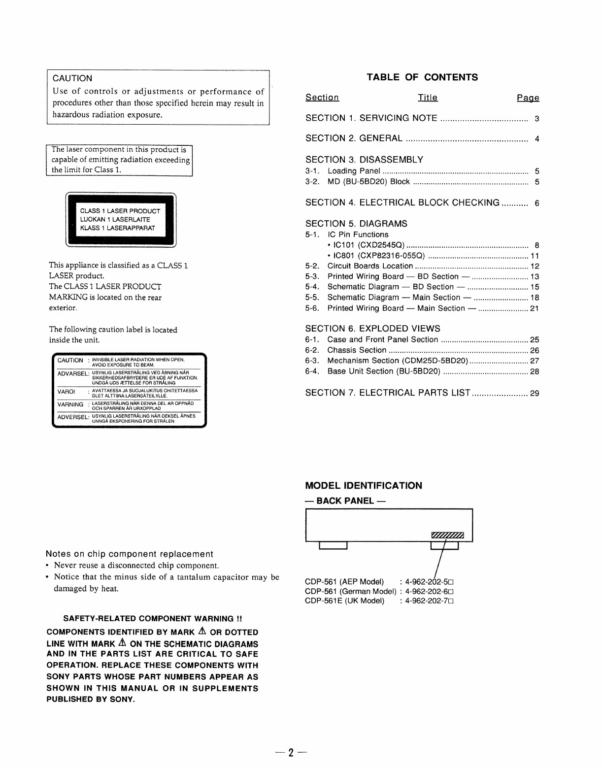
MODEL
IDENTIFICATION
—
BACK
PANEL
—
LLLLLLILL,
CDP-561
(AEP
Model)
:
4-962-202-50
CDP-561
(German
Model)
:
4-962-202-60
CDP-561E
(UK
Model)
:
4-962-202-70


