manuals.online logo
Brands
  1. Home
  2. •
  3. Brands
  4. •
  5. Sony
  6. •
  7. CD Player
  8. •
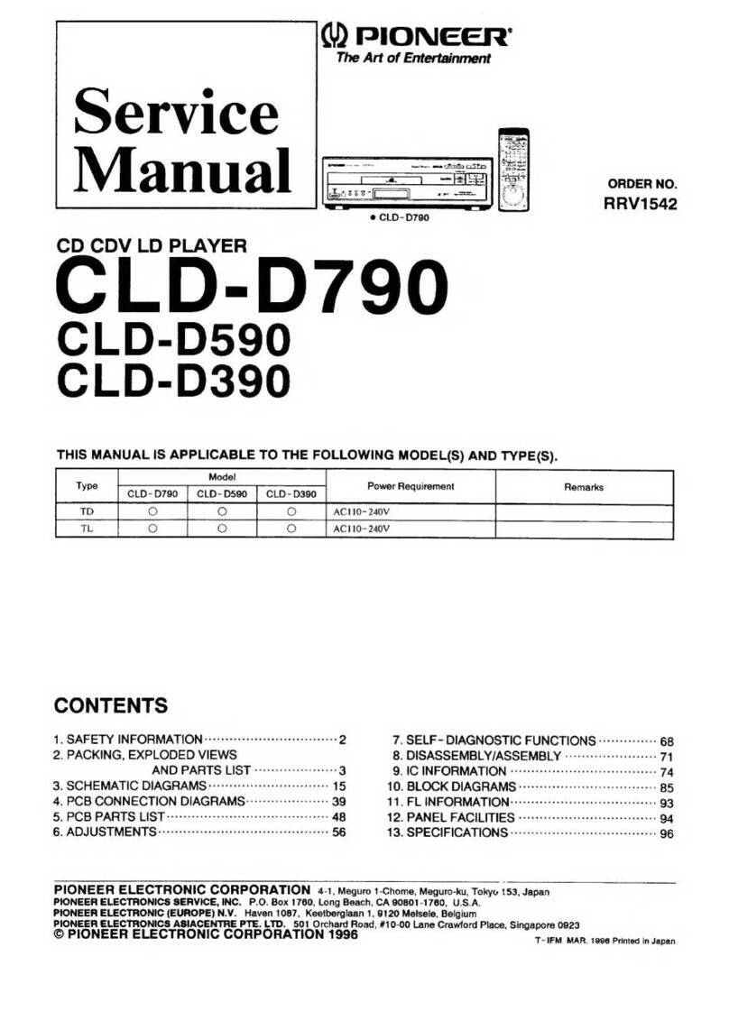
  9. Sony D99 CHASSIS User manual

Sony D99 CHASSIS User manual

CD
section
System
Laser
diode
properties
Spindle
speed
Scan
velocity
Error
correction
D-A
conversion
Frequency
response
Wow
and
flutter
Outputs
(at
9
V
input
level)
“*Measured
by
EIAJ
CP-307
General
Power
requirements
CAUTION
SPECIFICATIONS
Compact
disc
digital
audio
system
Material:
GaAlAs
Wavelength:
780
nm
mission
duration:
Continuous
Laser
output:
Less
than
44.6.W*
*This
output
is
the
value
measured
at
a
distance
of
200
mm
from
the
objective
lens
surface
on
the
Optical
Pick-up
Block.
500
r.p.m.
to
200
r.p.m.
(CLV)
1.2-1.4
m/sec.
Sony
Super
Strategy
Cross
Interleave
Reed
Solomon
Code
{-bit
quarz
time-axis
control
20-20,000
Hz
*2dB
Below
measurable
limit’
*
Line
output
(stereo
minijack)
Output
level
1.0
V
rms
at
50
kilohms
Load
impedance
over
10
kilohms
Headphones
(stereo
minijack)
9mW
+
9
mW
at
16
ohms
Rechargeable
battery
pack
BP-2EX
(supplied)
Battery
case
EBP-2
(supplied)
and
two
size
AA
(LR6)
alkaline
batteries
(optional)
DC
IN
9
V
jack
accepts:
Sony
AC
power
adaptor
(supplied)
-—
Continued
on
page
2
—
Use
of
controls
or
adjustments
or
performance
of
pro-
cedures
other
than
those
specified
herein
may
result
in
hazardous
radiation
exposure,
COMPACT
DI
US
Model
Canadian
Model
AEP
Model
UK
Model
E
Model
DISstmMaN
Model
Name
Using
Similar
Mechanism
|
D-9,//90
CD
Mechanism
Type
CDM-90
D-99
Power
consumption
2.6
W
OC
Dimensions
Weight
Supplied
accessories
Approx.
130.0
x
31.1
x
142.0
mm
(5'/s
x
1"/s
x
5%/s
in.)
(w/h/d)
not
incl.
Inclined
part
(depth),
projecting
parts
and
controls
Approx.
131.0
x
32.4
x
142.7
mm
(51/4
x
15/6
x
55/e
in.)
(w/h/d)
incl.
projecting
parts
and
controls
Approx.
420
g
(15
0z)
not
incl.
rechargeable
battery
Approx.
500
g
(1
Ib
1
02)
incl.
rechargeable
battery
.
AC
power
adaptor
(1),
Battery
case
(1)
Rechargeable
battery
pack
(1),
Carrying
case
(1)
Connecting
cord
(1)
(stereo
minipiug
+
two
phono
plugs)
Stereo
headphones
(1)
Design
and
specifications
subject
to
change
without
notice.
TABLE
OF
CONTENTS
Section
Title
Page
Specifications
POM
ee
mere
e
errr
eee
eee
eee eee
Hee
ee
ene
eee
eeeneeaeeeeHeeseeesereses
1
Ai:
SGP
NER
IN
exhausts
einccuitendinnn
acta
aatraseeeeauccals
2
2
SERVICING
NOTES.
----:-sscccssssccsccscesssccnsecossscevsescenes
3
Befor
Replacing
the
Optical
Block
COOH
EOE
HREOC
HH
EEO
EOOD
3
Note
on
Laser
Diode
Emission
Checkerrrrsrrrrsessersseeseee
4
Laser
Diode
Check
Procedure
OOO
er
ee
eer
eneeeereenreeesereeneees
4
Service
Mode
(service
program)
rere
rrerrrreeererere
rr
Tere
rrr
yy
4
Explanation
of
Terminals
(IC3801
CXD8178Q)-+rreseeerees
5
3.
ELECTRICAL
ADJUSTMENTS
ere
ee
eer
eres
6
4,
DIAGRAMS
4-1,
Block
Diagrams
Cece
e
eee
ew
erro
rer
ne
neene
eee
eeeeeseeeseeeennenee
9
4-2,
PC
Board/Switch/Motor
Layouts
crrrrrereerseeees
11
4-3,
Semiconductor
Lead
Layouts
rerrrsrsesssseseseseeeens
12
4-4,
Printed
Wiring
Boards
Peo
rer
erreverreree
cere
eerreeererene
14
4-5,
Schematic
Diagrams
OEP
ECTeTOEPrErerrererree
ee
er
rer
ee
rr
yy
19
4-6,
Ic
Block
Diagrams
Pomme
ere mee
re
rreeeeerrerereereessseeeeee
22
5.
EXPLODED
VIEWS
Poe eee
ere
eanen
eer
ee
ee
eeeeeeeesereneeeeseeesees
24
6.
ELECTRICAL
PARTS
LIST
Peererre
errr
eee
er
ere
rere
reer
errr
rr
26
SAFETY-RELATED
COMPONENT
WARNING!!
COMPONENTS
IDENTIFIED
BY
MARK
A
OR
DOTTED
LINE
WITH
MARK A\
ON
THE
SCHEMATIC
DIAGRAMS
AND
IN
THE
PARTS
LIST
ARE
CRITICAL
TO
SAFE
OPERATION.
REPLACE
THESE
COMPONENTS
WITH
SONY
PARTS
WHOSE
PART
NUMBERS
APPEAR
AS
SHOWN
IN
THIS
MANUAL
OR
IN
SUPPLEMENTS
PUB-
LISHED
BY
SONY.
SECTION
1
GENERAL
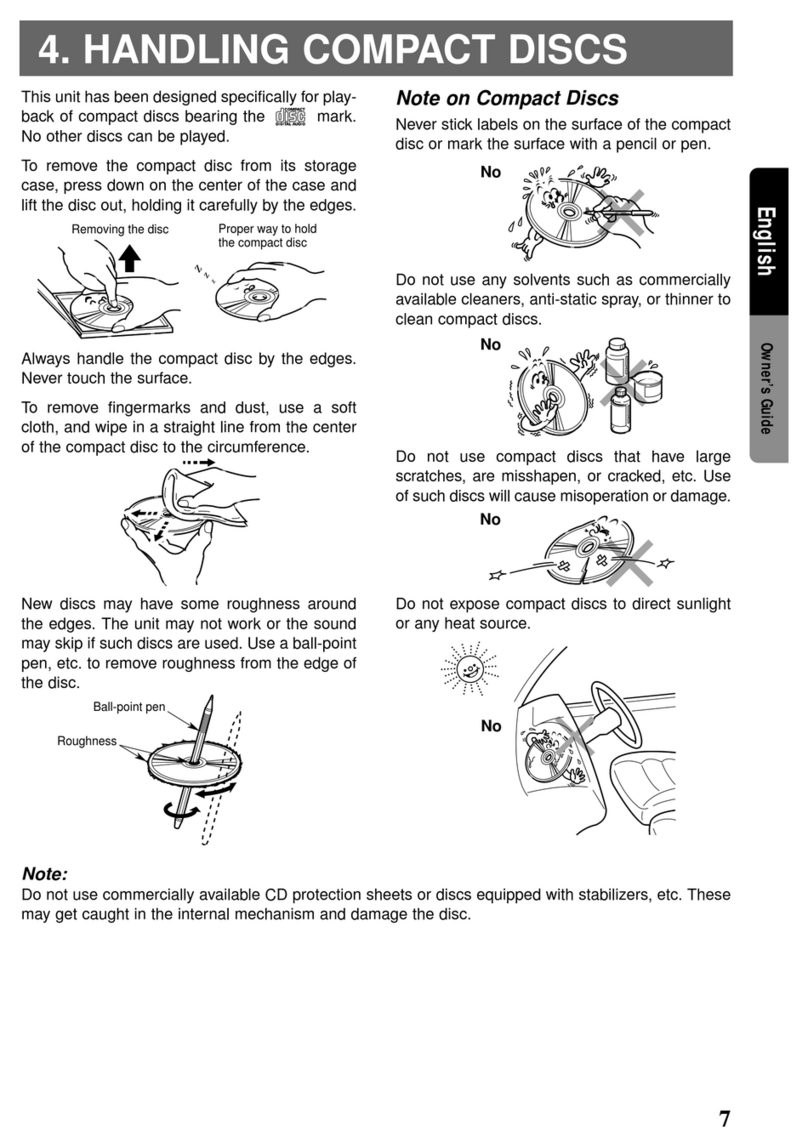
LOCATION
AND
FUNCTION
OF
CONTROLS
Lens
The
laser
beam
is
emitted
from
this
point
to
pick-up
signal
on
the
disc.
PHONES
(headphones)/REMOTE
jack
Disc
window
Display
window
Normally
the
track
number
and
the
elapsed
playing
time
are
shown.
When
the
power
is
supplied’
through
the
DC
IN
9
V
jack,
the
window
will
light
up.
VOLUME
control
(for
listening
headphones)
ENTER/REMAIN
button
HOLD/RESUME
switch
Slide
this
switch
to
its
rightmost
position.
This
locks
the
buttons
to
prevent
them
from
being
acciden-
tally
pressed
(HOLD
function).
To
resume
disc
play
from
the
point
where
you
last
stopped
the
play,
set
the
switch
to
the
right
or
center
position
(RESUME
function).
KEY
MODE
(AMS*/SEARCH/INDEX)
button
PLAY
MODE
button
*
AMS
is
the
abbreviation
of
Auto
Music
Sensor.
ATTENTION
AU
COMPOSANT
AYANT
RAPPORT
A
LA
SECURITE!
LES
COMPOSANTS
IDENTIFIES
PAR
UNE
MARQUE
/\
SUR
LES
DIAGRAMMES
SCHEMATIQUES
ET
LA
LISTE
DES
PIECES
SONT
CRITIQUES
POUR
LA
SECURITE
DE
FONCTIONNEMENT.
NE
REMPLACER
CES
COM-
POSANTS
QUE
PAR
DES
PIECES
SONY
DONT
LES
NUMEROS
SONT
DONNES
DANS
CE
MANUEL
OU
DANS
LES
SUPPLEMENTS
PUBLIES
PAR
SONY.
@
(stop)
button
Ke
mrt
(AMS*/SEARCH/INDEX)
buttons
ml
(play/pause)
button
OPEN
button
REMOTE
jack
Connect
the
optional
remote
control
unit.
LINE
OUT
jack
{stereo
mini
jack)
BASS
BOOST
switch
DC
IN
9
V
jack
(external
power
input)
jack
D-99
SECTION
2
SERVICING
NOTES
NOTES
ON
HANDLING
THE
OPTICAL
PICK-UP
BLOCK
OR
BASE
UNIT
The
laser
diode
in
the
optical
pick-up
block
may
suffer
electrostatic
breakdown
because
of
the
potential
difference
generated
by
the
charged
electrostatic
load,
etc.
on
clothing
and
the
human
body.
During
repair,
pay
attention
to
electrostatic
breakdown
and
also
use
the
procedure
in
the
printed
matter
which
is
included
in
the
repair
parts,
The
flexible
board
is
easily
damaged
and
should
be
handled
with
care,
Before
Replacing
the
Optical
Block
Please
be
sure
to
check
thoroughly
the
parameters
as
par
the
“Optical
Block
Checking
Procedures”
(Part
No.
:
9-960-
027-11)
issued
separately
before
replacing
the
optical
block,
Note
and
specifications
required
to
check
are
given
below.
e
FOK
output
:
IC501@pin
When
checking
FOK,
remove
the
lead
wire
to
spindle
motor
and
unsolder
and
open
IC801@pin
(FOK),
*
S
carve
P-to-P
value
:
3Vp-p
When
checking
S
carve
P-to-P
value,
remove
the
lead
wire
to
spindle
motor,
*
Adjusted
part
for
focus
gain
adjustment
:
RV505
*
RF
signal
P-to-P
value
:
0.7
—
1.25Vp-p
*
Traverse
signal
P-to-P
value:
1.5Vp-p
*
The
repairing
grating
holder
is
impossible,
*
Adjusted
part
for
tracking
gain
adjustment
:
RV501
Flexible
Circuit
Board
Repairing
*
Keep
the
temperature
of
the
soldering
iron
around
270°C
during
repairing,
Do
not
touch
the
soldering
iron
on
the
same
conductor
of
the
circuit
board
(within
3
times),
Be
careful
not
to
apply
force
on
the
conductor
when
soldering
or
unsoldering,
°
Notes
on
chip
component
replacement
*
Never
reuse
a
disconnected
chip
component,
*
Notice
that
the
minus
side
of
a
tantalum
capacitor
may
be
damaged
by
heat,
D-99
NOTES
ON
LASER
DIODE
EMISSION
CHECK
The
laser
beam
on
this
model
is
concentrated
so as
to
be
focused
on
the
disc
reflective
surface
by
the
objective
lens
in
the
Optical
pick-up
block,
Therefore,
when
checking
the
laser
diode
emission,
observe
more
than
30cm
away
from
the
objective
lens,
Laser
Diode
Check
Procedure
The
laser
diode
on
this
set
will
not
emit
unless
the
top
panel
is
closed
and
S901
is
turned
on,
The
laser
diode
will
always
emit
even
if
focus
search
is
not
performed
in
service
mode,
Procedure
1
(service
mode
or
normal
operation)
Check
the
laser
diode
emission
with
the
eye.
1,
Open
top
panel,
2,
Turn
on
S901
in
Fig.
1,
(In
service
mode,
this
operation
is
not
necessary.)
3.
Press
the
Pll
key.
(In
service
mode,
this
operation
is
not
necessary.)
4,
Observe
the
objective
lens
and
confirm
that
the
laser
diode
is
emitting
light,
At
this
time,
the
laser
diode
goes
on
about
10
seconds
due
to
focus
serarch,
Procedure
2
(service
mode
or
normal
operation)
Check
by
the
current
with
flows
in
the
laser
diode,
1,
Close
the
top
panel.
2.
Remove
the
main
board
and
read
the
current
value
on
the
label
affixed
to
the
Optical
pick-up
block,
(Label
on
Optical
pick-up
block)
KSS—220A
JAPAN
$123
546
current
value
This
means
54.6mA,
3.
Connect
a
VOM
to
TPl
and
TP2
(both
side
of
R510:
10Q)
.
Press
the
Dil
key.
.
Calculate
the
current
by
the
VOM
reading,
VOM
reading
(V)
+resistance
of
R510=current
(A)
ex,
VOM
reading=0,56V
0,56+10=0,056
(A)
=56
(mA)
6.
Confirm
that
the
ammeter
reading
is
within
the
range
given
below,
value
on
labelt#,;mA
(25°C)
variation
relative
to
temperature
:0.4mA//°C
(Current
increases
when
temperature
rises
and
decreases
when
it
drops.)
or
&
SERVICE
MODE
(service
program)
*Step
1
(Service
Mode
setting
method)
1,
Turn
the
HOLD
switch
to
OFF
with
the
external
power
supply
not
plugged
in
(no
power
applied
to
set),
2.
Press
the
Dll
key.
3.
Solder
jumper
TEST
terminal,
(IC801
pin@
BAT-E
is
grounded.)
4,
Plug
in
external
power
supply.
This
puts
the
set
into
service
mode,
*Step
2
(Service
Mode
operation)
1,
When
service
mode
is
set,
the
display
will
change
6
times,
and
those
6
changes
will
be
repeated
over
and
over,
Even
if
LCD
dose
not
display,
other
operations
will
be
performed,
2,
When
Dp
or
Kd
key
is
pressed,
the
optical
pick-up
block
moves
to
the
inside
or
outside
circumference,
Tracking
servo
and
sled
servo
go
off
when
this
is
done,
so
press
KEY-MODE
to
turn
on
the
tracking
servo
if
necessary.
3.
When
REMAIN
is
pressed,
the
display
stops,
When
REMAIN
is
released,
the
display
continues
to
change.
This
allows
check
of
each
segment,
4,
When
}>lIl
Key
is
pressed,
CLV-S
(pull-in
mode)
starts
while
performing
focus
search,
When
there
is
no
disc
installed,
focus
search
is
repeated
with
rotating
disc
motor,
5,
When
KEY-MODE
is
pressed,
tracking
servo,
sled
servo
and
CLV-A
(servo
during
PLAY)
go
ON,
6.
When
4
and
5
are
performed,
the
disc
begins
to
play.
At
this
time,
the
top
panel
should
be
closed
and
S901
are
to
be
ON,
A
sound
is
not
produced
as
muting
is
ON,
7,
All
servo
(focus,
tracking,
sled
and
spindle)
go
off
when
Mikey
is
pressed.
Disc
motor
rotate
by
inertia
for
a
some
time,
Cay,
$901
(OPEN,“CLOSE
switch)
PPI
Fr)
Optical
pick-up
block
goes
to
outside
circumference
goes
to
inside
(display
stop)
circumference
(FR)
[see
pick-up
a
REMAIN
W@
(STOP)
)
(servo
all
off]
KEY-MODE
Cee
servo
and
sled
servo
on
p>
II
(PLAY/PAUSE)
%
Be
sure
to
keep
HOLD
FOCUS
on
and
CLV-S
switch
OFF.|f
not,
the
set
(
mode
(RUN-UP
mode)
sie)
cannot
receive
the
input
from
each
keys.
Fig.1
*Step
3
(Service
Mode
release)
1,
First
be
sure
to
unplug
the
external
power
supply.
2,
Then
remove
the
solder
jumper
TEST
terminal,
3,
The
set
will
now
operated
normally,
—
4
—
D-99
@
Explanation
of
terminals
(IC301
CXD8178Q)
Terminal
No.
|Name
of
terminal
MLD
RSTB
Descriptions
Micro
computer
command
load
input
(When
L,
load)
Reset
terminal
(L
:
reset)
When
L:
Signal
processing
LSI
format
When
H:
FS
format
|
E
TP1
Digital
filter
part
test
output
terminal
1
TEST
1
Test
signal
input
terminal
1
for
digital
filter
part
inspection
Normal:
”L.”
Digital
filter
part
test
output
terminal
2
TEST
2
Test
signal
input
terminal
2
for
digital
filter
part
inspection
Normal:
”L”
Zz
o}
oe)
10
11
12
13
14
15
AVop4
OUTL
(-)
AVss4
AVss3
OUTL
(+)
AVo03
NC
AVoo2
OUTR
(+)
AVss2
AVss1
OUTER
<=)
AVop1
DVoo1
DVss1
Analog
system
power
terminal
4
(+3.9V)
L
ch
opposite
phase
PWM
output
terminal
Analog
system
ground
terminal
4.
Analog
system
ground
terminal
3
L.
ch
normal
phase
PWM
output
terminal
Analog
system
power
terminal
3
(+3.9V)
17
18
19
0
21
22
3
4
Analog
system
power
terminal
2
(+3.9V)
R
ch
normal
phase
PWM
output
terminal
Analog
system
ground
terminal
2
NO
Analog
system
ground
terminal
1
R
ch
opposite
phase
PWM
output
terminal
Analog
system
power
terminal
1
(+3.9V)
Nn
Digital
system
power
terminal
1
(Power
for
oscillator)
NO
Digital
system
ground
terminal
1
(Ground
for
oscillator)
N
ol
Crystal
oscillator
terminal
we)
(o>)
Crystal
oscillator
terminal
(Outer
clock
input
terminal)
Ph
N
~j
28
)
30
DVoo2
Digital
system
power
terminal
2
(+3.9V)
DVss2
NSUB
ZFLGB
192FS
LRPOL
Digital
system
ground
terminal
2
Connect
to
D-VDD
(Silicon
circuit
board
electric
potential
fixing
terminal)
W
Zero
input
inspection
output
terminal
(When
zero
inspection
:
L)
192FS
(=8.4672MHz)
output
terminal
LRCLK
polarity
selection
input
terminal
LRCLK
input
terminal
When
LR-POL
H,
H:
L
ch
data
input
»
L:R
ch
data
input
When
LR-POL
L,
L:
L
ch
data
input>H:R
ch
data
input
WwW
2
33
ie)
34
LRCLK
35
6
BCLK
SRDATA
DVss3
DVpp
Digital
system
ground
terminal
(COM
electric
potential
fixing
terminal)
(+3.9V)
384FS
384FS
(=16.9344MHz)
output
terminal
Power
down
terminal
(H
:
power
down
mode)
Serial
input
bit
clock
W
Serial
input
data
(digital)
input
terminal
3
Digital
system
ground
terminal
3
W
8
)
hl]
@w
oO
MDATA
MCLK
4
—
Micro
computer
command
data
input
terminal
2
Clock
input
terminal
for
micro
computer
command
D-99
SECTION
3
ELECTRICAL
ADJUSTMENTS
Notes
on
Adjustment
1,
Perform
adjustments
except
for
BATTERY
REMAINS
ADJUSTMENT
in
service
mode,
Be
sure
to
release
service
mode
after
completing
adjustment,
(Refer
to
“Service
Mode
(service
program)”
on
page
4,)
2,
Perform adjustments
in
the
order
given,
3.
Use
YEDS-18
disc
(part
No,
:
3-702-101-01)
only
indicated,
4,
Power
supply
voltage:
DC
9V
HOLD
switch
:
OFF
VOLUME
knob:
MIN
PREPARATION
Put
the
set
into
service
mode
(See
page
4.)
and
perform
the
following
checks,
*
Sled
Motor
Check
1,
Press
the
OPEN
button
and
open
the
top
panel.
2.
Press
the
>Wl,l4
keys
and
make
sure
that
the
optical
pick-up
block
moves
smoothly,
without
catching,
from
the
inmost—~outmost—inmost
circumference,
>I:
UPF
moves
outward
K4:
UPF
moves
inward
*Focus
Search
Check
1,
Press
the
OPEN
button
and
open
the
top
panel.
2,
Press
thed{l
key.
(Focus
search
is
performed
continuously.)
3.
Observe
the
UPF
objective
lens
and
check
that
it
moves
smoothly
up
and
down
with
no
catching
or
noises.
4.
Press
the
MM
key.
Check
that
focus
search
operation
stops,
If
it
does
not,
press
the
Mf
key
again.
Battery
Remains
Indication
Adjustment
Adjustment
procedure:
VOM
(DC
range)
main
board
TP3
(VREF)
TP4
(IC802@)
1,
Apply
DC
3.5V
both
side
of
battery
terminal,
2,
Insert
the
disc
(YEDS-18)
and
press
the
bllkey.
3.
Adjust
RV801
so
that
the
voltage
of
TP4
(IC802dD)
is
the
same
as
TP3
(V
REF),
+3,.9V
Adjustment
Adjustment
Procedure
:
1,
Put
the
set
into
STOP
state
service
mode
(see
page
4),
2.
Connect
the
VOM
to
main
board
test
point
TP(+3.9V).
3.
Adjust
RV401
for
3.95V-4V
reading
on
the
VOM.
4,
After
adjustment,
release
service
mode
(see
page4),
+3.4V
Adjustment
Adjustment
Procedure
:
1.
Put
the
set
into
STOP
state
service
mode
(see
page4).
Connect
the
VOM
to
main
board
test
point
TP
(+3,4V).
Adjust
RV402
for
3.45V
to
3.5V
on
the
VOM
reading,
After
adjustment,
release
service
mode
(see
page
4),
+3.6V
Adjustment
Adjustment
Procedure
:
1,
Apply
DC
3V
both
side
of
battery
terminal,
2.
Connect
the
VOM
to
main
board
test
point
TP7
(collector
of
Q487).
Insert
the
disc
(YEDS-18)
and
close
the
top
panel.
Press
the
Dll
key.
Adjust
RV450
for
3.65V
to
3.7V
on
the
VOM
reading.
PLL
Free
Run
Frequency
Check
and
Adjustment
Check/“Adjustment
Procedure
:
=
WON
a w
frequency
counter
TP
(PLCK)
~t,-—
p=
1,
Disconnect
EFM
solder
jumper
terminal
on
the
main
board,
2,
Connect
a
frequency
counter
to
main
board
test
point
TP8(IC601
@).
3.
Put
the
set
into
service
mode
(See
page
4),
4,
Check
that
the
frequency
counter
reading
is
4,35+0,01
MHz.
If
not,
adjust
RV504
so
that
it
is
4,85+0,01MHz,
After
adjustment,
release
service
mode
(see
page4),
6.
Short
the
jumper
terminal
disconnected
in
step
1,
main
board
ol
Tracking
Balance
Adjustment
Conditions
:
The
set
should
be
placed
either
horizontally.
Adjustment
Procedure
:
oscilloscpe
(DC_range)
main
board
———
TP9
(TE)
vc
Connect
the
oscilloscope
to
main
board
TP9
(IC501@).
Put
the
set
into
service
mode
(See
page
4.)
Press
the
>|
and
Ké4
keys
to
move
the
UPF
to
the
center,
Insert
the
disc
(YEDS-18)
and
close
the
top
panel.
Press
the
Dil
key.
It
will
go
from
focus
search
to
focus
on,
and
CLV
OU
AE
on
pull-in
mode
state,
Tracking
and
sled
are
OFF,
6.
Adjust
RV502
so
that
the
oscilloscope
wavaform
is
symmetrical
on
the
top
and
bottom
in
relation
to
OV.
time
as
lon
ossible
to
obtain
best
wave-
Note
:
Take
swee
as
form.
A
A
1-2Vpp
OV
.
OV
B
|
A=B
Bose
7,
-Unplug
the
external
power
supply
to
stop
spindle
motor
from
rotating.
8.
After
adjustment,
release
service
mode
(see
page4).
Focus
Bias
Adjustment
Conditions
:
The
set
should
be
placed
either
horizontally.
Adjustment
Procedure
:
oscilloscope
oscilloscope
(DC
range)
main
board
(DC
range)
main
board
ye
aati
\ca0e
fae
TP10
i
a
a
ad
TP11
(FE)
“T+
ve
—__—_———o
-
ve
-
1.
Put
the
set
into
STOP
state
in
service
mode
(See
page
4),
2.
Connect
the
oscilloscope
to
main
board
test
point
TP10(CIC501@).
3.
Press
the
bl
and
Kd
key
to
move
the
UPF
to
the
center,
(Move
the
UPF
to
the
music
area
on
the
disc
to
enable
easy
visibility
of
the
eye
pattern).
4,
Insert
the
disc
(YEDS-18)
and
close
the
top
panel,
Press
the
Pll
key.
or
D-99
6.
Press
the
KEY-MODE
button.
7,
Adjust
RV503
so
that
the
oscilloscope
waveform
eye
pattern
is
good,
A
good
eye
pattern
means
that
the
diamond
shape
(©)
in
the
center
of
the
waveform
can
be
clearly
distinguished,
*RF
Signal
Reference
Waveform
(eye
pattern)
VOLT
/DIV
:
200mV
TIME/DIV
:
500nS
Nain
RANMA
:
Wy
"
O
WV
WY
44
RF
level
AYN
|
0,85-1,35V
NN
ue
When
observing
the
eye
pattern,
set
the
oscilloscope
for
AC
range
and
raise
vertical
sensitivity.
8.
Read
the
voltage
on
TP1l1
(1C502@),
+20mV
to
50mV
Adjust
RV503
again
for
+50mV
reading
on
oscilloscope,
+20mV
to
—20mV
Adjust
RV503
again
for
—20mV
reading
on
oscilloscope,
9,
Unplug
the
external
power
supply
to
stop
spindle
motor
from
rotating.
Adjust
RV503
again
refering
to
the
table
followed.
10.
After
adjustment,
release
service
mode
(see
page
4).
Adjustment
Parts
Location
Diagram
RV801
(Battery
Remains
Indication
Adjustment
(MAIN
BOARD)
—SIDE
A-—
RV450
RV401
+3,6V
Adjustment
(+3,9V
Adjustment)
(
sustnent)
RV402
(+3.4V
Adjustment)
{
}1C503
ves
L_]
1C801
©
16301
RV501
;
(Tracking
Gain
Adjustment)
RV502
(Tracking
Balance
Adjustment)
RV505
.
(Focus
Gain
Adjustment)
03
(Focus
Bias
Adjustment)
RV504
(PLL
Free
Run
Frequency
Check
and
Adjustment)
D-99
Reference
.
CD
jig
connection
:
Focus
Tracking
Gain
Adjustment
Remove
the
solder
jumpers
at
the
TE
and
FE
locations
and
On
this
set,
it
is
very
difficult
to
simplify
this
adjust-
connect
the
CD
jig,
ment,
The
adjustment
procedure
is
described
in
the
separate
CD
A
frequency
responce
analyzer
or
CD
jig
is
necessary
jig
Instruction
Manual,
in
order
to
perform
this
adjustment
exactly,
However,
this
gain
has
a
margin,
so
even
if
it
is
slightly
off,
there
is
no
problem.
Therefore,
do
not
perfrom
this
adjustment,
Focus/
tracking
gain
determines
the
pick-up
followup
(vertical
and
horizontal)
relative
to
mechanical
noise
and
mechanical
shock
when
the
2-axis
device
operate,
*
When
gain
is
high,
the
noise
when
the
2-axis
device
operates
increases,
*
When
gain
is
low,
it
is
more
susceptible
to
mechanical
shock
and
skipping
occurs
more
easily,
,
However,
as
these
reciprocate,
the
adjustment
is
at
the
point
where
both
are
satisfied,
This
adjustment
is
to
be
performed
with
using
when
replacing
the
following
parts:
*
UPF
(optical
pick-up
block)
Adjustment
Parts
Location
Diagram
*
RVSO1
(tracking
gain
volume)
(MAIN
BOARD)
—SIDE
A—
*
RV505
(focus
gain
volume)
cP
RNS
02
22K
(B)
J801
=
CD
jig
-
Fig.3
4-1,
BLOCK
DIAGRAMS
1c501
RF
_AMP/SIGNAL
PROCESSER
OPTICAL
PICK-UP
BLOCK.
i
KSS~220A
1C303
$30!
DBB
HEADPHONE
AMP
OBB
MAX
q
(5).
PNF
MID
<J
w
([R
qj
(13)
R
OUT
0)
L.
OUT
§302(2/2)
friones)
RV30I-1
MUTING
Qi02
RCH
J30i
°
LINE
OUT
l
Neen
MUTING
Qi01
7
SECTION
4
DIAGRAMS
RV505
RV501
16301
D
MUT
DE
EMPHASIS
ala
EMPHASIS
SW
142
0302
+3.4V
——
IC502
FOCUS,
TRACKING,
SLED/CLV
SERVO
Qs03
‘8
ERROR
DET
7A
CONVERTER
ING
Q604(1/2)
“)
fn
Q502
Q605
CLV
SWITCH
G8)
(y
(-
oom
H€
+8
(1C301)
iC45'
0
PWM
POWER
SUPPLY
nN
oO
S
@)
Vv
CONT
Q450,Q452
<
Na
>
°o
@)
(veer
(&)
ON/OFF
SWITCH
Q453
SWITCH
Q462,463
OSs
P
OMnsebd”®
+3.4V
Vv
REG
Q407
V
REG
Q430,0416
SWITCH
Q416
D408
CONV CONV
hd
REG
CONT
REG
CONT
Q406
Q405
Q461
Q464
|
Pioas
D459
SWITCH
SWITCH SWITCH
V
REG
V
REG
SWITCH
Q451
Q456
Q457
|
|
Q4I7
Q431
Q409
4!
_
a
ons
V_
REG
Q4i8
BP-2
aL
BATT
1C504
PWM
D
Dc-DC
RIVERS
CONVERTER
FOCUS
COIL
=)
TRACKING
coil
M901
SPINDL
MOTOR
M902
SLED
MOTOR
0417
oe
@)
CONVERTER
3404
@
SWITCH
T
Q801
z
1¢601
DIGITAL
SIGNAL
PROCESSER
1_|
iC802
RIPPLE
FILTER
0304,
305
|
V
DET
Qs0s
08isS
>
|
>
VOL
CONTROL
V
DET
Q427~429
Q420
+3.4V
V
DET
Q811
BATT
LEVEL
DET
a
p>
D803
ao
SWITCH
Q806
MUTE
Q807
SWITCH
0426
PLAY
hy
Mone
—O
oO
KEY
J302(1/2)
MODE
PHONES
oh
pp
OO
$808-|
ae,
|
+
Oo
oO—
[HOLD]
ON
OFF
oO
1
*
aL
>t
Oo
O-
L
oS
REMAIN
ial
vop
68)
(1)
DIRECTION
24
(5)
sack
A
(2)
LATCH
(6)
DATA
6s
r
SWITCH
Q803
ND801
tcp
1¢801
SYSTEM
CONTROL
XTAL
(0)
(5)
sToP
EXTAL
@1)
(9)
K
REM
S$
DOOR
(21)
RESET
1€804,Q809
me
x3801
$901
Y
SWiTCH
aso4
B+
D816~821
tq
82
LCO
BACK
LIGHT
J801
TS
42.
PC
BOARD“SWITCH
MOTOR
LAYOUTS
LDC
module
(ND801)
main
board
door
switch
($901)
HOLD
switch
contorol
board
(S808)
optical
pick-up
block
CUPF)
KSS-220A
sled
motor
(M902)
limit
switch
($902)
spindle
motor
(M901)
e
LCD
MODULE
COMMON
He
eee
LLA
a
SHUEELE
$e
BA
PALA
——
FA
EE
i
TEE
BH
SRE
5
’aunP
ann
ann
ammtann
ane
aen
oe
ee
1234567
9
12
3:0
COM
.
SEG
SEGMENT
4-3.
SEMICONDUCTOR
LEAD
LAYOUTS
BA3818F-SY
—
NJM2100M
765
1234
(TOP
virw)
RH5RC351A
1.V
OuT
2
VIN
3.GNO
TC4S11F
TC7SO4F
DTA124EK
DTA143TK
DTA144TK
DTC124EK
DTC124TK
DTC143TK
DTC144WK
2SA1037K
2SA1162
2SB1197K
2$D1048X7
2S8D1781K
FMS1
2SB1182F5
2SD1758F5-R
Cc
a
2SB798-DL
cathode
MA152WK
SLM-125YW-C1
cathode
enode
DAN204K
MA157
RB471E
!
2
3
RB411D
RB420D
RD4.7M
RD5.6M
RD7.5M
RD8.2M
RD12M
SBQ5-05CP
$B01-O5CP
RB110C
$B10-O5PCP
|
‘D-99
44.
PRINTED
WIRING
BOARDS
¢
See
page
12
for.
Semiconductor
Lead
Layouts.
es
Oe
OE
el
a
i
A
A
ee
Nae
OP
a
ON
A
OO
I
OO
le
6
-3>—_________—
¢
SEMICONDUCTOR
LOCATION
[et
Nox
[
cosnion
J
Pot
No.
|
Uosoton
[Pat
Ne
[
Loto
|
$802
$801
$806 $807
(MAIN
BOARD
(SIDE
A)]
{MAIN
BOARD
(SIDE
B))
{TK
BOARD]
BP-2
RECHARGEABLE
EBP-2
BATTERY
CASE
ORY
BATTERY
SIZE"’AA"
VEC
DESIGNATION
Ré)
2PCS,3V
{CONTROL
BOARD
(SIDE
A)]
O-eO
[CONTROL
BOARD
(SIDE
8))
——
ssid
ea
PATTIE
$808
=I
-2
HOLD
RESUME]
OF
F~ONe-ON
OPTICAL
PICK-UP
BLOCK
KSS-
220A
$902
LIMIT
SWITCH
Gang
REACHES’
INNER
POSITION
SPINDLE
MOTOR
*
O-~:
parts
extracted
from
the
component
side.
+
@—-:
parts
extracted
from
the
conductor
side.
*
MM:
parts
mounted
on
the
conductor
side.
:
Through
hole.
*
:
Pattern
on
the
side
which
is
seen.
M902
SLED
MOTOR
°
$301
OBB-NORM
=
MID-~MAX
—<“r>
:
Pattern
of
the
rear
side.
ee
ee
ee
ee
—
14—
—/S—
a
da
=
Note:
‘
2
>
B+
Line
°
|
:
adjustment
for
repair.
*
All
capacitors
are
in
uF
unless
otherwise
noted.
pF:
»
uF
«
Voltages
and
wavefrorms
current
are
measured
with
top
5OQWV
or
less
are
not
indicated
except
for
electrolytics
panel
closed
and
tantalums.
*
Power
voltage
is
dc
QV
and
fed
with
regulated
de
power
*
All
resistors
are
in
2
and
%W
or
less
unless
otherwise
supply
from
external
power
voltage
jack.
specified.
¢
Voltage
and
waveforms
are
de
with
respect
to
ground
+
%
:
indicates
tolerance.
in
service
mode.
>
A
:
internal
component.
no
mark
:
play
¢
):
play
(Battery
operation)
Note:
Note:
;
i
As
Baie
Ae:
Ge:
es
Ge
sont
elles
*
Voltages
are
taken
with
a
VOM
(Input
impedance
10M
Q),
ted
line
with
mark
pour
la
sécurité.
Voltage
variations
may
be
noted
due
to
normal
produc-
are
critical
for
safety.
Ne
les
remplacer
que
par
une
tion
tolerances.
Reece
eee.
Part
raid
portent
le
numero
speck:
-
Waveforms
are
taken
with
a
oscilloscope.
«
See
page
4
for
setup
of
service
mode.
a
Signal
path.
wz
:CD
1
2
3
4
5 6
7
8
a8
10
11
12
13
14
15 16 17
18
19
20
45.
SCHEMATIC
DIAGRAMS_
°*
See
page
22
for
IC
Block
Diagrams.
CDM-90
(2/2)
:
-—
-
—-
Or
Oe
OO OO
OO
OPTICAL
(MAIN
BOARD]
i
:
ae
ie
PICK-UP
BLOCK
AUTOMATIC
FRAN:
#
Bla
mle
ensoz
4p
|
KSS-2202
2
2
i
BLK
:
‘
POWER
CONTROL
AN
g
Ea
8
oe|
fale
Lee
Fe"
[Focus
cow
|
Treg
R510
10
TB!
NOOR
£
REST
2.2K
2|
|
tt
a
i
WWW
1.7
a
|
|
2.6
3
T-
'
9501
|s2VP=P
ts
1.8
is
Hea
!
4
xnk60s
ae
:
7
Le
KING
h
3.
e540
AS3I
g
RS50
+
TRACKI
|
5
2
o*
NT
osag:
ceso
|
033
2
Beak
|
Cot
|
2.0.
6}
[3
Few
3
F
N,
i+
:
CDM-90
|
502
.505
334
RS30
sale
RVS04
0-44
ry
-
’
|
i
RV502
9504
RBS200
"3.5
|
Q502
,
5533
BS50
9537
|
cog
[PLL]
;
YEREVAN
NAYAS
te
:
(1/2)
TRACKING
CLV
SWITCH
RS
Coes
Lass
#Roee
0:5N
|
0.047
EMERALD
SEEDS
|
|
—————
BALANCE
¢
(SPINDL
MOTOR)
iG
ago
Fe
TOcee
2
56)
=
amcoaees
exes
ep
ca58
:
KS5-220A
172
‘
pI
C512
oda
Tor
Tate)
C546,
LEEEF
SSEESE
0
18y
|
[4
oes,
=
BLK
'
RV502
22k
1.2]
18]1.8/1-81.8]1.8
10.2,
33%
33°6.3V
csit
1
C532.
RVSOS
3.6
1.5
TOV
TA
a5uu
&
Gus
2
a
iTA
'
‘A
!
i
+
Bde
Le
de
ae
RSSS
2.
2k
1p
100de
BY
R529
3.9K
0.5m)
IK
PWM
POWER
SUPPLY
0450
,
452.455
—H
INI
2
=
SH
INKE)—
|
i
;
24K
23K
22K
21X20
KISX
18K
17
St
:
VOLTAGE
CONTROL
5
©
es
|
|
H ‘
A 2
iy
Lack
{
2
(BATT:
ON)
ar
HOUTA
HOUTSAS)
OS
L505
:
‘
' ‘
wn
1
S
‘
L
‘co
|
aME
ow
lal
setegges™
|
|
ae
oe
oe
Haim
Gru
re
ec
r
ae
i
O14
‘
8
=
R507
R508)
LRSNS
HON
|
1.813,6)2.
[3.6
81.8]
1.8
“cuk
q
WN
INT2
IC504
VINSHSEO
;
‘
nae
i
|
“|i
Qs)
Et
P/N
(16)
ISK
6.2K)
a
‘alates
age
R450,
220K
we
te,
4
oth
fide
“FL
IN2
a
FL
INA(3)—
Tavent
|]
SA62
|
SPINDLE
|
A
‘
Si
643
7%)
VR
RF
(15
rset
|
15
505
BY
SSY
SAY
SRY
SVB
Y
BOY
1912827
(26X25
8
x
Os
Fes
3
eS2
ra}
aN
wPelaiseu
=
SNA
yt
6o3y
SP+
H
i
|
KI]
dé
o5is
ol?
=
[LogsyoR|
hicbal
may
i
pancet
ge
450
=
7a
haat
eae
o.3y
i
Shad
oe
PWM
oRivers
PMR
ONOSAZ
ETS
TA
+
|
|
‘
+
7
7
if
9.01
G7)"
BL
og
RFO
(14
a
7
7
ae
|
2>Zaé¢eru
r\-\z
ow
~
+22
(18)
|
9
Is
os
RV450
STA
“HOUT
2A
OC/DC
CONVERTER
HOUT4AGR
:
"
a
{
RV503
“C02
}eso1
2.4-RET'CB
S09
|
9505
C538
3.4
veSFtss
3
a\e
6D
3.6
1
in
=
3.6V
ADJ
+
HOINSCS
0.6
10
|
—
|
F
8
Id
CXA12710
cs10
|
39
I35
DTC124EK
t
csa7)
4
jAQ0Oms
—
c)
:
452
OTS
mB
|
27)
oH
IN2
‘
0
¥
10¥
sp-
_
wgot
|
;
FOCUS
pai
29)°CC1
re
amp
|'8Ne
(12
0.0471
7%,
7
10906
37)
VCC
2.3
XLT
(2%
{
1060.
“
als
RQ
yeic
L457
«
HOUT
2B
HOUTSHS
:
:
|
oh
48
ps
356.3
a
“VEE
SIGNAL
vec
(iaesS
A536
36)
SPAL©
2.4
DATA
(28
zs
oATA
)
]
|
Meee
fo
%
gph
}
{|=
=
ayo
oral
|
|
+.
:
La
10
1.7
PROCESSER
._
R505
180k,
*
|
2
120k
i
1.8
:
43.4
XRST
4
7
B
w
{
=
s)VOUT
@
PCR
es
Hote
ie}
:
tos
nygos_
sFEBIAS
Cone
Ow
j
39)
SPOLO
xRST
(22
I
ust
ES
=
455
=
nto
z
-
SYNC(SS
0807
i
|
Pat
{ii
47%
2
18
1
aoe
2.0*
R554
Ik
.
(05)|
—
2satTaa
°
=PT
0.7
Slat
4
Gg
2
ROI2M,
0506
1
SL
|
i
:
wale
tr2
RSO1
100
32)
FE
Go
bg
FOK
(3)y83,.4
|
ashi
a7k
40)
LRCK
Votator-
BIRC
QUST
S
VEXISKUNINUZN
OAS
=
=(o
e
28
Pea
ANZ202K
Sats
1
3}
MOTOR}
|
7
w
&
a
en
Fa
aE
j
s)
FOK
COUT.
Oar
(1.4)
(t)
abt
idc
z
&ea\2FSeS98sa
RbIeM
|
+
|
WwW
‘
.
Fax
0/0/6
«
wu
C506
34°
(3)
MIRR
1c502
AVEE
(13
]
:
1¢450
o
\
ae
|
ar
ot
J
cxat2720
CER!
SENSE
FATO16N
%
BEGGBCO000086
;
©
ij
i
l
LODOCKONE
8)
SVEE
FOCUS/TRACKING/
SENS
(1)
(0.6)
oe
Cato
:
:
caciad
d
sl
BI
ifs
c
62
|
_
“Y’wsoa!
q
q
.
w
oa
L>)
L
|
’
pope
1.6]
6]
6
Tebae
“2a
R50!
SOC
ar
ET
FSET
USo8
TYTYSXOYGXOYT
XG
0452
Fk
—9
6.3
z
5°48 $55%
real
|=
3
fof
Logon
Re
|
|
ane
Pas
|
-
EFM
45)
TE
sstop
(1)\—
R525_10k
ae
2901963
Th
=
a
PH
pag
|
=
s
|
oe
:
ae
—
RVSO!
R502
C305
2700
SL
oat
|
180%
26
SLO
(228
1
Tosa
|
Pots
o
cele
aya
ch
aset
Le
|B
&
css6
|
|
OPTICAL
PICK-UP
BLOCK
oi]
590
:
esd
1.8
suo
fie]
Lose
fags
yh
|
Fras
#98
ne
TRACING
|||
coe
Re
75k
cs03
2-46,
|
cso
Ait)
arse
slo
(ie
a3,
=
Or
7
220
TOV
|
15k
A
|
|
Has
¢
L_SAIN
Ae
She
{|
ore
|
2X
Re,
SED
Fe
1.8
ig
1818
sk
@
G—
df
:
“*
:
|
im)
amas]!
S
alg/so
2205
SL
ey
2
|
|
,
—
ee
ASY
goercee
s
ez zx
Be
“4
6.3V
peer
RV505
=
Vee
C507
33
6.3V
ig
R522
Th
mth
'
al
|
,
“QRRMGE-6v
[Focus
g
R504
10k
|
csaol
|
$958
TYAEXIXE
XENIA
XX?
100k
018.6)
|
APROX.|OOmVp-p
-
LGAIN
=
sar
|
us
lS
a
Qari
oe
Ls
|
fe
Fe
ga02|
:
=|
|
:
f3a3
(505
(17;
|
'
Ls
;
BENG
=
5
2F
Tbe
5R0
0(3)
9487
[2Siifee
a.6l
oS
eB
|
T7804
A
feos
*
Lets}
Ole)
{
ee
ces
eee
ee
a]
ss
&
;
if
C505]
|
5
il
a
ee
—
‘
rel
83
a7)
ore
40
easel
dy
(BATON)
|
Mh
er
Be
ss
2
7S
Si
INVERTER
-
ine
7
a
7
JR504LA
1.6
\
iTA
-
;
Asp
:
|
a
woe
.
£0
(BATT
ON)
MA
42k
|
Gi
&
ree
APROX.
500
mVp-p
:
0563
cases
Ls
3.5
BS
ae
ae
J
oe
¥LoTP3
aeasto
abetho
|
L452
'
LIMIT
SWITCH
BSL
|180e
FRAT
YD YG
SAS
2
3
5
feos
|
584?
BQ
4,2
;
Me
ON:
UPF_REACHES
:
ao
2m
s
Sop
4.7
[3.5
R52
asi
Foe
ee
R445
680
INNER
POSITION
ti
i
:
c539
w”,
6
on
R518
#TA
C5244,
C526
RENZ00
9
adbries
4.6
Q405
,406
Fe,
|
LEEOS
oa
RS
RS14
rs
ae)
rd
BS
ut
HGS
ey
0.22
eas
R4sg
er
3
age
q
0C-DC
‘
re
“gar
A
NJMZ1004
HEP
Ay
330K
FNG4
3
shy
SF
V0K
avaol
[E55]
ik
ES
REG
SWITCH
g
z
eee
eny
i
a
eens
5
‘
a
:
¢|iP?
=
Pais
nr
diel
|
0454
eS
-
2shitast.2|
7
Se
4.6
OTCI24EK
AVCC
5
=
:
:
-
:
S&
4.
oer
Agl4
rail
4.6
L_046t
2981
197K
:
“toe
-
se
[y]
poze,
2407,
408,422
an
,
Lasat
tar
4g
‘402
i
ee
|
IC503
9503
,
504
ES
sea
2)
Fai
|
Rais
sngor
Rbstio
aN
39
|
egtehy
eda
Xu
-
tk
‘
REG
CONTROL
!
MDS
AMP
1501
TRACKING
,
FOCUS
:
$~
=
Rags
(BATT
:ON)
0.7
FY
TQeH
ERROR
DET
5.0V
F
3
gta]
_|caos
|
cane
32
10K
0
:
Seis
ae
RSIS
0”
*)
+L
gay
al
180
|
os
Stain
i
Reo!
VREF
$3
%
220g
To-8
aviv
|
6
%
2581
jo
'
47k
VCC
=
gs
be
40
Ry4g!
4.6
gto
ge
R494
'
v7
sey
CR
3aV
R413
4
R41
“2
=
[lov
Tor]
RBATIO
te
=
Rais
LH
ede
dart
B
|
DC/OC_CONVERTE
~
—————_
-
04.2)
:
’
f
-
.
eG
Ske
oale
8s
TOTAL
CURRENT
;
LIGHT
=
0
PLAY
;
260mA
R823
neo
.
413
409
401
STOP
+
230mMA
R
3.4
3.4
220
=
RBIFOC
0417
RO4t
:
'
MS:
43
|
3.4
-~
oezi
|
pala
|
_
oat
»
3
¥
oahboek
=
=
2Siiven
#4
9431
POWER
SWITCH
|
270
4
AMS
3
430
mA
|
SYBYSYRYSYEYSY
BYE
YEYEY2YE
aye
rr)
5
ee
V
SLM125YW
|
SLMI25YW
|
SLMIZ25YW
a
“2
2581132
(DC
INSON)
iV
z
Qa<
=
MNYo
Kr
TDM
YBN
MNRDOH
xR
ME
3
Py ~~
*
g
&
404
oot
IR4OS
re
<<<
OO
MaOGOMaMaAL
AR Ww oO
03~l4
Oo]
8B
2610
!
0820
p18
2
:
lobaH
3c
ro
>
eee
os
:
cerEeHMaaastaaaneosdaggs
p|
®
BTCIZ4EK
-
SLMI25YW
ibe
SLT
ZEW
5:
2
aie
7
“
iit
as
le,
i
2
1
pang,
R405,
ZIoo
att
|
ase.
z¢
2508
2%
weifec
‘
MeN
nt
AS
=)
RAS
SCOR,
FOCUS
WOBBLING
637
AB.
2
=)
|
abt t6c
ae
Pe
=
ibeedi
gx
noe
tap?
ROS.7M
5
pANZO2K|
470
>
5
Tr
|
S)
RAS
supa
(&
:
-
Pa
*
a
Bw) gg]
8]
ele
(3)|
32
F
go
=
Pan
cE
a
01
\
RecmapackaLe
=)
RAG
spso
@
a4
Ly
SLM
Z3Y¥
$3]
2)
5]
8]
#)s
3
Om
*
|
ss
a3
EY
Ia
%
A
vy
6.2
Ye
2
3
Oc
_IN
9)
|
BATTERY
PACK
~~
~
neza
1.6
AE
RAIS
0
si
Lite
pais
*
3
Sa
4.9
nd
3
bed
{
’
“)
RA7
EXCK
&
es
el
B16,
PS
(2
\
2!
iis]
Fat
|
Ye
y
os
:
3
2
|
SLI
2570
(0.9)
RAS?
=
|
1
a
s*
&
i¢]
) Q
so
fe
3
3
\
2)
RAS
SONSEC
crcr
(8)
|
|
3)
oe
/
0.9)
FAS
B
is
ls
2
é
S
Dag
32)
RAD
hal
y
LLOnsec
muTG
(@
ee
_RHOACESIA
0%|
2s
eee
(eae
'
cats
cas
[
is
4104094,
ay
ee
3
is
5)
RA10
—s4
k-—|
_ggy
SENSE
(@}H*=
tL
az
(3))
Se
R456
ager
ty
|
bay
t
iy
7
ag
|
:
Pia
=
00
,
355
EY
100k
1x
TA
:TA
:
CN904
!
=
—0.3V
_O.7V
SNIN
(©
.
|
3
.
xrst
(2
phiied
ure
;
410
OAZOGK
C412
3.3
AV
:TA
ee
te
=?
oc
|
&
UO
|
ttt
[
tearron)
:
Ts
Q417,
418,480
,431
retrtet
“io9
5
|
2?
=
'
e
ead
ladeeileleeatddiamedaataatebieaiemiaieainna
wnat
saaieaeeed
aul
aasieeeelentiaideiighiindiat
ca
cesses
ss
el
5
iB
XLT
(&
7
tea
+6V'RE
470
4
=
|
=
ICGO1
ck
(eS
es
Ber
SWITCH
+6V
REG
CONTROL
SWITCH
ane
|
as
R60
6
=
=
=
i
=
=
i
v:
3.89610
1
Ae
|
BATTERY
CASE
B
yss
i
RBIt
—
Rae
xsi
tera
poo
©
i
|
86
A
I
asian
ROT
|
|
33
|
DRY
BATTERY
e
DIGITAL
SIGNAL
<
|
Se
so
(cliaiaiaaaieen
ia
Mamma
-
;
iy]
ato
2
1
SIZE
“Aa”
!
A)
HD
test
(=
15
j
j
80
4
89)
1000»
Seu
1
sane
PROCESSER
ame
WON
en
a
ioe
eal
len
:
OG
IN
DET
iki
ems
0
are
24ex
3-
|
WEC
DESIGNATION
R6)
|
Sa)
Nez
S9nSEC
me
veorse)
4
427
.
(DC
INS
ON)
LA]
,
0808,
ap
GNO
,
_
__
2PCS
,
3V
Ce
pte)
MDS
boo
OOnSEC
vco0
(=
Q
f
nay
j
ea)
me
OND
PE
|
=)
SLOR
2OV
fend
+
GER
P|
R402
_
100
Lock
VOLTEGE
a
5
PSSL
AN
NIN
—0.2V
asy
(o
oid
aaa
aes
i j
[pene
ase
TT
:
ee
sg
a
‘
caoz
#96,
[REMOTE]
tg
—0.5V
ot
RBS
3)
APTR
EFM
(@
~
a
:
4.6
3.4
:
SENSE.OATA.SaCK
|
#2
rasa
(CONTROL
BOARD]
=
rs
a0
a
;
pong
anmtinit
had
SEY
Econ
‘
%)
APTL
470
SEC
5.6
jISEC
mos
Cae
ve
aTCLAaTK
2
9298,
Caden
ai
eee
S)
CIF.
-3,4V
MOP
(0
j
LED
DRIVE
803
¥
<|e/§
RB42
Lo.
WHT
3}
~3.4V
:
18
MON
if
f2
j
oh
=
ra
801
yeh
=
-
:
sus
#13]
8/8]
OANZO2K
0811
ABS:
f
cazi
ra)
CIF2
MON
row
y)
5,
:
0426
:
A
4
o=
BAN2Z04K
'
te
204
OFF
OFF
ON
;
3)
CaF
~OV
ov
row
(+2
ge
|
SN)
Bee a3.
4pr
At
eK
$5
ev
iTA
‘
i
ta
|
9497.
on
Na3OuNxMMOao
>
aloo
MM
(e)
gy
1
2
2SA1
937K
i
;
BAT~P!
SWITCH
.
03~1.2
cao!
R476
nbifce
2
2
bet
SEREEES
EAR
SE
5
Slee
2
|e
,
:
0.
35
fy
|
MR!
oa
R
ooagce
3
So
S\r
colo
og
a
23
SEC
€
‘a
0
2612
rT"
Se
+
|
3
3
[ct
$008
Dp
i
VFOOOOREQ2EBBO2CBCQ6
$606
pot
_3.4yv
a.
Bi
Vid
3.4
AAN202K
(Fit
os
38
salsspoKspsp
shapapaiazal
13433134
OB635)
5.5
aie
v1
ah
x
|
aay
4 4
fenst
& S
\
.
.
4
a
ig
P,
4
>)
f=]
;
ie
el
opieodeo4
16
i
-oVv
2
a}
e429
—
ET
[ail
ae
ij
GINGIXLIXGIXSINDIXEIYEILINOIXEXEXEXIKSKIXEXIXA
ace
22
as
os
#2
ey
5
5
|=
2
i
2
|
&2
|
|
Q]
fegere
ss
ee
Ee
“ON
:
olef——
é
‘
eel
+
R440
oer
q
NE
gt
CS
=
82
7
a
35
wEMuOvE
REE
RE
HHS
HH
CZE
0.5
a
7
7
$804-2
—
z
22k
my
S|
lztthiad
}
3
|
Ss
:
ae
Nemes
8
nrinyeet
can
5
a)
|
|
PLAY MODE
cé0!
C402
Q|
|=
4
=
|
oF
w
C
edn
2
SOV
0813
$804-1
OTCI24EK
35
PLAY MODE
=
35
2.2
50
Saenz
us
a
VOLTAGE
R438
ai
jf
Til
=
H
12S
BOOR
2
wPG
beehial
3
3s
2)
|
REY
Moar)
DET
i
|
ie
||
|
2gonsec
asta
Rags
r0
To
[2S
|
sears
RESUME]
|
ule)
MO!
Ie
|;
nae?
$i
a
—3.4y,
1.6
ae
(REHAIN)
OFF
ON
ON
:
CLK.
DATA,
LRCK
do}
og)
6
5.
0V
aah
9304,
305
ea]
1°
Rags
|
ie
1g
$2)BC
IN
EXTALCY
.
=
ee
h
:
:
4.7K
|
|
«(du
R330
10
2SBI197K
RIPPLE.
FILTER
—-
=
Li
ot
FOK
~0.5V
XTAL(W)=
an
3.
SOMHz
cngg2
t
al
tee
FEE
-
—
SZ)GNO
1068S
ex
t
5
3.5
a
WHT
=
om
Sn
==
=
=
ay
|
Soe
,
GoNc
VER
OS
Stee
Rape
2
Pony
;
A
Oto.
0,
ie]
ay
;
Beh
rr
a
2a
139
9301
#
oe
[zea]
L442
Nes
Bs
$
Sx
~~—S(7a)PENP
IC801
aaa
Vicxs
a
Celie}
0207
[
a
Eee
3.9V
aC
iR-0
rd
250596
|
aa
|
Sv
eo
j
R832
a2
MUTE
1¢801
—~3-4V
vi
oo
1S
3a
eT)
FY
DA204K
.———
-
——
-
TPS
1000
#-3¥
&3
%
45
a
=
We
$88
&
pt
2a
CxXPS086~615@
NW
2.5
EN
3.5.
Oem
_—
4
ae
ice
oz
ba
a
3
a=
+
co
_
3.2
'
e
8-
04
-
62)KRST
SYSTEM
CONTROL
~-0.2V
VLC
ISS
2
nach
prey
ny
1
3
Bu
'
CB
ididl
3.9
im
org
Ss
og
|°S
Tey
Bs
RS
ke
|
SOU
ES
arhtorx
ae
WEPCONT
comotys)==
ih
1
acs
Tne
mee
35
$82
}
eked
sl
5:
:
2.5
OMG
xn
0465
)
-
comi(ss
:
[s
241]
)
AAT
AAYSSYGEYGIYGEX3SY30K33)=
in|
eaa8
AL
>
4
=
a
cals
DTAI24EK
eyyrS
2
comaiay22
33
a
5
38
CONTROL
oles
2.5
$
#2
uit
we
Bee
|
se
ecu
eee
gs
£203
rat
7
So
ca
0242
ai42
4
4,6
ipy
REG
OWE
oy
:
7
BaF
‘ies
Se:
8/3
:
3.9
2333
a
nnn
OF
aS
DTCIZ4EK
2
A A
DTCI24EK
cat
A
azk
4
SWITCH
2
Boece
eS
ba)
25C2712Y0
S8OS2ANB
©
pare
oF
sy
£
f
Fae
RRS
i
|
°
o
EMPHASIS
a
R826
tse
'
See
OS
SS
THnwnenma-
OS
i
1)
me
zeLe
Gi}
=
tei
2
WITCH
6
4
oh
Bee
;
ge
,
;
nan
wo
=
Ye=55
2)
RSTB
nsus
Gi)
FAD-
1c303
,
48g
6:
hs
a
a
POODOOOO0OOO0O90000G6
sav)
|
=|
pty
Aan
osteo
z
a .
a)
eS
.
avss
(29
C337
+
Sx
R205
cxso]
FAP
reve
ngos
tes
|
Gy
|e
sy.
!
9806
ass
5]
|e
200k
5
its
Pett
es
el
=
10320
1
:
9302
coo
fa
ee
10k
fa
OBB
vogon|
fgy
"0°
RASS
-
ee
Rats
a)
QTAIZ4EK
XN4608
2
3
[4]
33
4312
3.5°
(o2
oxn)25
an
ole
Kexeze)
oven
=
fh
orkizaeu
c20t
47
S51
$=
48
HEADPHONE
ANP
Sau
.-f----
4
Gah
sane
Ds
BAT-E
SWITCH
:
:
S223
8S
a
eeaisisigsdaagags
OSV,
|e
Z|
RESET
5
‘
“TA
|
5)
ez
1301
we
QI)
[Bou
MUTING
ed
|)
|
ety
tal
rai.
4lSs
Peels
!
|
:
ace
Tee
an
(FOCUS
OK)
4.6
mSEC
5
¢)
vest
cxasi7aa
xt
Gh
#53
—o
|
9}
2.8
i
pais
°
R302
TT}
'
EN
if
oe
iba
es
‘
7)
test2
O/A
CONVERTER
x2
©
(35
5.
3k
¥
RAOb
(09)
-(21m(25)C19)
(IBC)
LISK1)
115)
-C12
Sed
JA301
Pa
eine
paraw
|
FGONTROL
rag
igre
;
es
Totstoy"!
——~<PLAY/PAUSE
!
8)
NC
aves
(24
wf
we
=
5
Fe
fe
& F
m
3°85
d
i :
+10
Aaia
;
ED
Ora
9807
|
ost
805
RESET
ou
C336
_
X38
&
SLe
§
©
=
ere
e2h
&
*
Gonz
;
H
Bee
TSK
m2
|
5
|
|8x
i
9)
mc
OVOR
(23
ez
s
w
Ww
2581963
C322
t i
i
3.4
|
<
i}
<-
ae
s-
3
*
aT
ae
:
—
2
7°
i
=
tA
HEAD
PHONE
1
3.Sa—{18)
AvoOs
avon
(@
Bo
“3
BIB.
2 .
5
#4
O8
_
8
bao
F
bi?
mt
BATTERY
MP
BAT-N
é
1
9]
gars
REMOCON
COMPARATOR
£8
2
3.8
:
3.9]
4
eo
3
So
=
£2
2
&
2/2
/Q
2
302
LOISPLAY
|
4
i
ry
©
PTCI2SEK.
°
poe res
eet
aes
a
gute
race
ay
ta ta
ih
eS
er
ES
ae
2
a
tnt”
msc,
maine
i
i
i
ers
ear ae,
oes
Sl,
,ee52
e228
28
ac
al
Ssjeag
teh
&
B/ese
&
eres
|
~~
pga
R620
$6
>
aif
«
i
is,
,
2h
FPS
2
F399
«172
9=-0-0.0,0,0-046-0-0-0
22g
Rig8
en
|
[sa
TI
:
:
RRAS
By
|
95K
|
1.4
ae
3
aly;
7
DOGOOOOOOOO,-
i
ar:
RORB
Om
Catatamine
<
TOV
ri
Ste
oe
oo
4
:
we
ie
Ly
i]
ee
:
;
ih
4
b
4l
23
|
Rae,
5234
Wr
Bra,
1.4
|S}
=
ob
Riog}
3%
a
re
Qe
Tagg
A
On
an
2
oH
|
ae
'
|
roa
ats
4
A
ws
ity
nigel
se
Le
af
We
|
22
2g
|
£o|(RERD_PHONES
ortizex
TF
ite
fs
.
a
il
g
q
=x
z
1
5
5
=)
His
w
oS
GS
j
°
.
12
"
Sl
§
O04
sts
eG
a
cya
Q
3]
24g
27
ts
:
8
in
:
3
aes
rveor
|
Cele
C802)
|
F
HW
|
cH
R233
i
41
C241
zai
aeZe
10000
SLIM’
@
83
Ris
3
1
|
ri
4501,
24,
e902,
erste
re
ian
2
1
Caz
orttifec
i
of
\
108-058
8.2K
0.56
870e
SL
PY
asai
tor
i
sine
ae
ai
BATT
LEVEL
DET
86
Segui
|
La
a
RIS}
C141
29
2
i
a
‘
R?
C376
}
‘
RE
:
ay
R304
1M
@102
2501963
|
R302_2.7%
|
5
ed
a
0.01
8
eget
ail
ftay40
4.701
Ct92
|
Rl
a
;
TK
BOARD(2/2
|
wm.
wh
or
rT
x
me
ry
2
'’
ze
SST
T|
see
Me
et
A
nos
cigs
gsex
WES
Be
qloz,202
88,
aS
’
Cr
eo
=
5
af,
4
cto
cillares
Se
ee
RV301
MUTING
of
Be"
'
7
.
>
KL
Bak
ae
NA
Bye
YT
dere
fied
pe
2200-5
3
Ss
ee
)
hes
zs
ei
5
$0.5
BS
oe
8
Nl
fe
ne
=
d
Dn207
§
or
;
3
Res
|
+
Pr
4
23g
toteloy
5301
=
BUFFER
i
Q101
201
JRI07
a
a
Bh
Ee
MUTING
Ru?
CTRE
UT
o-NMY
NDR
DMNOH~-NMNY
HN
YH
DAS
NM
Re
1g302
Ge
anes
:
#!
0.5%
8
7
:
a
NIMZ1
00"
OEEMPHAS!
Six
2581781K
GNO
wi
3S
npe0!
ae
ie
eee
es
-
2
ee
LC®
MODULE
524
5a
Ag
| |
—
20
—
—21—
4-6.
IC
BLOCK
DIAGRAMS
IC301
CXD8178Q
aS
Ze
Moa
&
eo
Ss
8
Pe
REN
oom
X1
X2
COX
6S)
TIMING
GENERATIOR
~
162)
&
Qu
)
OUTR(~)
cal
Os
:
ze
iS
2m
¢)
OUTR(+)
O
oO
oe
£2)
OUTL(+)
Oe
<On
am
@)
OUTL(-)
IC450
FA7616N
IC303
BA3570F
(22)
BIAS
OUT
21)
BIAS
IN
RIPPLE
FILTER
1
RIPPLE
FILTER
2
=
ie)
af
ut
=
>
=
STANDBY
SW
(13)
POUT
1
G2)
vec
IC501
CXA12710
Eo
=
F
vc
Poe
Pot
PO
LO
RF
i-vi
JRE
sev
AMP
2)]
[AMP
(1
RE
|
SUMMING
AMP’
CENTER
VOLT
6
OEFECT
AMP
MIRROR
OEFFER
MIRROR
COMPA-
RATOR
EFM
COMPA:
RATOR
TE
OEFECT
MIRR
cP
cB
1C803
BA3818F-SY
Vec
Vo
5
GND
MODE
Vo
1
IC502
CXA12720
FILTER
al
LOOP
2435
REG.
ADDRESS
DECOOE
FL
DATA
RECORD
RECORD
CONV.
SEQUENCER
OUTPUT
DECODE
TOU
TMI~7
—
PSIS3
FSi~4
TGi~2
IC601
CXD11670
23-bit
Shift
Register
PDO
(11)
EFM-PLL
2
GFS
=
rom
:
eT
FSW
ae
Frame
.
ae
CLV
Servo
syne
detector”
Control
protector“
inserter
VCO
circuit
Vcol
timing
generator
XTA
O
X'TAL
circuit
XTA
I
timing
generator
CNIN
=
Ss
IC504.
MPC1715
3
3
BF
x
é
3
G3)
TTT
UL]
aso
r_|
POLTY
HINZ
HOUT
2B
(2)
ERRs
EFM
Demodulator
Error
detector
corrector
Interpolator
=
(@)
ERR3
29~32
34~50
CG)
Liu2e
"4
°
OSC
AND
SAWTOOTH
Subcode
Q
Register
Selector
Digital
out
TEST
HOUTSA
HING
(38)
HOUT4B
Pe
SYNC
NOTE:
@
The
mechanical
parts
with
no
reference
=z
°
)
—_
owon
ROE,
ml
12
14
15
16
7
18
19
number
in
the
exploded
views
are
not
supplied.
The
construction
parts
of
an
assembled
part
are
indicated
with
a
collation
num-
ber
in
the
remark
column.
Items
marked
"*"
are
not
stocked
since
they
are
seldom.
required
for
routine
service.
Some
delay
should
be
antici-
pated
when
ordering
these
items.
(1)
UPPER,,BOTTOM
SECTION
SECTION
5
EXPLODED
VIEWS
@
Due
to
standardization,
parts
with
part
number
suffix
-XX
and
-X
may
be
dif-
ferent
from
the
parts
specified
in
the
components
used
on
the
set.
@
Color
Indication
of
Appearance
Parts
Example:
(RED)...
KNOB,
BALANCE
(WHITE)
t
Cabinet's
Color
Parts’
Color
The
components
identified
by
mark
or
dotted
line
with
mark
A
are
critical
for
safety.
eplace
only
with
part
number
specified.
Les
composants
identifiés
par
une
marque
sont
critiques
pour
fa
sécurité.
Ne
les
remplacer
que
par
une
piéce
portant
le
numéro
spécifé.
CDM-90
not
supplied
CN802
3
9
Part
No.
Description
Remarks
|
No.
Part
No.
Description
Remarks
3-318-203-62
SCREW
(B1.7X4),
TAPPING
20
X~4930-134-1
PANEL,
UPPER
4-912-641-21
FOOT,
RUBBER
21
37703-816-02
SCREW
(MI.4X2.0),
SPECIAL
HEAD
4-908-792-71
SCREW
(B2X6),
TAPPING,
P1
22
X~4930-102-1
BRACKET
ASSY,
SWITCHING
PLATE
3-703~816-52
SCREW
(M1.4X3.5),
SPECIAL
HEAD
23
X-4921-216~1
PLATE
(B)
ASSY,
SWITCHING
*4-930-111-01
SPACER
(CONNECTOR)
24
3-895-823-11
SCREW
(B1.4X3),
TAPPING
X~4930-125-1
PLATE
ASSY,
BOTTOM
25
4-908-711-O1
LABEL,
CAUTION,
LENS
26
47926-143-01
COVER,
MD
9-911-841-XX
CUSHION,
CASSETTE
LID
4-930-125-01
KNOB
(VOLUME)
27
=
*4-917-753-01
-
SPRING
37-335-797~-21
SCREW
(M1.4X3),
TOOTHED
LOCK
28
=
*4~930-129-01
«PLATE
(CLICK),
FIXED
4~930-114-01
KNOB
(DBB)
29
X-4930-116-1
BOX
ASSY
(B),
BATTERY
X-4930-127-1
PANEL
ASSY,
FRONT
30
=
*4-924-188-01
CUSHION
4-930-115-01
REFLECTOR
31
4-930~-156-01
WASHER
32
7-632-453-52
SHEET
(CONNECTOR),
ADHESIVE
4-931~815-01
KNOB
(HOLD)
4-930-109-01
SPRING,
TORSION
33
4-930-160-01
SPACER
(LCD)
4-930-132-01
CLAW, LOCK,
LID
901
A~3015~885-A
PC
BOARD
ASSY,
MAIN
X-4930-133-1
CABINET
ASSY
902
*1-634-790-11
PC
BOARD,
CONTROL
4-917-727-01
SPRING,
COMPRESSION
903
*1-635-348-11
PC
BOARD,
TK
4-930-121-01
BUTTON
(OPEN)
-CN9O01
«=4-930-137-01
TERMINAL,
BATTERY
;
ND801
1-808-677-11
MODULE,
LCD
(2)
MECHANISM
SECTION
No.
201
202
203
204
205
206
208
209
210
2u1
Part
No.
4-917-622-01
4-917-611-01
X-4930-108~2
4~921-299~01
4-921~292-01
3-315-384-11
4-921
-290-01
*3-880-474-01
7-627-552-08
4-921
-294-01
Description
RETAINER;
FLEXIBLE
SHAFT
(A)
CHASSIS
ASSY,
MD
SCREW
(1.7X8),
SPECIAL
GEAR
(B)
WASHER,
STOPPER
SPRING
CUSHION,
15X5X0.3
SCREW,
PRECISION
+P
1.7X2.5
RACK
-(A)
Remarks
No.
212
213
214
215
216
910
M901
M902
$902
Note:
The
components
identi-
fied
by
mark
A\
or
dot-
ted
line
with
mark
are
critical
for
safety.
Replace
only
with
part
number
specified.
Part
No.
Description
D-99
Note:
Les
composants
identifiés
par
une
marque
A\
sont
critiques
pour
fa
sécurité.
Ne
les
remplacer
que
par
une
piéce
portant
le
numéro
spéci-
fié.
Remarks
7-673-111-11
STEEL,
BOUL
1.5MM
4~921-296-01
SPRING
7-627~552-38
SCREW,
PRECISION
+P
1.7X3
7-627-553-38
SCREW,
PRECISION
+P
2x3
3-831
-441-XX
CUSHION
A8-848-142-11
DEVICE,
OPTICAL
KSS-220A
(RP)
A-3133-372-A
MOTOR
ASSY,
CLV
(SPINDLE
MOTOR)
A-3133-334-A
MOTOR
SUB
ASSY,
FEED
(SLED
MOTOR)
_1-571-099-11
SWITCH
(LIMIT
SW)
D-99
SECTION
6
ELECTRICAL
PARTS
LIST
NOTE:
e@
Due
to
standardization,
replacements
in
the
parts
list
may
be
different
from
the
parts
specified
in
the
diagrams
or
the
components
used
on
the
set.
@
items
marked
“*”
are
not
stocked
since
they
are
seldom
required
for
routine
service.
Some
delay
should
be
anticipated
when
ordering
these
items.
e
if
there
are
two
or
more
same
circuits
in
a
set
such
as
a
stereophonic
machine,
only
typical
circuit
parts
may
be
indicated
and
capacitors
and
resistors
in
other
same
circuits
may
be
omitted.
Ref.No.
Part
No.
Description
90)
A7~3015-8857A
PC
BOARD
ASSY,
MAIN
902.
=
*1
-634-790-11
PC
BOARD,
CONTROL
903
*1~635~-348-11
PC
BOARD,
TK
910
A.8-848-142-11
DEVICE,
OPTICAL
KSS~220A
(RP)
C10]
1-126-094-1]
ELECT
4.7MF
C102)
=:
17126-094-11
ELECT
4.
7MF
C103
-1~163-038-00
CERAMIC
CHIP
0.1MF
C104
=:
1-164-161-11
CERAMIC
CHIP
0.0022MF
C105
°°
1-126-923~11
ELECT
220MF
CiO8
=
t-164-632-11
CERAMIC
CHIP
2200PF
C109
=:
1-163~133-00
CERAMIC
CHIP
470PF
C110
=:
1-163-141-00
CERAMIC
CHIP
0.001MF
C111
1-163~-113-00
CERAMIC
CHIP
68PF
C13]
1-163-121-00
CERAMIC
CHIP
150PF
(132.
1-163-121-00
CERAMIC
CHIP
150PF
C133.
1-163~109-00
CERAMIC
CHIP
47PF
C134
-1-163-109-00
CERAMIC
CHIP
47PF
C141
1-163-139-00
CERAMIC
CHIP
820PF
C201
1-126-094-11
ELECT
4.
7MF
C202
1-126-094-11
ELECT
4.
7MF
C203.
1-163-038-00
CERAMIC
CHIP
0.1MF
C204
1-164~161-11
CERAMIC
CHIP
0,0022MF
C205
-1-126-923-11
ELECT
220MF
C208
1-164-632-11
CERAMIC
CHIP
2200PF
C209
1-163-133-00
CERAMIC
CHIP
470PF
C210
1-163-141-00
CERAMIC
CHIP
O.OO1MF
C211
1-163-113-00
CERAMIC
CHIP
68PF
C231
1-163-121-00
CERAMIC
CHIP
150PF
C232.
1-163-121-00
CERAMIC
CHIP
150PF
C233
1-163-109-00
CERAMIC
CHIP
47PF
C234
=.
1-163-109-00
CERAMIC
CHIP
47PF
C24]
1-163-139-00
CERAMIC
CHIP
820PF
C301
1-163-038-00
CERAMIC
CHIP
0.1MF
C302)
9
1-126-162-11
ELECT
3.3MF
C303
1-163-038-00
CERAMIC
CHIP
0.1MF
C304
=
1~164~222-11
CERAMIC
CHIP
0.22MF
C305
=
=1-126-153-11
ELECT
2
2MF
C306
=.
1-126-094~-11
ELECT
4.
7MF
C307.
-1-124-431-00
ELECT
33MF
C308
=
=1-135-144-11
TANTAL.
CHIP
22MF
C309
=
1-124~-431-00
ELECT
33MF
C310
=1-163-038-00
CERAMIC
CHIP
0,1MF
C311
1-163-038-00
CERAMIC
CHIP
0.1MF
C313
=
1
-163-038-00
CERAMIC
CHIP
0.1MF
C314
=
1-126-925-11
ELECT
470MF
C315
=
1-163~-141-00
CERAMIC
CHIP
0.001MF
C320
=.17135-130-11
TANTAL.
CHIP
4.7MF
C321)
=.
1-164-346-1711
=CERAMIC
CHIP
IMF
20%
20%
10%
20%
10%
5%
5%
5%
5%
5%
5%
5%
5%
20%
20%
10%
20%
10%
10%
5%
5%
5%
5%
5%
5%
5%
20%
20%
20%
20%
20%
20%
20%
5%
20%
CAPACITORS:
MF:
pF,
PF:
uF.
RESISTORS
e@
All
resistors
are
in
ohms.
@
F:
nonflammable
COILS
e@
MMH:
mH,
UH:
nH
SEMICONDUCTORS
In
each
case,
U:
yw,
for
example:
UA...:
uA...,
UPA...:
uPA...,
UPC...:
uPC,
UPD...:
uPD...
Ref.No.
Part
No.
C322.
1~164-346~11
C323,
-1-326-154-11
C324
1-16
3-038~-00
C326
1-164-232-11
16V
C327.
1-163-141~-00
16V
C328
1-163-141-00
25V
C329
1-163-141-00
50V
€330
1-163-141-00
10V
C331:
1-126-177-11
50V
50V
6332
1-163-038-00
C334
=:
1-163-038~-00
50V
C336
1-163-091-00
50V
50V
(337
1163-091-00
C338
1-124-442-00
50V
C339
=:
1~124-442-00
50V
50V
C351
1-135-162-21
C401
1-126-923-11
SOV
C402»
1-126-916-11
16V
35V
C403
1-163-038-00
C404
=
1-124-584-00
25V
C405
=
1-126-094-11
50V
TOV
C406
=
1-126-162-11
C407
1~-124-229-00
SOV
C408
1-124-434-00
50V
SOV
C409
—
1-135-159-21
SOV
C410
1-163-141-00
1]
1-126-934-11
sty
C4
26-934
50V
C412
1-135-180-21
SOV
C413.
1-126-154-11
414
1-135-149-21
Sat
c
5 2
SOV
C415
-1-135-174-11
2oV
C416
1
-124-257-00
4
1-164-232-1
set
C448
164-232-11
25V
C449:
1-135-174-11
25V
C450
1-164-222-11
451
1-135-180-21
aay
C45
35-180-2
Tov
—
€452.—-1-163-141-00
ay
C4531
-164-232-11
C454:
1-163-141-00
6.3V
ay
C455
=:
1-164-004-11
25V
C456
1-163-038-00
C457.
-1-135-157-21
25v-C
25V
C458
-1-135-157-21
TOV
C459
-1-135-161-21
ey
C460
1-135-156-21
461
1-135-156-21
ae
C461
=
1-135-156-2
16V
The
components
mark
are
Critical
for
safety.
identified
by
or
dotted
fine
with
mark
sae
only
with
part
number
specified.
’
Les
composants
identifiés
par
une
marque
sécurité.
Ne
les
remplacer
que
par
une
piéce
portant
le
numéro
spécifié.
Description
CERAMIC
ELECT
CERAMIC
CERAMIC
CERAMIC
CERAMIC
CERAMIC
CERAMIC
ELECT
CERAMIC
CERAMIC
CERAMIC
CERAMIC
ELECT
ELECT
TANTAL.
ELECT
ELECT
CERAMIC
ELECT
ELECT
ELECT
ELECT
ELECT
TANTAL.
CERAMIC
ELECT
TANTAL.
ELECT
TANTAL.
TANTAL.
ELECT
CERAMIC
TANTAL.
CERAMIC
TANTAL.
CERAMIC
CERAMIC
CERAMIC
CERAMIC
CERAMIC
TANTAL.
TANTAL.
TANTAL.
TANTAL.
TANTAL.
CHIP
IMF
47MF
CHIP
O.1MF
CHIP
0,O01MF
CHIP
0.001MF
CHIP
0,001MF
CHIP
0.001MF
CHIP
0.001MF
TO0MF
CHIP
0O.1MF
CHIP
O,1MF
CHIP
8PF
CHIP
8PF
330MF
330MF
CHIP
33MF
220MF
TOOOMF
CHIP
O.1MF
100MF
4.
7MF
3.3MF
33MF
220MF
CHIP
1OMF
CHIP
0.001MF
220MF
CHIP
3.3MF
4
7MF
CHIP
2.2MF
CHIP
1OMF
2.2MF
CHIP
0.01MF
CHIP
1OMF
CHIP
O.22MF
CHIP
3.3MF
CHIP
0.001MF
CHIP
O.O1MF
CHIP
0.001MF
CHIP
0.1MF
CHIP
O.1MF
CHIP
10MF
CHIP
10MF
CHIP
22MF
CHIP
6.8MF
CHIP
6,.8MF
20%
10%
5%
5%
20%
0.25PF
0.25PF
20%
20%
20%
20%
20%
20%
20%
20%
20%
20%
20%
20%
20%
20%
20%
20%
20%
10%
20%
20%
5%
10%
5%
10%
20%
20%
20%
20%
20%
sont
critiques
pour
la
16V
6.3V
25V
50V
50V
50V
50V
50V
6.3V
25V
25V
50V
50V
6.3V
6.3V
4V
10V
6.3V
25V
10V
25V
35V
6.3V
ay
16V
50V
16V
AV
6.3V
6.3V
10V
50V
50V
TOV
25V
Ref
.No.
C462
C465
C467
C468
C470
C499
C501
C502
C503
C504
C505
C506
C507
C508
C509
C510
C511
C512
C513
C514
C515
C517
C518
C519
€520
C521
C522
C523
C524
C525
C526
C527
C528
C529
C530
C531
C532
C533
C534
C535
C536
C537
C538
C539
C540
C541
C542
C543
C545
C546
C547
C548
C549
C550
C551
C552
C553
C954
C555
Part
No.
1-135-156~21
1163-038
~-00
1-124-779~00
1-135-174-11
1-126-923-11
1-135-149~-21
1-163-038-00
1-163-989-1]
1-164-232-11
1-135-145-11
1-163-127-00
1-163-038-00
1-124-229~-00
1-164-346-11
1-126-153-11
1-163-809-11
1-163-095-00
1-124-229-00
1-164-232-1]
1-124-229-00
1-163-038-00
1-163-038-00
1-163-037-1]
1-163-117-00
1-135-155-2]
1-163~-038-00
17135-144-11
1-163-117-00
ad
5-
4-
1~-163-125-00
1-162-638-11
1-163-809-11
17164-346-11
Da
DWWwW
1-135-162~21
1-163-009-11
1-163-989~11
1-164-005-1]
1-163-009~71
1-163-038~00
1-163-009-11
1-162-638-11
1-135-162-21
1-163-117-00
1-163-038~00
1-163-809-11
1-163-009~11
1-135-166-21
1-135-148-2]
1-135-174-11
1-164-222-11
1-163-986~00
1-162-638-11
1-163~038-00
1-163-038-00
1-162-638-11
1-162-638-11
1-163-009-11
Description
TANTAL.
CHIP
CERAMIC
CHIP
ELECT
CHIP
TANTAL.
CHIP
ELECT
TANTAL.
CHIP
CERAMIC
CHIP
CERAMIC
CHIP
CERAMIC
CHIP
TANTAL.
CHIP
CERAMIC
CHIP
CERAMIC
CHIP
ELECT
CERAMIC
CHIP
ELECT
CERAMIC
CHIP
CERAMIC
CHIP
ELECT
CERAMIC
CHIP
ELECT
CERAMIC
CHIP
CERAMIC
CHIP
CERAMIC
CHIP
CERAMIC
CHIP
TANTAL.
CHIP
CERAMIC
CHIP
TANTAL.
CHIP
CERAMIC
CHIP
TANTAL.
CHIP
TANTAL.
CHIP
CERAMIC
CHIP
CERAMIC
CHIP
CERAMIC
CHIP
CERAMIC
CHIP
CERAMIC
CHIP
TANTAL.
CHIP
CERAMIC
CHIP
CERAMIC
CHIP
CERAMIC
CHIP
CERAMIC
CHIP
CERAMIC
CHIP
CERAMIC
CHIP
CERAMIC
CHIP
TANTAL.
CHIP
CERAMIC
CHIP
CERAMIC
CHIP
CERAMIC
CHIP
CERAMIC
CHIP
TANTAL,
CHIP
TANTAL.
CHIP
TANTAL.
CHIP
CERAMIC
CHIP
CERAMIC
CHIP
CERAMIC
CHIP
CERAMIC
CHIP
CERAMIC
CHIP
CERAMIC
CHIP
CERAMIC
CHIP
CERAMIC
CHIP
6
.8MF
0.1MF
1
OMF
1
OMF
220MF
2.2MF
0.1MF
0.033MF
0.01MF
0.4
7MF
270PF
0.
1MF
33MF
IMF
22MF
0.04
7MF
12PF
33MF
0.01MF
33MF
0.1MF
0.
1MF
0.022MF
100PF
4.7MF
0.1MF
22MF
1O0PF
22MF
4.
7MF
0.22MF
220PF
IMF
0,04
7MF
IMF
33MF
0.00
1MF
0.033MF
0.4
7MF
0.001
MF
O.1MF
0.001
MF
IMF
33MF
100PF
O.1MF
0.04
7MF
0,001MF
47MF
1.
5MF
1
OMF
0.22MF
0.027MF
IMF
0.
1MF
0.
1MF
TMF
TMF
0.001MF
20%
20%
20%
20%
20%
10%
10%
20%
5%
20%
20%
10%
20%
10%
20%
10%
20%
20%
5%
20%
20%
5%
10%
20%
10%
10%
10%
10%
20%
5%
10%
10%
20%
10%
20%
10%
10%
6,.3V
25V
16V
10V
10V
6.3V
25Vv
25V
50V
25V
50V
25V
6.3V
16V
6.3V
25V
50V
6.3V
50V
6.3V
25V
25V
25V
50V
TOV
25V
6.3V
50V
6.3V
10V
25V
50V
16V
25V
16V
ay
50V
25V
25V
50V
25V
50V
16V
4V
50V
25V
25V
50V
10V
10V
10V
25V
25V
16V
25V
25V
16V
16V
50V
Ref
.No.
C556
C557
C558
C559
C560
C561
C562
C601
C602
C606
C801
C802
C803
C804
C805
C806
C807
C808
C809
C810
C811
C812
C813
C814
C815
C816
C817
C818
C819
C820
C821
CN501
CN502
Part
No.
1
-163-038-00
1-135-174-1)
1-135-091
-00
1-163~1
33-00
1-124-635-00
1~163-035
-00
1-163-133-00
1-162~638-11
1~163~117~-00
1-163-117-00
1-124-638-11
1-163-038~-00
1-124-257-00
1-124-257-00
1-164~-337-11
1-135-144-11
1-164-346-11
1-164-346-11
1-164-346-11
1-163~141-00
1-126~157-11
1-163-038
-00
1~163-038~00
1-135-149~21
T-135-148~21
1-135-157-21
1-164-346-11
1-163-009~11
1-135-207-11
1-162-637-11
1~124-257-00
1-566-976-11
1-565~-309-11
CN801
*1
-568-434-11
CN802
CN9O1
D401
D405
D409
D410
D4i]
D412
0413
D415
D416
0417
D418
D419
D420
-
0450
D451
0459
D464
D467
D468
0470
D485
—
7
1-564-680-11
4-930-131-01
719-938-78
719-938-75
719-105-82
719~403-80
719-400~18
719-400-18
719-938
~78
719-938~-72
719-938
-78
8-
8~
8-
8-
8-
8-
8-
8~
8-
8-719-938-72
8-719-938-72
8-719-400-18
8-719-975-46
8-719-938~-78
8-719-938-72
8-
8-
8-
8-
8-
8-
719-400~18
719-938-72
719-106~35
719-938-75
719-400-18
719-105-72
Description
CERAMIC
CHIP
TANTAL.
CHIP
TANTAL,
CHIP
CERAMIC
CHIP
ELECT
CERAMIC
CHIP
CERAMIC
CHIP
CERAMIC
CHIP
CERAMIC
CHIP
CERAMIC
CHIP
ELECT
CERAMIC
CHIP
ELECT
ELECT
CERAMIC
CHIP
TANTAL.
CHIP
CERAMIC
CHIP
CERAMIC
CHIP
CERAMIC
CHIP
CERAMIC
CHIP
ELECT
CERAMIC
CHIP
CERAMIC
CHIP
TANTAL.
CHIP
TANTAL,
CHIP
TANTAL.
CHIP
CERAMIC
CHIP
CERAMIC
CHIP
TANTAL.
CHIP
CERAMIC
CHIP
ELECT
SOCKET,
CONNECTOR
12P
CONNECTOR,
FLEXIBLE
4P
SOCKET,
CONNECTOR
10P
O.1MF
1
OMF
TMF
470PF
220MF
0,047MF
470PF
TMF
TOOPF
1O0PF
2
2MF
0.1MF
2.2MF
2.2MF
2.2MF
22MF
1
MF
TMF
IMF
0,001MF
1
OMF
O.1MF
0.
1MF
2.2MF
1
SMF
1OMF
1
MF
0.001MF
68MF
0.4
7MF
2.2MF
PIN,
CONNECTOR
10P
TERMINAL,
BATTERY
DIODE
SBI0-O5PCP
DIODE
SBOS-O5CP
DIODE
RD5.1M~B2
DIODE
MAI57
DIODE
MATS52WK
DIODE
MAI52WK
DIODE
SBI0-O5PCP
DIODE
SBO1-O5CP
DIODE
SBI0~-O5PCP
DIODE
SBO1-O5CP
DIODE
SBO1~05cP
DIODE
MAI52WK
DIODE
RB471E
DIODE
SB10-O5PCP
DIODE
SBO1-O5CP
DIODE
MAIS2WK
DIODE
SBO1-O5CP
DIODE
RD8.2M
“B2
DIODE
SBO5~05CP
DIODE
MAIS52WK
DIODE
RD4.7M~Bl
20%
20%
5%
20%
5%
5%
5%
20%
20%
20%
20%
5%
20%
—
20%
20%
20%
10%
20%
20%
D-99
25V
TOV
16V
50V
6.3V
50V
50V
16V
50V
50V
6.3V
25V
50V
50V
T6V
6.3V
16V
16V
16V
50V
6,3V
25V
25V
6.3V
10V
16V
50V
6.3V
16V
50V
D-99
Ref.No.
Part
No.
Description
Ref.No.
Part
No.
Description
D501
+
8-719-938-72
DIODE
SB01~0S5CP
|
JR403
1-216-295-00
METAL GLAZE
0
5%
‘1/10W
D502
8-719-938-72
DIODE
$BO1-05cP
|
JR404.
1-216-296-00
METAL GLAZE
0
5%
1/8W
D503.
8-719-938-72
DIODE
SBO1-O5CP
JR405
1-216-295-00
METAL GLAZE
0
5%
1/T0W
JR406
1-216-295-00
METAL
GLAZE
0
5%
1/10W
D504
8-719-938-72
DIODE
$BO1-05CP
D505
8-719-400-18
DIODE
MAIS
2WK
JR407
1-216-296-00
METAL
GLAZE
0
1
/8W
D506
8-719-400-18
DIODE
MAI52WK
JR410
1-216-296-00
METAL
GLAZE
0
5%
1/8W
JR501
1-216-295-00
METAL
GLAZE
0
5%
1/10W
D507
8-719-106-70
DIODE
RDI2M-BI
0508
8-719-106-70
DIODE
RDI2M-B1
JR502
1-216-295-00
METAL GLAZE
O
5%
1/10W
D801
8-719-400-18
DIODE
MATS
2WK
JR503
1-216-295-00
METAL
GLAZE
0
5%
1/10W
|
JR504
1-216-295-00
METAL
GLAZE
0
5%
1/10W
D802
8-719-400-18
DIODE
MAIS2WK
D803
8-719-400-18
DIODE
MAI52WK
L102
1-410-99731
INDUCTOR
CHIP
2.2UH
0804
8-719-400-18
DIODE
MAT52WK
L202
1-410-997-31
INDUCTOR
CHIP
2.2UH
L331
1-412~029-11
INDUCTOR
CHIP
1OUH
BEER.
eee
gecee
ese
ca,
ik
cep
caer:
L332
1-412-029-11
INDUCTOR
CHIP
10UH
Baan
16
Ht
FOS
cbOe
f
QnEC
ERIE?
L334.
1-412-031-11
INDUCTOR
CHIP
47UH
L402
17412-03951
INDUCTOR
CHIP
100UH
Ree
ee
a
ae
one
Cree
L404
1-412-032-11
INDUCTOR
CHIP
100UH
D810
8-719-105-90
DIODE
RDS5.6N-B1
L450
1-459-961~11
COIL
(WITH CORE)
:
L452
1~412-029-11
INDUCTOR
CHIP
10UH
Pee
eae
ee
eee
eae
L457
17412-02911
INDUCTOR
CHIP
10UH
RoIGe
MBIISCL
COLL
cULOpEc
UA
tour
1501
17412-029-11
INDUCTOR
CHIP
10UH
L502
1-412-039-51
INDUCTOR
CHIP
1OQOUH
ame
ns-
“400-
“8
eee
aneewe
L503
1-412-039-51
INDUCTOR
CHIP
100UH
L505
1-412-039-51
INDUCTOR
CHIP
100UH
0817.
8-719-970-11
DIODE
SLM-125YW-CIl_
;
L801
1-410-997-31
INDUCTOR
CHIP
2.2UH
Belo
eT
ese
OST
BiOpE
ert
Eoe
Tae
M901
A~3133-372-A
MOTOR
ASSY,
CLV
(SPINDLE
MOTOR)
M902
A~3133~334-A
MOTOR
SUB
ASSY,
FEED
(SLED
MOTOR)
D820
8-719-970-11
DIODE
SLM~125YW-C1
0821
8-719-970-11
DIODE
SLM-125YW-Cl
ND801_
1-808-677-11
MODULE,
LCD
i
a
ee
Q101
8-729-921-72
TRANSISTOR
2SD1781K-R
Sante
Q102
8-729-923-36
TRANSISTOR
2SD1963-Q.R
Peseta
fe
ee
Bene
reac
Q141
8-729-216-22
TRANSISTOR
2SA1162Y
Gees
env
Varno
ve.
ne
Mae
eae
Q142
8-729-901-00
TRANSISTOR
DTC124EK
:
Q201
8-729-921-72
TRANSISTOR
2SD1781K-R
oe
rain
eee
ee
Q202
8-729-923-36
TRANSISTOR
2SD1963-Q.R
TOADS
BO
Sa
te
Gh
She
BSS
Ur
Q241
8-729-216-22
TRANSISTOR
2SA1162Y
242
8-729-901-00
TRANSISTOR
DTC124EK
Peicne
ootea
coset
i.
ee
Q301
8-729-159-64
TRANSISTOR
2SD596
TCS01
8-752-033-55
IC
CXA12719
Q302
8-729-905~57
TRANSISTOR
DTAI24EU
Bo
:
Q304
8-729~904-87
TRANSISTOR
2SB1197K
lepers
eee:
GEN
Gae
Q305
8-729-903-10
TRANSISTOR
FMWI
10504
8-759-030-17
IC
MPCI7ISFU
Q405
8-729-923-68
TRANSISTOR
DTAI13ZK
ae
Q406
8-729-159-64
TRANSISTOR
2SD596
eae
ee
Oye
iere
Q407
8~729-904-87
TRANSISTOR
2SB1197K-R
BES
ON
Bao
eon
ea
TC
EAP
ene
Q408
8-729-903-10
TRANSISTOR
FMWI
10802
8-759-981-61
IC
LM2901M
Q409
=
8-729-922-27
TRANSISTOR
2SD1758-R
ieeoe
8-759-998-50
IC
BA3818F-SY
Q410
8-729-901-00
TRANSISTOR
DTCI24EK
1€804
8-759-945-21
IC
S-8052ANB-NE
ue
Q415
8-729-901-03
TRANSISTOR
DTC144WK
J301
1-562-870-21
JACK
(LINE
OUT
0416
8-729-901-00
TRANSISTOR
DTC124EK
3302
1-568-758-11
JACK
PaDlesTaeiOre’
Q417
=
8-729-921-84
TRANSISTOR
2SB1182F5-Q
J401
1-562-961-11
JACK
(DC
IN
9V
J801
1-568-257-11
JACK
iREVOTE}
)
g4i8
8-729-903-10
TRANSISTOR
FMW
Q420
8-729-901-00
TRANSISTOR
DIC124EK
JRIO7
1-216-295-00
METAL
GLAZE
0
5%
1/10W
Q422
—
8-729-901-00
TRANSISTOR
DTCI24EK
JR207
1-216-295-00
METAL
GLAZE
0
5%
41/10W
JR301
1-216-295-00
METAL
GLAZE
0
5%
«1
/10W
Q426
—
8-729-901-05
TRANSISTOR
DTAI24EK
Q427
8-729-920-71
TRANSISTOR
2SA1037K-QR
JR302
1-216-295-00
METAL GLAZE
0
5%
1
/10W
Q428
—
8-729-902-96
TRANSISTOR
FMS]
JR401
1-216-295-00
METAL
GLAZE
0
5%
1/TOW
JR402
1-216-295-00
METAL
GLAZE
0
5%
1/10W
0429
8-729-903-10
TRANSISTOR
FMWI
Q430
8-729-116-06
TRANSISTOR
2SK160~K6
Q431
8-729-101-07
TRANSISTOR
2SB798-DL
Note:
Note:
The
components
identi-
Les
composants
identifiés
par
fied
by
mark
or
dot-
|
une
marque
A\
sont
critiques
ted
line
with
mark
pour
Ja
sécurité.
are
critical
for
safety.
Ne
les
remplacer
que
par
une
Replace
only
with
part
piéce
portant
le
numéro
spéci-
number
specified.
fié,
Ref.No,.
Q437
Q438
Q450
Q451
Q452
Q453
Q454
Q455
0456
Q461
Q462
Q463
0464
Q465
0466
Q501
Q502
Q503
Q504
Q505
Q80}
Q802
Q803
Q804
Q805
Q806
Q807
Q808
Q809
Q810
Q811
Q813
Q814
RIO]
R102
R103
R104
R105
R106
R107
R108
R109
R110
R113
R131
R132
R133
R134
R135
R136
R140
R14]
R201
R202
R203
R204
R205
Part
No.
8-729~-806~76
8-729-806~76
8~729~904-87
8-729-901-05
8-729-923-36
8-729~806-76
8-729~-901-00
8-729-806-76
8~729-800-37
8-729-904-87
8-729-901-00
8~-729-800~37
8~729-904-87
8~729-901
-05
8-729-402-16
8-729-402-90
8-729-904~-87
8-729~230~49
8-729-902-93
8-729-901-00
8-729-901~00
8-729-402-16
8-729~900~-98
8-729~-901
-05
8-729-901
-46
8~729-901-05
8-729-907~39
8~729-903-29
8-729~-230~49
8-729-901
-00
8-729-901-00
8-729~901-00
8-729-901-01
1-216-649-11
1-216-097-00
1-216-053-00
1-216-077~-00
1-216-073~-00
1-216-097~00
1-216~635-11
1-216-001
-00
1216-037
-00
1~216~298-00
1-216-043-00
1-216-691~11
1-216-691-11
1-216-675-11
1-216-675-11
1-216~693~11
1-216~693-11
1-216-065-00
1-216-673-11
1-216-649~1]
1-216-097-00
1-216-053-00
1-216-077-00
1-216-073-00
Description
TRANSISTOR
TRANSISTOR
TRANSISTOR
TRANSISTOR
TRANSISTOR
TRANSISTOR
TRANSISTOR
TRANSISTOR
TRANSISTOR
TRANSISTOR
TRANSISTOR
TRANSISTOR
TRANSISTOR
TRANSISTOR
TRANSISTOR
TRANSISTOR
TRANSISTOR
TRANSISTOR
TRANSISTOR
TRANSISTOR
TRANSISTOR
TRANSISTOR
TRANSISTOR
TRANSISTOR
TRANSISTOR
TRANSISTOR
TRANSISTOR
TRANSISTOR
TRANSISTOR
TRANSISTOR
TRANSISTOR
TRANSISTOR
TRANSISTOR
METAL
CHIP
METAL
METAL
METAL
METAL
METAL
METAL
CHIP
METAL
METAL
METAL
METAL
GLAZE
GLAZE
GLAZE
GLAZE
GLAZE
-
GLAZE
GLAZE
25B1120-G
2$B81120-G
2SB1197K-R
DTAI24EK
25D1963-Q.R
2S$B1120-G
DTC124EK
2$B1120-G
2SD1048X7
2SB1197K-R
DTC124EK
2SD1048X7
2S5BT197K-R
DTAI24EK
XN4608
XN4609
2SB1197K-R
25C2712-YG
FMG4
DICT
24EK
DTC124EK
XN4608
DTIC143TK
DTA1I24EK
DTAI14YK
DTAT24EK
IMD2
DTAI44TK
2SC2712-YG
DTC124EK
DTCI24EK
DIC124EK
DICI44EK
820
TOOK
5%
1.5K
5%
15K
=
5%
TOK
=
5%
100K
5%
220
330
5%
2.2
5%
560
5%
0.50%
0.50%
GLAZE
10
5%
GLAZE
METAL
METAL
METAL
METAL
METAL
METAL
METAL
METAL
METAL
METAL
METAL
METAL
METAL
CHIP
CHIP
CHIP
CHIP
CHIP
CHIP
GLAZE
CHIP
CHIP
GLAZE
GLAZE
GLAZE
GLAZE
47K
47K
10K
10K
56K
56K
4.7K
8.2K
820
100K
1.5K
15K
10K
0.50%
0.50%
0.50%
0.50%
0.50%
0,50%
5%
0.50%
0.50%
5%
5%
5%
5%
1/10W
1/10W
1/10W
1/1
0W
1/10W
1/10W
1/10W
1/1
0W
1/1
0W
1/10"
1/10W
1/10W
1/10W
1/1
0W
1/10W
1/10W
1/1
0W
1/10W
1/10W
1/10W
1/10W
1/10W
1/10W
1/10W
Ref.No.
R206
R207
R208
R209
R210
R213
R231
R232
R233
R234
R235
R236
R240
R241
R301
R302
R303
R304
R305
R314
R315
R316
R317
R318
R33]
R351
R352
R404
R405
R407
R408
R409
R410
R41)
R412
R413
R414
R415
R416
R417
R418
R421
R427
R428
R437
R438
R439
R440
R44]
R442
R443
R444
R445
R446
R447
R448
R449
Part
No.
1-216-097-00
1-2167635-11
1~216-001
-00
1-216-037-00
1-216~298-00
1~216-043-00
1-216-691-11
1-216-691-11
1-216-675-11
1-216-675-11
1-216-693~11
1-216-693-1]
1-216-065
-00
1-216-673-11
1~216~065~-00
1~216-059-00
1-216-063-00
1-216-121-00
171-216-101
-00
1
~216-063-00
1-216-057-00
1-216-077-00
1~216-101
-00
1-216-057-00
1-216-063-00
1-216-057-00
1-216-057~-00
1-216-097-00
1-216-073-00
1-216-049-00
1-216-045-00
1-216-041
~00
1-216-045-00
1-216-049-00
1~216-091
-00
1~216-069-00
1-216-081
~00
1-216-049~-00
1-216-033-00
1-216-070~00
1-216-065~00
1-216-033-00
1-217-806-11
1-217-806-11
1-216-081
-00
171-216-041
~-00
1-216~-049~00
1-216-081
-00
1-216-049~-00
1-216-017-00
1-216-041
~00
1-216-675-11
1-216-045-00
1-216-049-00
1-216-025-00
1-216-150-00
1-216-081
-00
Note:
The
components
identi-
fied
by
mark
ted
line
with
mark
are
critical
for
safety.
—
Replace
only
with
part
number
specified.
Description
METAL
METAL
METAL
GLAZE
CHIP
GLAZE
METAL
METAL
METAL
GLAZE
GLAZE
GLAZE
METAL
METAL
METAL
METAL
METAL
METAL
CHIP
CHIP
CHIP
CHIP
CHIP
CHIP
METAL
METAL
METAL
GLAZE
CHIP
GLAZE
METAL
METAL
METAL
GLAZE
GLAZE
GLAZE
METAL
METAL
METAL
GLAZE
GLAZE
GLAZE
METAL
METAL
METAL
GLAZE
GLAZE
GLAZE
METAL
METAL
METAL
GLAZE
GLAZE
GLAZE
METAL
METAL
METAL
GLAZE
GLAZE
GLAZE
METAL
METAL
METAL
METAL
METAL
METAL
GLAZE
GLAZE
GLAZE
GLAZE
GLAZE
GLAZE
METAL
METAL
METAL
GLAZE
GLAZE
GLAZE
METAL
METAL
METAL
GLAZE
GLAZE
METAL
METAL
METAL
GLAZE
GLAZE
GLAZE
METAL
METAL
METAL
GLAZE
GLAZE
GLAZE
METAL
METAL
METAL
GLAZE
GLAZE
GLAZE
METAL
METAL
METAL
CHIP
GLAZE
GLAZE
METAL
METAL
METAL
GLAZE
GLAZE
GLAZE
GLAZE
100K
220
10
330
2.2
560
47k
47K
10K
10K
56K
56K
4.7K
8.2K
4.7K
2.7K
3.9K
1M
150K
3.9K
2.2K
15K
150K
2.2K
3.9K
2.2K
2.2K
100K
10K
1K
680
470
680
IK
56K
6.8K
22k
1K
220
7.5K
4.7K
220
22K
470
22K
1K
47
470
10K
680
IK
100
10
22K
Note:
Les
composants
identifiés
par
sont
critiques
or
dot-
une
marque
pour
la
sécurité.
Ne
les
remplacer
que
par
une
piéce
portant
le
numéro
spéci-
fié.
5%
0.50%
5%
5%
5%
0.50%
0.50%
0.50%
0.50%
0.50%
0.50%
5%
0,50%
5%
5%
5%
5%
5%
5%
5%
5%
5%
5%
5%
5%
5%
5%
5%
5%
5%
5%
5%
5%
5%
5%
5%
5%
5%
5%
5%
5%
5%
5%
0.50%
5%
5%
5%
5%
5%
1/10W
1/10W
1/10W
1/10W
1/10W
1/10W
1/10W
1/10W
1/10W
1/10W
1/10W
1/10W
1/1
0W
1/10W
1/10W
1/10W
1/10W
1/10W
1/10W
1/10W
1/10W
1/T0W
1/10W
1/10W
1/1
0W
1/1
0W
1/10W
1/10W
1/10W
1/10W
1/10W
1/10W
1/10W
1/10W
1/10W
1/10W
1/10W
1/10W
1/10W
1/10W
1/104
1/10W
1/8W
1/8W
1/10W
1/10W
1/1
0W
1/10W
1/10W
1/10W
1/10W
1/10W
1/10W
1/10W
1/10W
1/8W
1/1
OW
D-99

Other manuals for D99 CHASSIS

1

Other Sony CD Player manuals

Sony CDX-424RF - Compact Disc Changer System Product guide

Sony

Sony CDX-424RF - Compact Disc Changer System Product guide

Sony CDX-GT57UP User manual

Sony

Sony CDX-GT57UP User manual

Sony MZ-R30 Analog PCLink User manual

Sony

Sony MZ-R30 Analog PCLink User manual

Sony CDX-C7OOOX Product guide

Sony

Sony CDX-C7OOOX Product guide

Sony HCD-EC68 User manual

Sony

Sony HCD-EC68 User manual

Sony MDP-A7 User manual

Sony

Sony MDP-A7 User manual

Sony CDP-CX151 User manual

Sony

Sony CDP-CX151 User manual

Sony CDX-GT454US User manual

Sony

Sony CDX-GT454US User manual

Sony CDX-MP450X Primary User Manual (English User manual

Sony

Sony CDX-MP450X Primary User Manual (English User manual

Sony CDP-CX57 - 50 Disc Cd Changer User manual

Sony

Sony CDP-CX57 - 50 Disc Cd Changer User manual

Sony CDP-C591 User manual

Sony

Sony CDP-C591 User manual

Sony CDX-GT440U - Fm/am Compact Disc Player User manual

Sony

Sony CDX-GT440U - Fm/am Compact Disc Player User manual

Sony Discman D-465 User manual

Sony

Sony Discman D-465 User manual

Sony CDX-C7000X - Fm/am Compact Disc Player User manual

Sony

Sony CDX-C7000X - Fm/am Compact Disc Player User manual

Sony CDP-C661 Operating Instructions (CD... User manual

Sony

Sony CDP-C661 Operating Instructions (CD... User manual

Sony CDPCX455 - 400 Disc MegaStorage CD Changer User manual

Sony

Sony CDPCX455 - 400 Disc MegaStorage CD Changer User manual

Sony D-FJ401 - Discman User manual

Sony

Sony D-FJ401 - Discman User manual

Sony CFD-222L User manual

Sony

Sony CFD-222L User manual

Sony CDP-XB720 User manual

Sony

Sony CDP-XB720 User manual

Sony MZ-N707 OpenMG Jukebox NOTES on installing &... User manual

Sony

Sony MZ-N707 OpenMG Jukebox NOTES on installing &... User manual

Sony CDP-502ESII User manual

Sony

Sony CDP-502ESII User manual

Sony CD Walkman D-FJ200 User manual

Sony

Sony CD Walkman D-FJ200 User manual

Sony CDP-D12 Dimensional drawing

Sony

Sony CDP-D12 Dimensional drawing

Sony CDX-GT215C User manual

Sony

Sony CDX-GT215C User manual

Popular CD Player manuals by other brands

Technics SL-PG470A Service manual

Technics

Technics SL-PG470A Service manual

Philips AZ 7565 Instructions for use

Philips

Philips AZ 7565 Instructions for use

Yamaha DV-C6480 - Progressive-Scan DVD Player owner's manual

Yamaha

Yamaha DV-C6480 - Progressive-Scan DVD Player owner's manual

McIntosh MCD 7007 owner's manual

McIntosh

McIntosh MCD 7007 owner's manual

XINDAK C06 instructions

XINDAK

XINDAK C06 instructions

Harman Kardon FL 8550 owner's manual

Harman Kardon

Harman Kardon FL 8550 owner's manual

Pioneer PD-73 Service manual

Pioneer

Pioneer PD-73 Service manual

Jensen CD-60W user manual

Jensen

Jensen CD-60W user manual

DVS Pronto4K Hardware guide

DVS

DVS Pronto4K Hardware guide

Sharp GX-CD30 Service manual

Sharp

Sharp GX-CD30 Service manual

Panasonic CQ-C7413U? CQ-C7113U operating instructions

Panasonic

Panasonic CQ-C7413U? CQ-C7113U operating instructions

Pioneer XDV-M8137ZT/UC Service manual

Pioneer

Pioneer XDV-M8137ZT/UC Service manual

Philips EXP3481/17 Specifications

Philips

Philips EXP3481/17 Specifications

Pioneer CDX-P616 Service manual

Pioneer

Pioneer CDX-P616 Service manual

Kenwood DPF-1030 Service manual

Kenwood

Kenwood DPF-1030 Service manual

Creek Audio CD50 operating instructions

Creek Audio

Creek Audio CD50 operating instructions

Philips AS650/21 manual

Philips

Philips AS650/21 manual

Mark Levinson ?37 operating manual

Mark Levinson

Mark Levinson ?37 operating manual

manuals.online logo
manuals.online logoBrands
  • About & Mission
  • Contact us
  • Privacy Policy
  • Terms and Conditions

Copyright 2025 Manuals.Online. All Rights Reserved.