3
RCD-W50C
TABLE OF CONTENTS
1. SERVICING NOTE·····················································4
2. GENERAL···································································5
3. DISASSEMBLY ··························································6
3-1. Case (409538) ······························································· 7
3-2. Loading Panel (CDR) ··················································· 7
3-3. Front Panel Section······················································· 8
3-4. CD-SW Board, LED Board, DISPLAY Board ············· 8
3-5. CD Mechanism Deck (CDM65-RBD1) ······················· 9
3-6. Tray ··············································································· 9
3-7. CDR Board ································································· 10
3-8. Holder (MG) SubAssembly, Dust Cover ···················10
3-9. Optical Pick-Up (KRM-220CAA)······························ 11
3-10. MotorAssembly (Loading) (M201) ··························· 11
3-11. Cam (CH)···································································· 12
3-12. MAIN Board ······························································· 12
3-13. CD Mechanism Deck (CDM53L-30B61B)················ 13
3-14. Fitting Base (Magnet) Assembly ································ 13
3-15. CLAMP MOTOR Board,
Motor (Clamp) Assembly (M701) ······························ 14
3-16. Fitting Base (Guide) Assembly, Bracket (Chassis)····· 14
3-17. Tray (Sub) ··································································· 15
3-18. Chassis (Mold B) ························································15
3-19. LOAD MOTOR Board,
Motor (Loading) Assembly (M702) ··························· 16
3-20. Stocker Section ··························································· 16
3-21. Slider (Selection), Tension Spring (Shutter),
Slider (Shutter)···························································· 17
3-22. Gear (GearA), Gear (Gear B), Gear (U/D Slider)······ 17
Precaution During Gear (Gear U/D Slider),
Gear (Gear B), Gear (Gear A) Installation·················· 18
3-23. Gear (Chucking) ························································· 18
3-24. BD Board ···································································· 19
3-25. Optical Block Section ················································· 19
4. TEST MODE···································································· 21
5. ELECTRICAL ADJUSTMENTS ······························· 24
CD SECTION ····························································· 24
CD-R/RW SECTION·················································· 25
6. DIAGRAMS······································································ 55
6-1. Block Diagrams – CD-R Section – ··························· 56
– CD Section – ······························· 57
– POWER/DISPLAY Section –······ 58
6-2. Printed Wiring Board – BD Section – ························ 59
6-3. Schematic Diagram – BD Section – ···························60
6-4. Printed Wiring Board
– SENSER/MOTOR/SW Section – ····· 61
6-5. Schematic Diagram
– SENSER/MOTOR/SW Section – ····· 62
6-6. Printed Wiring Board – CD-R Section (Side A) – ······63
6-7. Printed Wiring Board – CD-R Section (Side B) – ······64
6-8. Schematic Diagram – CD-R Section (1/4) – ··············65
6-9. Schematic Diagram – CD-R Section (2/4) – ··············66
6-10. Schematic Diagram – CD-R Section (3/4) – ·············· 67
6-11. Schematic Diagram – CD-R Section (4/4) – ·············· 68
6-12. Printed Wiring Board – MAIN Section (Side A) – ····· 69
6-13. Printed Wiring Board – MAIN Section (Side B) – ····· 70
6-14. Schematic Diagram – MAIN Section (1/2) – ············· 71
6-15. Schematic Diagram – MAIN Section (2/2) – ············· 72
6-16. Printed Wiring Board – LED Section – ······················ 73
6-17. Schematic Diagram – LED Section –························· 74
6-18. Printed Wiring Board – DISPLAY Section – ············· 75
6-19. Schematic Diagram – DISPLAY Section – ················76
6-20. IC Block Diagrams ····················································· 77
6-21. IC Pin Functions Description······································ 80
7. EXPLODED VIEWS ······················································ 54
7-1. Case Section·································································· 90
7-2. Front Panel Section ······················································· 91
7-3. Chassis Section ····························································· 92
7-4. Overall Section (CDM53L-30B61B)···························· 93
7-5.
Chassis (Mold) Assembly Section (CDM53L-30B61B) ··
94
7-6. Chassis Section (CDM53L-30B61B) ··························· 95
7-7. Optical Block Section ··················································· 96
7-8. CDM65-RBD1 ······························································ 97
8. ELECTRICAL PARTS LIST ······································· 98
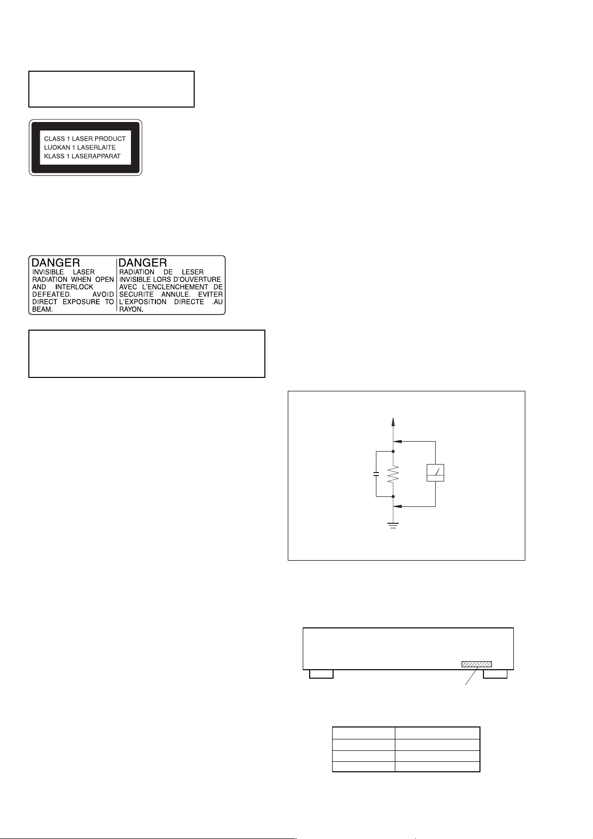
Unleaded solder
Boards requiring use of unleaded solder are printed with the lead-
free mark (LF) indicating the solder contains no lead.
(Caution: Some printed circuit boards may not come printed with
the lead free mark due to their particular size.)
: LEAD FREE MARK
Unleaded solder has the following characteristics.
•Unleaded solder melts at a temperature about 40°C higher than
ordinary solder.
Ordinary soldering irons can be used but the iron tip has to be
applied to the solder joint for a slightly longer time.
Soldering irons using a temperature regulator should be set to
about 350°C.
Caution: The printed pattern (copper foil) may peel away if the
heated tip is applied for too long, so be careful!
•Strong viscosity
Unleaded solder is more viscous (sticky, less prone to flow) than
ordinary solder so use caution not to let solder bridges occur such
as on IC pins, etc.
•Usable with ordinary solder
It is best to use only unleaded solder but unleaded solder may
also be added to ordinary solder.