SERVICE MANUAL
Sony Corporation
Home Audio Company
Published by Sony Engineering Corporation
AEP Model
UK Model
E Model
COMPACT DISC DECK RECEIVER
9-877-819-01
2004F1678-1
© 2004.06
Ver 1.0 2004.06
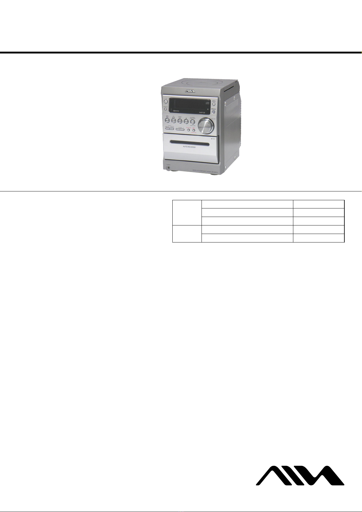
SPECIFICATIONS
CX-LEM550
Model Name Using Similar Mechanism HCD-NE5
CD Base Unit Name BU-K7BD81B
Section Optical Pick-up Name KSM-213EDP/C2NP
Tape deck Model Name Using Similar Mechanism HCD-GP5
Section Tape Transport Mechanism Type CMAL1Z240A
CX-LEM550 is the Amplifier, CD player,
TapeDeckandTunersectionin XR-EM550.
— Continued on next page —
Main unit
Amplifier section
European model:
DIN power output (rated): 20 + 20 W
(6 ohms at 1 kHz, DIN)
Continuous RMS power output (reference):
25 + 25 W
(6 ohms at 1 kHz, 10%
THD)
Music power output (reference):
38 + 38 W
Other models:
The following measured at AC 230 V or AC 120 V, 50/
60 Hz
DIN power output (rated): 20 + 20 W
(6 ohms at 1 kHz, DIN)
Continuous RMS power output (reference):
25 + 25 W
(6 ohms at 1 kHz, 10%
THD)
Inputs
MD (phono jacks): Sensitivity 450 mV,
impedance 47 kilohms
Outputs
PHONES: Accepts headphones with
an impedance of 8 ohms or
more
SPEAKER: Accepts impedance of 6 to
16 ohms.
CD player section
Laser Semiconductor laser
(λ=780 nm)
Emission duration:
continuous
Frequency response 20 Hz – 20 kHz
Tape deck section
Recording system 4-track 2-channel, stereo
Frequency response 50 – 13,000 Hz (±3 dB),
using Sony TYPE I
cassettes
Tuner section
FM stereo, FM/AM superheterodyne tuner
FM tuner section
Tuning range 87.5 – 108.0 MHz
Antenna FM lead antenna
Antenna terminals 75 ohms unbalanced
Intermediate frequency 10.7 MHz
AM tuner section
European model: 531 – 1,602 kHz
(with the tuning interval
set at 9 kHz)
Other models: 530 – 1,710 kHz
(with the tuning interval
set at 10 kHz)
531 – 1,602 kHz
(with the tuning interval
set at 9 kHz)
Antenna AM loop antenna, external
antenna terminal
Intermediate frequency 450 kHz
General
Power requirements
European model: 230 V AC, 50/60 Hz
Korean model: 220 V AC, 60 Hz
Taiwanese model: 120 V AC, 50/60 Hz
Other models: 110–120 Vor220 – 240V
AC, 50/60 Hz
Adjustable with voltage
selector
Power consumption 67 W
0.3 W (in Power Saving
Mode)