Sony CXD2701Q Product guide

IB
2
®
Semiconductor IC


Semiconductor Integrated Circuit Data Book
1992
List of Model Names/
Index by Usage
Description
Digital Filter 1C
A/D, D/A Converter
ADSP
(Audio Digital
Signal Processor)
Digital Audio
Interface IC


Semiconductor Integrated Circuit Data Book
1992
SONY,


PREFACE
This is the 1992 version of the Sony semiconductor IC data book. This book covers all the
semiconductor products manufactured and marketed by Sony.
In preparation of this data book, as much characteristic and application data as possible have
been collected and added with aview of making this book aconvenient reference for users of
Sony products. If, however, you are dissatisfied with this book in any way, please write; we
welcome suggestions and comments.
Sony reserves the right to change products and specifications without prior notice.
Application circuits shown are typical examples illustrating the operation of the devices.
Sony cannot assume responsibility for any problems arising out of the use of these circuits or
for any infringement of third party patent and other right due to same.
Unauthorized reproduction of the contents, even partial, is prohibited.
-3-

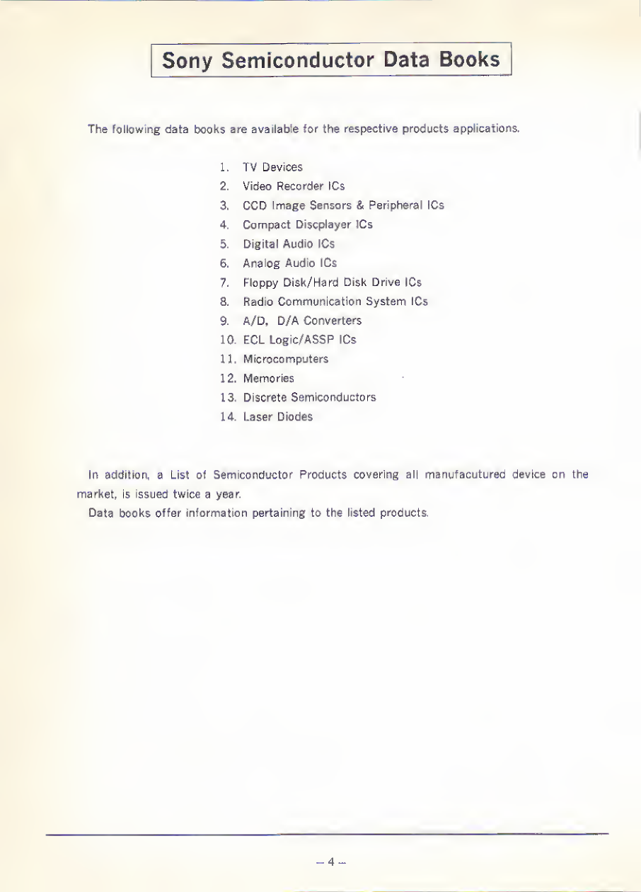
Sony Semiconductor Data Books
The following data books are available for the respective products applications.
1. TV Devices
2. Video Recorder ICs
3. CCD Image Sensors &Peripheral ICs
4. Compact Discplayer ICs
5. Digital Audio ICs
6. Analog Audio ICs
7. Floppy Dish/Hard Disk Drive ICs
8. Radio Communication System ICs
9. A/D, D/A Converters
10. ECL Logic/ASSPICs
11. Microcomputers
12. Memories
13. Discrete Semiconductors
14. Laser Diodes
In addition, aList of Semiconductor Products covering all manufactured device on the
market, is issued twice ayear.
Data books offer information pertaining to the listed products.
-4-

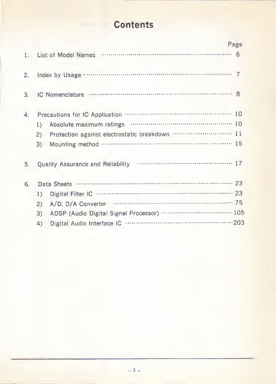
Contents
Page
1. List of Model Names —*•6
2. Index by Usage *• 7
3. IC Nomenclature *8
4. Precautions for IC Application 10
1) Absolute maximum ratings 10
2) Protection against electrostatic breakdown 11
3) Mounting method 15
5. Quality Assurance and Reliability 17
6. Data Sheets **23
1) Digital Filter IC 23
2) A/D, D/A Converter 75
3) ADSP (Audio Digital Signal Processor) 105
4) Digital Audio interface IC ••203

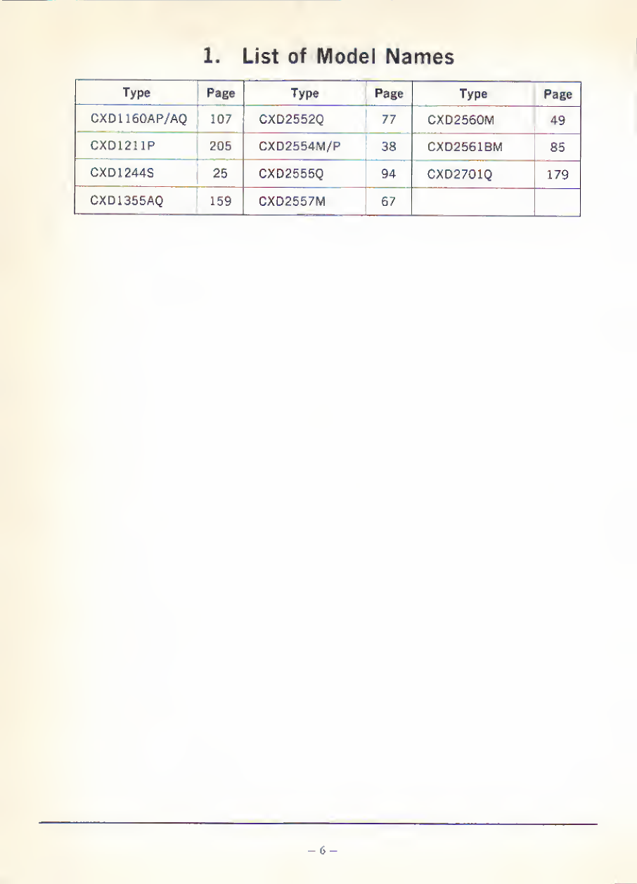
1. List of Model Names
Type Page Type Page Type Page
CXD1160AP/AQ 107 CXD2552Q 77 CXD2560M 49
CXD1211P 205 CXD2554M/P 38 CXD2561BM 85
CXD1244S 25 CXD2555Q 94 CXD2701Q 179
CXD1355AQ 159 CXD2557M 67
-6-

2. Index by Usage
1) Digital Filter IC
Type Functions Page
CXD1244S For middle class and sophisticated versions, 4/Sfs,
Filter length 213, 16/18-bit output. Attenuate deemphasis 25
CXD2554M
CXD2554P For popular version, 4/8fs, Filter length 57,
16/18-bit output. Attenuate deemphasis 38
CXD2560M 8fs, Filter length 213, 18/20-bit output. Attenuate,
deemphasis 49
CXD2557M Audio data zero detection 67
2) A/D, D/A Converter
Type Functions Page
CXD2552Q 1-bit D/A converter 77
CXD2561BM 1-bit D/A converter, 3rd order noise shaper 85
CXD2555Q 1-bit A/D-D/A converter, Built-in digital filter,
2nd order noise shaper 94
I
3) ADSP (Audio Digital Signal Processor)
Type Fu notions Page
CXD1160AP
CXD1160A0 Software realized various digital audio data.
Double accuracv arithmetic possible 107
CXD1355AQ Programmable DSP and 8is over sampling digital filter
for surround 159
Programmable DSP—Equalizer for surround
CXD2701Q Characteristics realized by fixing algorithm at equalizer
and Riving coefficient from exterior 179
4) Digital Audio Interface IC
Type Functions Page
CXD1211P Digital audio data modulation, Transmission 205
-7-

3. IC Nomenclature
1) Nomenclature of IC product name
Currently, both the conventional and new nomenclature systems are mixed in naming IC
products.
(1) Conventional nomenclature system
[Example] CX 2,0 Oil A
'—Improvement mark
"A" is affixed when specifications are partially
improved.
Product number
Identities individual product
Category number
indicates the product category in one or two digits.
3:dd3- IC: 0. I. 8:0. 20. 22
MOS IC: 5. 7, 23, 79
—Sony IC mark
(2) New nomenclature
[Example] CXA11AP
Package mark
P: Plastic Dual In-line Package
D: Ceramic Dual Inline Package
M: Small Outline LLeaded Package
L: Single In-line Package
Q: Quad Flat L-Leaded Package
S: Shrink Dual In-line Package
N: Very Small Outline Package (SSOP)
R: Very Small Quad Flat Package
Improvement mark
"A" is affixed when specifications are improved.
Product number
Identifies the individual product.
Product category mark
A;Bipolar IC
B: Bipolar digital IC
D: MOS logic IC
K: Memory, Mask ROM
P, Q: Microcomputer, Microprocessor
L: CCD signal processor
Sony IC mark
~8-

(3) Memory nomenclature
[Example] CX K5.4 64AP-OOPO
—Standby current
Access time
Package mark
P:Dual in-line package
D:Ceramic Dual In-line Package
SP :Skinny type dual inline package
M:Small outline package
J:Small outline J-leaded package
Quad Fiat J-Leaded package
TM :Thin smalt outline package (Normal)
YM :Thin small outline package (Reverse)
(Mirror image pin out)
—Improvement mark
Improvement mark is affixed when specifications
are partially improved.
—Product number
Identifies the individual product.
Product category mark
K: Memory
—Sony IC mark
I
(4) Microcomputer nomenclature
[Example] CX P506 8-QQOP
Package mark (P, Q, S)
OEM code
Product number
Indentifies the individual product.
Product category mark
P:Microcomputer
Sony IC mark
(5) Hybrid IC nomenclature
[Example] SBX 0000-00
~~PL. -Classification
Product's number Identifies individual product,
Sony hybrid IC mark
-9-

4, Precautions for IC Application
1} Absolute maximum ratings
The maximum ratings for semiconductor
devices are normally specified by "absolute
maximum ratings". The values shown in the
maximum ratings table must never be ex-
ceeded even for amoment.
If the maximum rating is ever exceeded,
device deterioration or damage will occur
immediately. Then, even if the affected
device can operate, the life will be consider-
ably shortened.
IC maximum ratings
The following maximum ratings are used
for ICs.
(1) Maximum power supply voltage Vcc
(Vdd)
The maximum voltage that can be applied
between the power supply pin and ground pin.
This power supply voltage rating is directly
related to the dielectric voltage of transistors
in the internal circuit The transistors may be
destroyed if this voltage is exceeded.
(2) Allowable power dissipation Pd
The maximum power consumption allowed
in IC.
Usage beyond the Allowable power dissipa-
tion will cause ultimate destruction through
the ICs heat generation.
(3) Operating ambient temperature Topr
The temperature range within which IC can
operate satisfactorily.
Even if this temperature range is exceeded
and some deterioration in operating charac-
teristics is noted, the IC is not always
damaged.
For some ICs, the electrical characteristics
at Ta =25'C are not guaranteed even in this
temperature range.
(4) Storage temperature Tstg
The temperature range for storing the IC
which is not operating.
This temperature is restricted by the pack-
age material, and the intrinsic properties of
the semiconductor.
(5) Other values
The input voltage Vin, output voltage Voat.
input current lin, output current lout and
other values may be specified in some ICs,
Ageneral example on the relation with
Absolute Maxium Ratings.
No assurance
Ta curve
Tstg
Ambient temperature ('Q
Main points on Circuit design.
In the circuit design the absolute maximum
ratings must not be exceeded, and it must be
designed only after considering the worst
situations among the following:
•Fluctuation in source voltage
•Scattering in the electrical characteris-
tics of electrical parts (transistors, resis-
tors, capacitors, etc.)
•Power dissipation in circuit adjustment
•Ambient temperature
•Fluctuation in input signal
•Abnormal pulses
If this allowable power dissipation is ex-
ceeded, electrical and thermal damage may
result.
This value varies with amount of IC inte-
gration in package types.
-10

2) Protection against
electrostatic breakdown
There have been problems concerning
electrostatic destruction of electronic devices
since the 2nd World War. Those are closely
related to the advancement made in the field
of semiconductor devices; this is, with the
development of semiconductor technology,
new problems in electrostatic destruction
have arisen. This situation, perhaps, can be
understood by recalling the case of MOS FET.
Electrostatic destruction is again drawing
people's attention as we are entering the era
of LSI, VLSI, and ULSI. Here are our sugges-
tions for preventing such destruction in the
device fabrication process.
Factors causing electrostatic
generation in manufacture process
Anumber of dielectric materials are used in
manufacture process. Friction of these mate-
rials with the substrate can generate static
electricity which may destroy the semicon-
ductor device.
Factors that can cause electrostatic des-
truction in the manufacture process are
shown below:
Causes of electrostatic destruction of
semiconductor parts in manufacture
process
Input
1
Item
semi-
conductor
resistor
capacitor
Parts
mounting
•belt conveyer
•work table
•human body
•Parts hox
solder dipping •dipping machine
-
visual correction
•work table
•human body
•soldering iron
J
lead cutting •cutting machine
1
sand blasting •sand blasting
machine
1
soldering correction
1•belt conveyer
rear side mounting
of parts
frame assembly
•work table
•human body
•parts box
.*soldering iron
inspection and repair
Output
-11 -

Handling precautions for the prevention of
electrostatic destruction
Explained below are procedures that must
be taken in fabrication to prevent the
electrostatic destruction of semiconductor
devices.
The following basic rules must be obeyed.
©Equalize potentials of terminals when tran-
sporting or storing.
©Equalize the potentials of the electric
device, work bench, and operator's body
that may come in contact with the semi-
conductor device,
©Prepare an environment that does not
generate static electricity.
One method is keeping relative humidity in
the work room to about 50%.
Operator
(1) Clothes
Do not use nylon, rubber and other mate-
rials which easily generate static electricity.
For clothes, use cotton, or antistatic-treated
materials. Wear gloves during operation.
protective clothing for static electricity
grounding mat
-ground strap
cotton gloves
Conductive gown
\\X\X^
(2) Grounding of operator's body
The operator should connect the specified
wrist strap to his arm.
example of grounding band
,cotton glove
snap -
,,-groundirig wire
When using acopper wire for grounding,
connect aIMn resistance in series near the
hand for safety.
(3) Handling of semiconductor device
Do not touch the lead. Touch the body of
the semiconductor device when holding.
Limit the number of handling times to a
minimum. Do not take the device out of the
magazine or package box unless it is abso-
lutely necessary.
holding of semiconductor device
DIP :yp^ can type
Equipment and tools
(1) Grounding of equipment and tools
Ground the equipments and tools that are
to be used. Check insulation beforehand to
prevent leakage.
[Check point]
•measuring instrument
•conveyer
•electric deburr brush
•carrier
•solder dipping tank
•lead cutter
•shelves and racks
-12-

grounding of carrier
conductive sheet
(2) Grounding of work table
Ground the work table as illustrated. Do
not put anything which can easily generate
static electricity, such as foam styrol, on the
work table.
grounding of work table
conductive sheet
grounding wire
Transporting, storing and packaging
methods
(1) Magazine
Use conductive, or antistatic-treated plas-
tic IC magazines,
magazine
conductive magazine
(2) Bag
Use aconductive bag to store ICs.
bag
I
conductive bag
(3) Semiconductor device case
Use aconductive case,
(4) Insertion of semiconductor device
Insert the semiconductor device during the
mounting process or on the belt conveyer.
The insertion should be done on aconductive
sheet.
(5) Other points of caution
Take note of the kind of brush material
used for removing lead chips. Use metal or
antistatic-treated plastic brushes.
13-

(3) Handling of delivery box
The delivery box used for carrying sub-
strates must be made of conductive plastic.
Do not use avinyl chloride or acrylic delivery
box, otherwise static electricity will be gener-
ated.
handling of delivery box
conductive plastic
Soldering operation
(1) Soldering iron
Use asoldering iron with a grounding wire
and an insulation resistance greater than
10MQ (DC 500V) after five minutes from
energizing.
example of solder iron tip grounding
voltage adjuster
output voltage
6to 24V 4
77T 77T
grounding plate
(4) Treatment after vehicle transport
After truck transport, place the magazine,
package box or delivery box on the grounded
rack, work table for discharging.
(5) Handling of mounted substrates
Wear cotton gloves when handling. As far
as possible, avoid touching soldered faces.
When handling mounted substrates individu-
ally, be sure to use aconductive bag. Do not
use apolyethylene bag.
handling of mounted substrate
^cotton glove
conductive bag
(2) Operation
After inserting the semiconductor device
into the substrate, solder it as quickly as
possible. Do not carry the substrate with the
inserted semiconductor device by car.
(3) Correction
When correcting parts (semiconductor
device and CR parts) after solder-dipping, be
sure to wear cotton gloves.
(4) Manual soldering
Solder with wrist strap connected to the
hand.
(5) Removing semiconductor device
Do not use the Solder-Pult when removing
the semiconductor device. Use aSolder-wick
or equivalent.
solder remover
soider-wick so.er pult
-14-

3) Mounting method
Soldering and severability
(1) Severability by JIS
JIS specifies solderability of an IC terminal
(lead) in "JIS-C7022 Test Procedure A-2".
An abstract of this standard folfows;
Rosin flux must be used, and the terminal
must be dipped in it for 5-10 seconds.
•H63A or equivalent solder must be used,
and the terminal must be dipped in the
solder which been heated to 230 iC±5:C
for 5±1 seconds,
•Using amicroscope, measure the area
{%) deposited with solder. JIS specifies
that more than 95% of the total area
should be coated with solder.
(2) Area for soldering warranty
Soldering is warranted for aspecific por-
tion of the terminal. The warranted portion is
shown in the following figure.
The tie-bar cut portion also serves as a
dam to prevent the sealing resin flowing out
during device fabrication; it is cut off at the
end of the process. Since the terminal is
exposed at the cut-off end, the area for sol-
dering is restricted. The portion near the
resin is often covered with burrs when sealing
with resin ;it is not in the soldering warranty
area.
I
warranty area for soldering
device main body
tie-bar cut portion
/
nw
Resistance to soldering heat
(1) Specification of JIS
JIS specifies the method for testing the
resistance to soldering heat. This method is
used for guaranteeing the IC resistance
against thermal stresses by soldering. An
abstract of this standard is as follows:
•Dip the device terminal only once for
10±1 seconds in asolder bath of
260'C±5*C, or for 3±g-5seconds in a
solder bath of 350 C±10'C, for adis-
tance of up to 1to 1.5 mm from the
main body.
For the solder flow system temperature
should be 260'C±5'C. To solder by
soldering iron temperature should be
350*C±10"C.
•Leave the device for more than two
hours after dipping, then measure the
device characteristics.
•Normally, the warranty is limited to 10
seconds at 260'C±5'C. The distance
between the device main body and solder
bath is 1.6 mm.
-15-

(2) Resistance to soldering heat when
mounting infrared reflow.
When surface mount devices (SOP, QFP
etc) are dipped directly into asolder pot,
the device moisture resistance may deteri-
orate and thermal stress generate cracks in
the pallet.
Carefully observe the mounting conditions,
Recommended temperature profile when
mounting infrared reflows is shown in the
figure below.
120*C ^,
235'CnTa* 10 see.
3to 4-C/set /\
50 to 300set
'
preheated part reflow part -» time
-16
Table of contents