Takenaka System TL-8000CL User manual

1/ 21
(ver.0.4)
Model: TL-8000CL
TAKENAKA SENSOR GROUP
TAKENAKA SYSTEM CO.,LTD.
□
H e a d O f f i c e
86-66 Nomizo-cho Otsuka Yamashina-ku 607-8135 Kyoto APAN
TEL:+81-75-593-9300 FAX +81-75-593-9790
□
C a m e r a D e p t . 4F Matsumasa Bld.1-17-14 Ogaya Otsu Shiga 520-2144 APAN
TEL:+81-77-545-4331 FAX +81-77-545-4335
□
Inspection S ystem Dept.
86-66 Nomizo-cho Otsuka Yamashina-ku 607-8135 Kyoto APAN
TEL:+81-75-593-9300 FAX +81-75-593-9790
□
T o k y o
O f f i c
e
2F MK Bldg. 2-2-19 Sotokanda Chiyoda-ku 101-0021 Tokyo JAPAN
TEL :+81
-
3
-
3255
-
0361
FAX:+81
-
3
-
3255
-
0362
TAKENAKA SYSTEM CO.,LTD. URL http://www.takex-system.co.jp/
TAKENAKA SENSOR GROUP
URL
http://www.ta
kex.co.jp/
Line scan camera
Instruction Manual

2/ 21
Table of Contents
1. Outline ……………………………………………… 3
2. Features ............................................................... 3
3. Internal Configuration ............................................................... 3
4. Specifications ............................................................... 4
5. Camera Interface ............................................................... 5
5-1. Signal I/O
5-2.
Pow r Conn ctor Pin-out Assignm nt
5-3.
Cam ra Link Conn ctor Pin-out Assignm nt
5-4. Bit ssignment
6. External Device Layout ............................................................... 6
7. Initial setting ............................................................... 7
7-1 Operational setting of the camera ............................................................... 7
7-1-1 SYNC setting
7-1-2 EXP mode setting
7-2 FFC Function s tting
.............................................................. 8
7-3 Gain control
.................................................................... 9
7-3-1 ADC gain s tting
7-3-2 Analog gain s tting
8. Notes ............................................................... 10
Suppl m ntal data
I. Exposure Control ................................................................................... 11
II. Timing Chart ......................................................................................... 12
III. Communication Protocol ....................................................................... 13
IV. Setup Steps of Hyper Terminal............................................................. 15
V. Communication setting ......................................................................... 19
VI. External Dimensions ............................................................................. 21

3/ 21
●
Block diagram
1. Outline
Th TL-8000CL is a High-R solution Digital Lin Scan Cam ra adopting 8,192-Pix l CMOS Imag S nsor.
2. Features
●
Capabl of p rforming high-r solution insp ction with 8,192 pix ls imag s nsor.
●
Th 7µm×7µm pix l siz s nsor nabl s high-d finition imag acquisition.
●
Th high sp d op ration at 320MHz data rat .
●
Th Cam raLink int rfac (M dium Configuration at 10bit output) allows asy conn ction with a
fram grabb r board.
●
GAIN and OFFSET charact ristic can b asily adjust d with s rial communication (Cam raLink sp c.).
●
Equipp d with Global shutt r function and FFC function.
●
Equipp d with Anti-blooming function.
●
Singl DC12V pow r sourc and Low pow r consumption ar r aliz d.
●
Possibl to g t stabl vid o signal d spit a chang of ambi nt t mp ratur , as th dark curr nt
corr ction circuit is incorporat d.
●
R duction in siz and w ight has b n r aliz d by adopting uniqu circuit and m chanism d sign.
3. Internal Configuration
High-s nsitiv and high-sp d CMOS s nsor with 8,192 ff ctiv pix ls, of which pix l siz is 7μm
squar , is quipp d.
Charg s accumulat d in singl -row photo diod s ar output through two shift r gist rs, r sp ctiv ly.
(On for ODD numb r d charg s, and th anoth r for EVEN numb r d charg s)
Block diagram of CMOS d vic and Sp ctral s nsitivity charact ristic ar d scrib d b low.
D1
D3
D2
D0
D2049
D4097
D2048
Bas e
Por t A Base
Port B B ase
P ort C Mi deum
Po rt D
F PGA 1
CPU
TXD
RXD
CC1
C a me r a Li n k
B a se Co nf i gur at i on
CDS _AD Regi ste r CDS_ AD R egis ter CDS_ AD R egis ter CDS _AD Regi ster
P hoto Dio de
D2050
D2047
D2046
D2051
D4096
D4095
D4094
D4098
D6144
D6143
D6142
D6145
D6146
D6147
D8192
D8191
D8190

4/ 21
●
Sp ctral
R spons
4. Specifications
Number of pixels 8192 pixels
Pixel size
7
μ
m×7
μ
m
Photo array length 57.3 mm
Data rate 320 MHz (80MHz× TAP)
Scan rate (scan/sec) 35 kHz
Line transfer pulse input
2
8.57
μ
sec (Min.)
Video output (Digital output) 8/10 bit Medium Configuration
Sensitivity
(DNnj/cm
2
)
gain1=1.2, gain2= .8
Saturated exposure amount (ke-) 6 (typical value)
Output ununiformity 10% standard
at 50% of saturation output(on the element)
Dynamic range 60 dB (on the element)
Flange focus 19.55 mm
Power supply +12V ±0.5V (0.5A or less)
Operational ambient temperature 0 to + 0℃
Operational humidity range 85% MAX
Storage temperature range -10℃ to +65℃
Weight 720g or less
External dimension (mm)
100(W)×1
00(H)×3
(D) Excluding protruding portion
Lens mount M72, P=0.75mm
%
60.00
55.00
50.00
45.00
40.00
35.00
30.00
25.00
20.00
15.00
350 400 450 500 550 600 650 700 750 800 850 900
Wavelength [nm]
Wavelength [nm]Wavelength [nm]
Wavelength [nm]
e-/ph[%]

5/ 21
Pin No. Signal name Pin No. Signalname
1 Shield 14 Shield
2 X0- 15 X0+
3 X1- 16 X1+
4 X2- 17 X2+
5 Xclk- 18 Xclk+
6 X3- 19 X3+
7 Ser TC+ 20 Ser TC-
8 Ser TFG- 21 Ser TFG+
9 CC1- 22 CC1+
10 CC2+ 23 CC2-
11 CC3- 24 CC3+
12 CC4+ 25 CC4-
13 Shield 26 Shield
Base Configuration Connector
Camera Control Configration
Signal name Connection
CC1 EX. SYNC
CC2 Spare
CC3 Spare
CC4 Spare
Pin No. Signalname Pin No. Signal name
1
Shield
14
Shield
2
Y0-
15
Y0+
3
Y1-
16
Y1+
4
Y2-
17
Y2+
5
Yclk-
18
Yclk+
6
Y3-
19
Y3+
7
100Ω
20
terminated
8
Z0-
21
Z0+
9
Z1-
22
Z1+
10
Z2-
23
Z2+
11
Z clk-
24
Z clk+
12
Z3-
25
Z3+
13
Shield
26
Shield
Medium and Full Configuration Connector
5. Camera Interface
5-1 Signal I/O
Th lin s nsor is conn ct d to th Fram grabb r board via two Cam ra Link cabl s.
5-2 Pow r Conn ctor Pin-out Assignm nt
5-3 Cam ra Link Conn ctor Pin-out Assignm nt
1
26 14
13
Camera Link connector pin-out
Pin No.
Signal name
Pin No.
Signal name
1
+12V
4
GND
2
+12V
5
GND
3
+12V
6
GND
1
2
34
5
6
Power connector (HR10 -7P-6S HIROSE)
(Pin-out viewed from outside the camera)
Power connector (DC12V)
Power indicator
Bas e Medium
Power
Camera Lin
k connector
Pixel #1
Pixel #8192

6
/
21
5-4 Bit Assignm nt
Port
Port A 1
~
2047
ODD
Port B 2048
~
4095
EVEN
Port C 4096
~
6143
ODD
Port D 6144
~
8192
EVEN
6. E ternal Device Layout
CameraLink
Captureboard
Po wer suppl y
(
AD-50)
CaneraLinkcable
※
※
CameraLink cable
14B26-SZLB-
*
00-0LC
(
Medium/FullCofig. Standard type)
Powercable
(
6PS-
××
)
*
represents cablelength(m)
Port/bit 8-bit 10-bit Port/bit 8-bit 10-bit
Port A0 A0 A0 Port B4 B4 B8
Port A1 A1 A1 Port B5 B5 B9
Port A2 A2 A2 Port B6 B6 nc
Port A3 A3 A3 Port B7 B7 nc
Port A4 A4 A4 Port C0 C0 B0
Port A5 A5 A5 Port C1 C1 B1
Port A6 A6 A6 Port C2 C2 B2
Port A7 A7 A7 Port C3 C3 B3
Port B0 B0 A8 Port C4 C4 B4
Port B1 B1 A9 Port C5 C5 B5
Port B2 B2 nc Port C6 C6 B6
Port B3 B3 nc Port C7 C7 B7
Base
connector
Port/bit 8-bit 10-bit Port/bit 8-bit 10-bit
Port D0 D0 D0 Port F4 nc D8
Port D1 D1 D1 Port F5 nc D9
Port D2 D2 D2 Port F6 nc nc
Port D3 D3 D3 Port F7 nc nc
Port D4 D4 D4 Port G0 nc nc
Port D5 D5 D5 Port G1 nc nc
Port D6 D6 D6 Port G2 nc nc
Port D7 D7 D7 Port G3 nc nc
Port E0 nc C0 Port G4 nc nc
Port E1 nc C1 Port G5 nc nc
Port E2 nc C2 Port G6 nc nc
Port E3 nc C3 Port G7 nc nc
Port E4 nc C4 Port H0 nc nc
Port E5 nc C5 Port H1 nc nc
Port E6 nc C6 Port H2 nc nc
Port E7 nc C7 Port H3 nc nc
Port F0 nc C8 Port H4 nc nc
Port F1 nc C9 Port H5 nc nc
Port F2 nc nc Port H6 nc nc
Port F3 nc nc Port H7 nc nc
Medium and Full connector

7
/
21
7. Initial setting
lways use FFC function for this camera.
(
Flat fi ld corr ction is a function us d to improv non-uniform imag arising from imp rf ctions
contribut d by l ns, pictur l m nt tc.
)
The following settings are all made by communication command of Hyper terminal (See P.15-18).
Make the setting according to TL-8000C_RS232C communication protocol (P.12 -13 )
(Refer to
S rial Communication Protocol P.10 -13
)
t Hyper terminal
cfg The following list is obtained.
7-1 Operational setting of the camera
7-1-1 SYNC setting
Sync=N Sets the camera SYNC.
1: External synchronization (Ext Sync)
2: Internal synchronization (Int Sync)
7-1-2 EXP mode setting
expc= N Sets the Exposure control states.
0: Line period exposure
1: Fixed time exposure (value of expt)
2: Pulse width exposure
(Refer to P.14 Exposure control for the detail)
expt= N Sets the Exposure time(Fixed value) of the camera.
N:0-255 Unit 6.35µsec

8
/
21
7-2 FFC Function s tting
Flat fi ld corr ction (also call d Shading corr ction) is a function us d to improv non-uniform imag
arising from imp rf ctions contribut d by l ns, pictur l m nt tc. (B sur to us FFC function wh n
using this cam ra.)
・S t th shading l v l to th high st valu of vid o signal.
<S tup st ps>
1. Dark l v l corr ction
shad = 0 Turns off shading function
“R s ts” th shading gain valu r maining in th cam ra.
shad = 4 Enabl s shading data ntry.
shd-go = 1 S l cts th shading gain s tting.
shd-dat= 0 Inputs “0” as shading gain valu .
shd_s t S ts th shading data.
shd_to = N S ts th targ t gray l v l of Dark l v l.
Initial valu =6 N : 0 to 255
Th n put a cap ov r th l ns.
shad = 6 Starts th shading corr ction for Dark l v l.
Compl t d wh n “OK” is display d.
2. Light l v l corr ction
R mov th l ns cap and s t th targ t gray l v l of vid o l v l.
Mak th l v l adjustm nt by changing l ns ap rtur or xposur tim using plain whit targ t sampl ..
(Not : Mak th adjustm nt und r th condition that a for ign obj ct is not within th visual fi ld.)
shd_tg = N S ts th targ t gray l v l of Light l v l.
Initial valu =150 N : 0 to 255
(Wh r th Light l v l should b s t at th high r l v l than that of FFC ”OFF”(at
Dark FFC)
shad = 5 Starts th shading corr ction for Light l v l.
Compl t d wh n “OK” is display d.
shd_ psv All shading corr ction valu s ar stor d in EPROM.
Compl t d wh n “OK” is display d.
shad = 1 Turns off shading function
sav Syst m s ttings ar stor d in EPROM.
Compl t d wh n “OK” is display d.
<Suppl m ntary not >
If th cam ra gain is chang d using “again=N” or “logrl=N”, b sur to mak th Dark l v l corr ction and
Light l v l corr ction onc again.
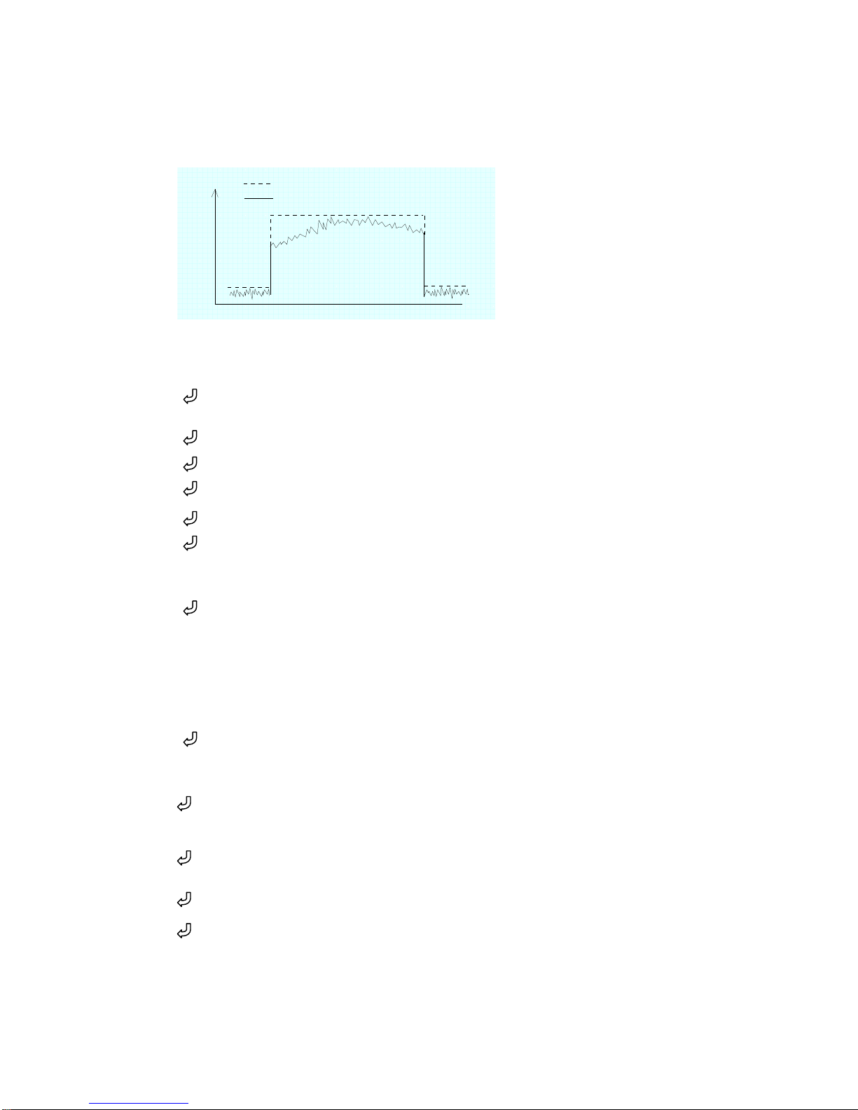
Waveform
before shading
255
0
Waveform
aftershading
◆
Dark level (shd-tg) set 8bit
◆
Light level (shd-to) set 8bit

9
/
21
7-3 Gain control
7-3-1 ADC gain s tting
Logrl=N S ts th ADC gain
Initial valu =40 N : 0 to 255
Th r lationship b tw n th s tting valu and ADC gain is shown in th
following chart.
7-3-2 Analog gain s tting
again=N S ts th Analog gain of th cam ra.
0: on -fold
1: four-fold
※ It is r comm nd d to us “7-3-1 ADC gain s tting”, as th four-fold valu of Analog gain is too
s nsitiv and is mor lik ly to wors n th standard d viation.
※ It is r comm nd d to mak Flat fi ld corr ction again aft r gain changing.
※ Do not us th gain command “gain position” which has b n us d in th conv ntional product.
V rtical axis:
Scal factor
(1 at logrl=40)
Horizontal axis: S tting valu N

10
/
21
8. Notes
■
If dust sticks to th prot ctiv glass of CMOS imag s nsor, imag signal cannot b output from th
photo diod s on this part and it xhibits symptoms similar to d f ct pix ls.
In this cas , blow away dusts with an air spray. How v r, not that wat r dropl t may b spray d out
from an air spray.
■
Do not stor th quipm nt at th plac wh r is subj ct to dir ct sunlight.
■
Do not r mov a cov r and do not ins rt/r mov a Cam ra Link conn ctor wh n applying curr nt to
th quipm nt. It caus s th quipm nt to malfunction.
■
Wh n disposing of th quipm nt, d l gat th task to th industrial wast disposal contractor.
And x cut th disposing proc dur following r lat d laws and r gulations.
■ Do not us th quipm nt in an nvironm nt subj ct to int ns l ctromagn tic or l ctrostatic fi ld.
Also, if th arth conn ction is imp rf ct, th imag signal may contains inductiv nois compon nts
and it caus s th quipm nt to malfunction.
Th sp cifications and op rational d tails d scrib d in th manual ar subj ct to chang for p rformanc
improv m nt or oth r r asons without notic .

11
/
21
F
FF
Fi
ii
ix
xx
xe
ee
ed
dd
d t
tt
ti
ii
im
mm
me
ee
e e
ee
ex
xx
xp
pp
po
oo
os
ss
su
uu
ur
rr
re
ee
e(expc=1,expt=A,explt=B)
Exposure during the period of the equation below
fr o m th e t i mi n g of le a di ng ed g e of EX T .S Y NC (C C 1) .
Exposure time (A×256+B-44)×0.025 (μsec)
Mi ni m um ex po s ur e t im e 5 . 3 μ se c
* N ot e t h at th e m in i mu m p er i od of E X T. S YN C i s 2 8. 57 μ s e c i n th e F i xe d t im e e x po su r e m od e .
S T- 1 D AT A o u tp ut
period
ST - 2 D AT A o ut p ut pe ri o d
P IX E L PO R T A ~ D
2 04 8x 8
S T -1 D A TA ou t pu t p er i od
*1 2280CLOCK
S T OU T -1
EX T .S YN C I N
(C C 1)
Line Valid
S T- 1
Exposur e t ime
ST - 2
Exposu re ti me
S T O UT -2
*1
2.5μsec
P
PP
Pu
uu
ul
ll
ls
ss
se
ee
e w
ww
wi
ii
id
dd
dt
tt
th
hh
h e
ee
ex
xx
xp
pp
po
oo
os
ss
su
uu
ur
rr
re
ee
e(expc=2)
Ex po s ur e d ur i ng th e p er i od of t h e p ul se wi d th of E X T. S YN C( C C1 ) .
M im i mu m e x po su r e t im e 5 μ s ec
* N ot e t ha t t h e mi n im u m pe r io d o f E XT . SY N C is 28 . 67 μ s ec in th e P ul s e w id th ex p os ur e m o de .
E X T. SY N C I N
(CC1)
Line Valid
ST-1
Exp osu re t ime
S T- 1 D AT A o u tp ut pe r io d
ST-2
Exp osur e t ime
ST - 2 D AT A o ut p ut pe ri o d
P I XE L P OR T A ~ D
2 0 48 x8
*1
Exposu re t ime
2 .5 μ s ec 2. 5 μ se c
S T -0 DA TA ou t pu t p er i od
*1 2280CL OCK
L
LL
Li
ii
in
nn
ne
ee
e p
pp
pe
ee
er
rr
ri
ii
io
oo
od
dd
d e
ee
ex
xx
xp
pp
po
oo
os
ss
su
uu
ur
rr
re
ee
e(expc=0)
Exposure during each period of EXT.SYNC(CC1)
Exposure time=Cycle timeー2.5μsec * * : a t 32 0 MH z
D
a ta R a te
P I XE L P OR T A ~ D
20 4 8 × 4
Exposu re ti me
E XT . SY NC IN
(CC1)
ST-2
L i ne Va l id
ST-1 ST-3
ST - 1 DA T A
S T- 0 D AT A S T- 2 D AT A
Ex posu re ti me Exp osu re ti me
Exposu re t ime
*1 2280 CLO CK
*1
Ⅰ
ⅠⅠ
Ⅰ.
..
.Exposure control

12
/
21
Ⅱ
ⅡⅡ
Ⅱ.
..
.Timing chart
S1
S2
S2046
S2047
S2048
P IX E L C L OC K
E X S YN C In
( CC 1 I N )
L IN E VA L I D
P IX E L D A TA
P OR T A
( OS 1 )
One Line output period (2285 CLOCK)
S2045
S2044
P IX E L D A TA
P OR T B
( OS 2 )
S2050
S2049
S4092
S4093
S4094
S4096
S4095
Effective data period
P IX E L D A TA
P OR T D
( OS 2 )
P IX E L D A TA
P OR T C
( OS 1 )
S8192
S8191
S8189
S8190
S8188
S4098
S4097
S6140
S6142
S6141
S6143
S6144
S6146
S6145
.

13
/
21
Command Name Format Argument Return value Explanation
Get ID id[?]<CR> Non ID(De ault:0) Get the camera ID
*1 This is or multiple camera management
Set ID id=N<CR> N:0~255 OK Set the camera ID
*1 This is or multiple camera management
Get Bit Setting bit[?]<CR> Non 10:10 bit setting
8:8bit setting
Get the bit setting
Set Bit bit=N<CR> N=10:10bit setti ng
N=8:8bit setting
OK Set the camera bit
Get Sync. sync[?]<CR> Non 0:Don't u se Get the Sync system o the camera
1:Ext Sync
2:Int Sync
3:Don't use
Set Sync. sync=N<CR> N=0:Don't use OK Set the Sync system o the camera
N=1:Ext Sync Ext Sync is rom CC1.
N=2:Int Sync
N=3:Don't use
Get Exposure expc[?]<CR> Non 0:Line peri od exposure Get the Exposure control status
Control 1:Fixed time exposure
2: Pulse width exposure
Set Exposure expc=N<CR> N=0:Line period exposure OK Set the Exposure control status
Control N=1:Fixe d time exposure
N=2: Pulse width exposure
Get Exposure expt[?]<CR> Non 0-255 :Exposure time Set the Exposure time
Time explt[?]<CR>
Set Exposure expt=N<CR> N=0-255:Exposure time OK Get the Exposure time
Time explt=N<CR>
Get Gain Position gainpos[?]<CR> Non 1-8:Gain position Get the Gai n position
Set Gain Position gainpos=A<CR> A=1-8:Gain position OK Set the Gain posi tion
Get chXgainA
chXgainA[?]<CR>
X=1-4:ch 0-255:Gain level
Get the Gain level o each gain postion o
A=1-8:Gain position each channel
Set
chXgainA=N<CR>
X=1-4:ch OK
Set the Gain level o each gain postion o
chXgainA A=1-8: Gain position each channel
N=0-255: Gain level
Check check<CR> Non OK Communi cation test
Save save<CR> Non OK Save settings to the EEPROM
Load load<CR> Non OK Load settings rom the EEPROM
Version ver<CR> Non Version
Get the version number o the program or
the microcomputer control
Model model<CR> Non Model Get the camera model
Revision rev<CR> Non Revision Get the version number o FPGA
Initialize init<CR> Non OK Load the actory settings
con ig c g<CR> Non (Data output) Get the all current settings
*1…ID can be saved on the user area of the EEPROM by the save command. It cannot be cleared by the clear command.
GainSystem UserSync selectionExposure control
Exposure time
Bit
Ⅲ
ⅢⅢ
Ⅲ.
..
.Communication protocol

14
/
21
Command Name Format Argument Return value Explanation
Shade Control shade=N<CR> 0:OFF O Shade control mode
Mode 1:ON Getting/setting
2:Data out (Note.4)
3:Data in
4:Data all in
5:Auto shade for gain
6:Auto shade for offset
7:ON(offset only)(Note.6)
shade[?]<CR> Non 0:OFF
1:ON
2:Data out
3:Data in
4:Data all in
5:Auto shade for gain
6:Auto shade for offset
7:ON (offset only)(Note.6)
Gain/Offset shd_go=N<CR> 0:OFF O Target value
1:Gain Getting/setting
2:Offset (Note.3)
shd_go[?]<CR> Non 0:OFF
1:Gain
2:Offset
Pixel Address shd_ad0=N<CR> N:0-255 O Correction targeted pixel
(Lower) (The lower address)
shd_ad0[?]<CR> Non 0-255 Getting/setting
(Note.2)
Pixel Address shd_ad1=N<CR> N:0-255 O Correction targeted pixel
(Upper) (The upper address)
shd_ad1[?]<CR> Non 0-255 Getting/setting
(Note.2)
Value set shd_dat=N<CR> N:0-255 O Data value setting
shd_dat[?]<CR> Non 0-255 Data value getting
Taget Level for shd_to=N<CR> N:0-255 O Correction targeted level
black level Getting/setting
shd_to[?]<CR> Non 0-255 for black level.
(Note.2)
Taget Level for shd_tg=N<CR> N:0-255 O Correction targeted level
gray level Getting/setting
shd_tg[?]<CR> Non 0-255 for gray level.
(Note.2)
Data set shd_set<CR> Non O Data set
EEPROM load shd_epld<CR> Non O EEPROM all load
EEPROM save shd_epsv<CR> Non O EEPROM all save
EEPROM clear shd_epcl<CR> Non O EEPROM all clear
Note.2: Correction targeted pixel address: [shd_ad1] x 256 + [shd_ad0]
Note.3: Gain or Offset has to be chosen before using "Data set" command.
Note.4: When setting “shade” to 2, the setting status is output as is the case in video signal from Video out port.
Note.5: Only the value of EEPROM is cleared. RAM is not cleared.
Note.6: When setting “shade” to 7,the gain doubles.
SHADE

15
/
21
[Setup of Hyper terminal ] (In the case of Microsoft Windows2000)
1)
Select “Start”→ “Programs”→” ccessories”→”Communications”→”Hyper Terminal”
2)
The windows will appear with the picture below.
3)
When the next picture appears, enter any name.(e.g. GM _RS232C)
Then click the “OK” button.
4)
When the next picture appears, select “ COM? ” on Connect using.
(? changes depending on the setting of the computer. )
Then click the “OK” button.
Ⅳ
ⅣⅣ
Ⅳ.
..
.Setup steps of Hyper Terminal

16
/
21
5)
When the next picture appears, select each items as follows.(9600,8,None,1,Non)
Then click the “OK” button.
6)
The next picture will appear.
7)
Select [File]→ [Properties]
[Network transmission setting]
Baud rate : 9600 bps
Data length : 8 bit
Start bit : 1 bit
Stop bit : 1 bit
Parity : Non
Xon / Xoff control : Non

17
/
21
8)
When the next picture appears, select “Settings” tag.
9)
When the next picture appears, click the “ SCII Setup” button.
10)
When the next picture appears, select each items as follows.(☑, ☑, 0, 0,☑, blank, blank)
Then click the “OK” button.
11)
The screen display will return to the screen of 9).
Then click the OK button.

18
/
21
12)
End of setup.
Confirm the connection of the camera ,
enter “check” on the screen below
and then send it out.
If “OK” is displayed on the screen, communication processing has been completed.
13) Select “Start”→ “Programs”→” ccessories”→”Communications”→”Hyper Terminal” →”(*1) ”, when to
launch the Hyper terminal again with the same settings after having exited the above screen.
*1………The name which was entered at section 3)

19
/
21
[Communication settings]
Baud rate :9600bps
Data Length :8bit
Start Bit :1bit
Stop Bit :1bit
Parity :Non
Xon / Xoff Control :Non
[Communication overall]
1.
Referring
To refer to the status of the camera.
e.g. Id? <CR> To refer to the camera ID.
2.
Setting
To set the status of the camera.
e.g. sync=1 <CR> To set SYNC system to EXT.SYNC
[Glossary]
[ ] ……omissible
<CR> ……carriage return
N ……arbitrary numeral indicating some value
……arbitrary numeral indicating G IN position
X ……arbitrary numeral indicating Channel
Gain position……G IN position of the camera
Channel …….Channel to specify the G IN control device for each CCD output line
EEPROM …….EEPROM incorporated in the camera
[Notes]
・Command name must be lower-case. Upper-case character is not valid.
・Input character must be one-byte character. Double-byte character is not valid.
・Blank is not valid.
・Line feed code is indicated by “CR(0x0D)”. nd also “LF(0×0 )” and “CR+LF” are usable.
However returning line feed code must be CR only.
<When using Hyper terminal>
・Retyping is required In case of inputting error.(Correction by cursor movement is not valid.)
Ⅴ
ⅤⅤ
Ⅴ.
..
.Communication setting

20
/
21
[ Description of exceptional case]
*NG is returned in case of command input error or inputting nonexistent command.
e.g. : Command input error (Gain position No. is not designated. )
ch1gain=96
NG
e.g. : Input of nonexistent command
chake
NG
*NE is returned in case of numeric entry error.
e.g. : Input error (Input value is beyond the setting range.)
gainpos=96
NE
e.g. : Input error (Input value is beyond the setting range.)
ch1gain1=2000
NE
*NC is returned in case of inputting invalid value under the condition that the ctrl setting (DIP-SW setting)
is 0.
e.g. :
ch1gain=96 (at ctrl=0)
NC
*TO is returned when a command input period overruns the time-out period (15 sec.).
e.g. :
gainpo (No CR entry)
TO
*” ? ” at the bottom of Command is omissible
e.g. :
id
0
Table of contents
Other Takenaka System Color Camera manuals