TOKYO ELETECH FM3-64SD1NQ User manual

2012/07/04 TOKYO ELETECH
FM3-64SD1NQ / FM3-120SD1NQ MANUAL
1. Power supply selection ( Note: * default setting)
POWER SOURCE
CN44
DC 5V 1-2
USB VBUS 2-3 *
JTAG V-SUPPLY Open
VCC SELECTION
CN43 CN45 CN46 CN47 CN48
3.3V 2-3 * 1-2 * 1-2 * 1-2 * 1-2 *
5V 2-3 2-3 2-3 1-2 1-2
JTAG V-supply 1-2 1-2 1-2 1-2 1-2
Note: CN46 should be OPEN when USB-less FM3 is used.
2. Switch, Jumper Pin Settings ( Note: * default setting )
FUNCTION SETTING ACTION
SW1 RESET PUSH ON RESET
PUSH OFF NOT RESET
SW2 MD0 1-2 HIGH
2-3 * LOW
SW3 MD1 1-2 HIGH
2-3 * LOW
SW7 FM3 USB SELECTION 5-6 2-3 USB HOST
4-5 * 1-2 * USB DEVICE
CN22
CN23 CAN TRANSCEIVER
MODE CONTROL CN22 1-2 *
CN23 OPEN * STANBY MODE
CN22 OPEN
CN23 1-2 HI-SPEED MODE
CN24 TX0_0 (CAN TX) 1-2 CONNECT TO CAN TRANSCEIVER
2-3 * OPEN
CN26 RX0_0(CAN RX) 1-2 CONNECT TO CAN TRANSCEIVER
2-3 * OPEN
CN27 CAN RX and TX CONNECTION 1-2 SHORT
2-3 * OPEN
CN28 SOT0_0 (UART TX) 1-2 CONNECT TO RS TRANSCEIVER
2-3 * OPEN
CN29 SIN0_0 (UART RX) 1-2 CONNECT TO RS TRANSCEIVER
2-3 * OPEN
CN31 UDP0 (USB D+) 1-2 CONNECT TO USB CONNECTOR
2-3 * GND

2012/07/04 TOKYO ELETECH
CN32 UDP1 (USB D-) 1-2 CONNECT TO USB CONNECTOR
2-3 * GND
CN33 P0B 1-2 CONNECT TO VBUS CONTROL IC FLG
2-3 * OPEN
CN34 P0C 1-2 CONNECT TO VBUS CONTROL IC EN
2-3 * OPEN
CN35 P61 1-2 CONNECT TO USB D+ PULL-UP CONTROL
2-3 * OPEN
CN36 TEST CONNECTOR 1-2 * ALWAYS SET THIS
2-3 DO NOT SET THIS
CN37 P60 (USB CONN. DET.) 1-2 CONNECT TO USB VBUS
2-3 * OPEN
CN38 TEST CONNECTOR N/A DO NOT SET THIS CONNECTOR
CN39 TEST CONNECTOR N/A DO NOT SET THIS CONNECTOR
CN40 TDO 1-2 * PULL-UP
2-3 N/A
CN41 TCK 1-2 * PULL-UP
2-3 PULL-DOWN
CN42 XTRST 1-2 * PULL-UP
2-3 N/A
JP1 TEST CONNECTOR N/A DO NOT SET THIS CONNECTOR
JP2 AVRH 1-2 * CONNECT TO AVCC

2012/07/04 TOKYO ELETECH
Revision history:
2012/06/07 Initial revision
The following precautions apply to the product described in this manual.
Before moving the product, be sure to turn off all the power supplies and unplug the cables. Watch your step when carrying the
product. Do not use the product in an unstable location such as a place exposed to strong vibration or a sloping surface.
Do not place anything on the product or expose the product to physical shocks. Do not carry the product after the power has
been turned on. Doing so may cause a malfunction due to overloading or shock.
Since the product contains many electronic components, keep it away from direct sunlight, high temperature, and high humidity
to prevent condensation. Do not use or store the product where it is exposed to much dust or a strong magnetic or electric field
for an extended period of time. Inappropriate operating or storage environments may cause a fault.
Use the product within the ranges given in the specifications. Operation over the specified ranges may cause a fault.
To prevent electrostatic breakdown, do not let your finger or other object come into contact with the metal parts of any of the
connectors. Before handling the product, touch a metal object (such as a door knob) to discharge any static electricity from your
body.
Always turn the power off before connecting or disconnecting any cables from the product. When unplugging a cable, unplug
the cable by holding the connector part without pulling on the cable itself. Pulling the cable itself or bending it may expose or
disconnect the cable core, resulting in a fault.
It is recommended that it be stored in the original packaging. Transporting the product may cause a damage or fault. Therefore,
keep the packaging materials and use them when re-shipping the product.
The contents of this document are subject to change without notice.
The information, such as descriptions of function and application circuit examples, in this document are presented solely for the
purpose of reference to show examples of operations and uses of Spansion Inc. and other vendors device; TOKYO ELETECH
and Spansion Inc. do not warrant proper operation of the device with respect to use based on such information. When you
develop equipment incorporating the device based on such information, you must assume any responsibility arising out of such
use of the information. TOKYO ELETECH and Spansion Inc. assume no liability for any damages whatsoever arising out of the
use of the information.
Any information in this document, including descriptions of function and schematic diagrams, shall not be construed as license
of the use or exercise of any intellectual property right, such as patent right or copyright, or any other right of TOKYO
ELETECH or any other right of Spansion Inc. or any third party or do TOKYO ELETECH and Spansion Inc. warrant
non-infringement of any third-party's intellectual property right or other right by using such information. TOKYO ELETECH
and Spansion Inc. assume no liability for any infringement of the intellectual property rights or other rights of third parties which
would result from the use of information contained herein.
The products described in this document are designed, developed and manufactured as contemplated for general use, including
without limitation, ordinary industrial use, general office use, personal use, and household use, but are not designed, developed
and manufactured as contemplated (1) for use accompanying fatal risks or dangers that, unless extremely high safety is secured,
could have a serious effect to the public, and could lead directly to death, personal injury, severe physical damage or other loss
(i.e., nuclear reaction control in nuclear facility, aircraft flight control, air traffic control, mass transport control, medical life
support system, missile launch control in weapon system), or (2) for use requiring extremely high reliability (i.e., submersible
repeater and artificial satellite). Note that TOKYO ELETECH and Spansion Inc. will not be liable against you and/or any third
party for any claims or damages arising in connection with above-mentioned uses of the products.
Any semiconductor devices have an inherent chance of failure. You must protect against injury, damage or loss from such
failures by incorporating safety design measures into your facility and equipment such as redundancy, fire protection, and
prevention of over-current levels and other abnormal operating conditions.
Exportation/release of any products described in this document may require necessary procedures in accordance with the
regulations of the Foreign Exchange and Foreign Trade Control Law of Japan and/or US export control laws.
The company names and brand names herein are the trademarks or registered trademarks of their respective owners.

FM3-64SD1NQ (FIGURE EXAMPLE BELOW)
FM3-120SD1NQ CN17 J AG
E SICA20C20Z-GA101
(NO MOUN ED)
DC5V CN8 E M CN9 J AG
USB VBUS POWER

5
5
4
4
3
3
2
2
1
1
D D
C C
B B
A A
MCUVCC MCUVCC USBVCC
AVCC
P62 [2]
P3F[2] P3E[2] P3D[2] P3C[2] P3B[2] P3A[2] P39[2] P33[2] P32[2] P31[2] P30[2] P52[2] P51[2] P50[2]
P61 [2,4]
P60 [2,4]
P0F [2]
P19 [2]
P18 [2]
P21 [2,3]
P22 [2,3]
P23 [2]
P0C [2,4]
P0A [2]
P0B [2,4]
X0A[2,6] X1A[2,6] INITX[2,3,5]
P04 [2,5]
P00 [2,5]
P01 [2,5]
P02 [2,5]
P03 [2,5]
MD0[2,3] X0[2,6] X1[2,6] P10 [2]
MD1[2,3]
P11 [2]
P12 [2]
P13 [2]
P14 [2]
P15 [2]
P17 [2]
P4E[2] P4D[2] P4C[2] P4B[2] P4A[2] P49[2]
UDP0 [2,4]
UDM0 [2,4]
C[2] AVRH [2]
Ed.
Desig. Date Desig. Check Appr. Description
Title
Check Appr.
Draw.No.
Fujitsu Semiconductor Limited Sheet
FM3 Evaluation Board (LQFP-64/LQFP-120)
61
LQFP-64
Ed.
Desig. Date Desig. Check Appr. Description
Title
Check Appr.
Draw.No.
Fujitsu Semiconductor Limited Sheet
FM3 Evaluation Board (LQFP-64/LQFP-120)
61
LQFP-64
Ed.
Desig. Date Desig. Check Appr. Description
Title
Check Appr.
Draw.No.
Fujitsu Semiconductor Limited Sheet
FM3 Evaluation Board (LQFP-64/LQFP-120)
61
LQFP-64
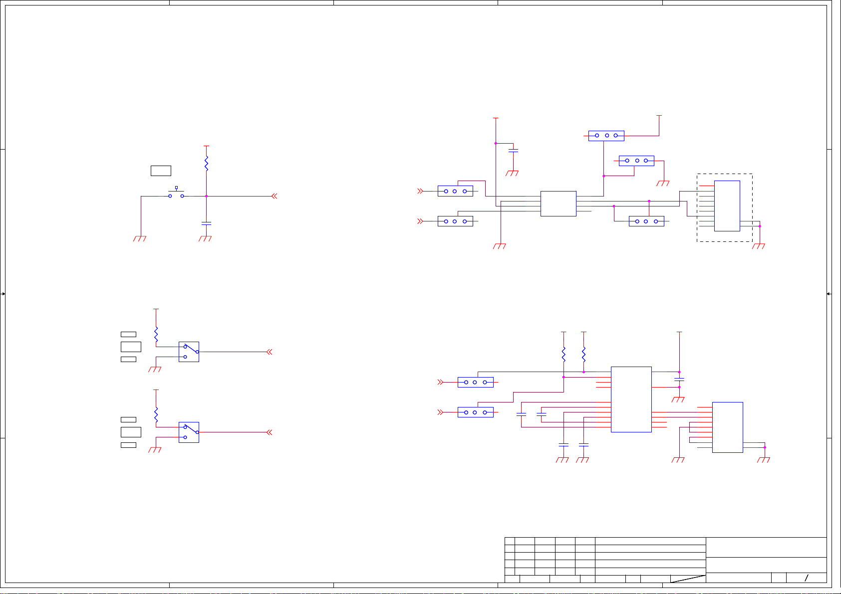
MCU_1
C4
0.1uF
C4
0.1uF
C3
0.1uF
C3
0.1uF
M1
FM3_LQFP-64
M1
FM3_LQFP-64
VCC
1P50/INT00_0/AIN0_0/SIN3_1/RTO10_0/MDATA0
2P51/INT01_0/BIN0_2/SOT3_1/RTO11_0/MDATA1
3P52/INT02_0/ZIN0_2/SCK3_1/RTO12_0/MDATA2
4P30/AIN0_0/TIOB0_1/INT03_2/MADATA6
5P31/BIN0_0/TIOB1_1/SCK6_1/INT04_2/MADATA7
6P32/ZIN0_0/TIOB2_1/SOT6_1/MDQM0
7P33/INT04_0/TIOB3_1/SIN6_1/ADTG_6/MDQM1
8P39/DTTI0X_0/ADTG_2
9P3A/RTO00_0/TIOA0_1
10 P3B/RTO01_0/TIOA1_1
11 P3C/RTO02_0/TIOA2_1
12 P3D/RTO03_0/TIOA3_1
13 P3E/RTO04_0/TIOA4_1
14 P3F/RTO05_0/TIOA5_1
15 VSS
16
P21/SIN0_0/INT06_1/BIN1_1 48
P22/SOT0_0/TIOB7_1/ZIN1_1 47
P23/SCK0_0/TIOA7_1/RTO00_1 46
P19/AN09/SCK2_2/MDATA9 45
P18/AN08/SOT2_2/MDATA8 44
AVSS 43
AVRH 42
AVCC 41
P17/AN07/SIN2_2/INT04_1/MWEX 40
P15/AN05/SOT0_1/MCSX0 39
P14/AN04/SIN0_1/INT03_1/MCSX1 38
P13/AN03/SCK1_1/MAD08 37
P12/AN02/SOT1_1/TX1_2/MAD09 36
P11/AN01/SIN1_1/INT02_1/RX1_2 35
P10/AN00 34
VCC 33
VSS 64
P81/UDP0 63
P80/UDM0 62
USBVCC 61
P60/SIN5_0/TIOA2_2/INT15_1 60
P61/SOT5_0/TIOB2_2/UHCONX 59
P62/SCK5_0/ADTG_3/TX0_2/MAD00 58
P0F/NMIX/MAD02 57
P0C/SCK4_0/TIOA6_1/IC11_0/MAD05 56
P0B/SOT4_0/TIOB6_1/IC10_0/MAD06 55
P0A/SIN4_0/INT00_2/FRCK1_0/MAD07 54
TDO/SWO/P04 53
TMS/SWDIO/P03 52
TDI/P02 51
TCK/SWCLK/P01 50
TRSTX/P00 49
C
17 VCC
18 P46/X0A
19 P47/X1A
20 INITX
21 P49/TIOB0_0/IC10_1/AIN0_1/SOT3_2/MAD15
22 P4A/TIOB1_0/IC11_1/BIN0_1/SCK3_2/MAD14
23 P4B/TIOB2_0/IC12_1/XIN0_1/MAD13
24 P4C/TIOB3_0/IC13_1/AIN1_2/SCA7_1/MAD12
25 P4D/TIOB4_0/FRCK1_1/BIN1_2/SOT7_1/MAD11
26 P4E/TIOB5_0/INT06_2/ZIN1_2/SIN7_1/MAD10
27 MD1/PE0
28 MD0
29 X0/PE2
30 X1/PE3
31 VSS
32
JP2 AVRH
JP2 AVRH
1 2
C1
0.1uF
C1
0.1uF

5
5
4
4
3
3
2
2
1
1
D D
C C
B B
A A
MCUVCC
USBVCCMCUVCC
AVCC
C [1]
P50 [1]
P52 [1]
P01[1,5]
MCUVCC
P51[1]
P62 [1]
P52[1] P51[1] P50[1]
P61 [1,4]
P60 [1,4]
P0F [1]
P19 [1]
P18 [1]
P04 [1,5]
P00 [1,5]
P01 [1,5]
P02 [1,5]
P03 [1,5]
P10 [1]
P11 [1]
P12 [1]
P13 [1]
P14 [1]
P15 [1]
UDP0 [1,4]
UDM0 [1,4]
P40MCUVCC
P41 P42
P45
VSS
X0A[1,6] INITX[1,3,5] P49[1]
P43 P44
MCUVCC
C [1]
P48
X1A [1,6]
P4A [1]
P3F[1] P3E[1] P3D[1] P3C[1] P3B[1] P3A[1] P39[1]
P33[1] P32[1] P31[1] P30[1]
X0A[1,6] X1A[1,6] INITX[1,3,5]
MD0[1,3] X0[1,6] X1[1,6]
MD1[1,3]
P4E[1] P4D[1] P4C[1] P4B[1] P4A[1] P49[1]
C[1]
P34
P35
P36
P37
P38
P53
P54
P55
P56
P57
P58
P59
P5A
P5B
P40
P41
P42
P43
P44
P45
P48
P70[3] P71[3] P72
P73
P74
P17 [1]
P16
P21 [1,3]
P22 [1,3]
P23 [1]
P0C [1,4]
P0A [1]
P0B [1,4]
P63
P64
P65
P66
P67
P68
P0D
P0E
P05 [5]
P06 [5]
P07 [5]
P08 [5]
P09 [5]
P10 [1]
P12 [1]
P14 [1]
AVCC
MCUVCC
P11[1] P13[1] P15[1]
P24
P25
P26
P27
P28
P1A
P1B
P1C
P1D
P1E
P1F
P39[1] P3B[1] P3D[1] P3F[1]
P53
P55
P57
P59
P5B
P37
P35
P33[1] P31[1]
VSS
P36
P38
P3A [1]
P3C [1]
P3E [1]
P54
P56
P58
P5A
P30 [1]
P32 [1]
P34
P20
P17[1]
P18[1] P1A
P1C
P1E
P28
P26
P24
P22[1,3] P20
P16
AVSS
P19 [1]
P1B
P1D
P1F
P27
P25
P23 [1]
P21 [1,3]
VSS
MCUVCC
P03[1,5] P05[5] P07[5] P09[5] P0B[1,4] P0D
P0F[1] P67
P65
P63
P61[1,4] USBVCC
UDP0[1,4]
P4B[1] P4D[1] P70[3] P72
P74
MD0[1,3] X1[1,6]
P4C [1]
P4E [1]
P71 [3]
P73
MD1 [1,3]
X0 [1,6]
VSS
P00 [1,5]
P02 [1,5]
P04 [1,5]
P06 [5]
P08 [5]
P0A [1]
P0C [1,4]
P0E
P68
P66
P64
P62 [1]
P60 [1,4]
UDM0 [1,4]
VSS
AVRH [1]
AVRH[1]
Ed.
Desig. Date Desig. Check Appr. Description
Title
Check Appr.
Draw.No.
Fujitsu Semiconductor Limited Sheet
FM3 Evaluation Board (LQFP-64/LQFP-120)
62
LQFP-120
Ed.
Desig. Date Desig. Check Appr. Description
Title
Check Appr.
Draw.No.
Fujitsu Semiconductor Limited Sheet
FM3 Evaluation Board (LQFP-64/LQFP-120)
62
LQFP-120
Ed.
Desig. Date Desig. Check Appr. Description
Title
Check Appr.
Draw.No.
Fujitsu Semiconductor Limited Sheet
FM3 Evaluation Board (LQFP-64/LQFP-120)
62
LQFP-120
MCU_2
(Monitor 1) (Monitor 2)
(Monitor 3) (Monitor 4)
C31
0.1uF
C31
0.1uF
C28
0.1uF
C28
0.1uF
CN20 WLW-12-15PWCN20 WLW-12-15PW
61
61 62 62
63
63 64 64
65
65 66 66
67
67 68 68
69
69 70 70
71
71 72 72
73
73 74 74
75
75 76 76
77
77 78 78
79
79 80 80
81
81 82 82
83
83 84 84
85
85 86 86
87
87 88 88
89
89 90 90
CN19 WLW-12-15PWCN19 WLW-12-15PW
1
122
3
344
5
566
7
788
9
910 10
11
11 12 12
13
13 14 14
15
15 16 16
17
17 18 18
19
19 20 20
21
21 22 22
23
23 24 24
25
25 26 26
27
27 28 28
29
29 30 30
CN16 WLW-12-15PWCN16 WLW-12-15PW
31
31 32 32
33
33 34 34
35
35 36 36
37
37 38 38
39
39 40 40
41
41 42 42
43
43 44 44
45
45 46 46
47
47 48 48
49
49 50 50
51
51 52 52
53
53 54 54
55
55 56 56
57
57 58 58
59
59 60 60
M7
FM3_LQFP-120
M7
FM3_LQFP-120
VCC
1P50/INT00_0/AIN0_0/SIN3_1/RTO10_0/MDATA0
2P51/INT01_0/BIN0_2/SOT3_1/RTO11_0/MDATA1
3P52/INT02_0/ZIN0_2/SCK3_1/RTO12_0/MDATA2
4P53/SIN6_0/TIOA1_2/INT07_2/RTO13_0/MDATA3
5P54/SOT6_0/TIOBI_2/RTO14_0/MDATA4
6P55/SCK6_0/ADTG_1/RTO15_0/MDATA_5
7P56/SIN1_0/INT08_2/DTTI1X_0/MCSX7
8P57/SOT1_0/MNALE
9P58/SCK1_0/MNCLE
10 P59/SIN7_0/RX1_1/INT09_2/WNWEX
11 P5A/SOT7_0/TX1_1/MNREX
12 P5B/SCK7_0
13 P30/AIN0_0/TIOB0_1/INT03_2/MDATA6
14 P31/BIN0_0/TIOB1_1/SCK6_1/INT04_2/MDATA7
15 P32/ZIN0_0/TIOB2_1/SOT6_1/INT05_2/MDQM0
16 P33/INT4_0/TIOB3_1/SIN6_1/ADTG_6/MDQM1
17 P34/FRCK0_0/TIOB4_1/TX0_1/MAD24
18 P35/IC03_0/TIOB5_1/RX0_1/INT08_1/MAD23
19 P36/IC02_0/INT09_1/SIN5_2/MCSX3
20 P37/IC01_0/INT10_1/SOT5_2/MCSX2
21 P38/IC00_0/INT11_1/SCK5_2
22 P39/DTTI0X_0/ADTG_2
23 P3A/RTO00_0/TIOA0_1
24 P3B/RTO01_0/TIOA1_1
25 P3C/RTO02_0/TIOA2_1
26 P3D/RTO03_0/TIOA3_1
27 P3E/RTO04_0/TIOA4_1
28 P3F/RTO05_0/TIOA5_1
29 VSS
30
P20/INT05_0/CROUT/ANT1_1 89
P21/SIN0_0/INT06_1/BIN1_1 88
P22/SOT0_0/TIOB7_1/ZIN1_1 87
P23/SCK0_0/TIOA7_1/RTO00_1 86
P24/RX1_0/SIN2_1/INT1_2/RTO01_1 85
P25/TX1_0/SOT2_1/RTO02_1 84
P26/SCK2_1/RTO03_1/MCSX4 83
P27/INT02_2/RTO04_1/MCSX5 82
P28/ADTG_4/RTO05-1/MCSX6 81
P1F/AN15/ADTG_5/FRCK0_1/MDATA15 80
P1E/AN14/RTS4_1/DTTI0X_1 79
P1D/AN13/CTS4_1/IC03_1/MDATA13 78
P1C/AN12/SCK4_1/IC02_1/MDATA12 77
P1B/AN11/SOT4_1/IC01_1/MDATA11 76
P1A/AN10/SIN4_1/INT05_1/IC00_1/MDATA10 75
P19/AN09/SCK2_2/MDATA9 74
P18/AN08/SOT2_2/MDATA8 73
AVSS 72
AVRH 71
AVCC 70
P17/AN07/SIN2_2/INT04_1/MWEX 69
P16/AN06/SCK0_1/MOEX 68
P15/AN05/SOT0_1/MCSX0 67
P14/AN04/SIN0_1/INT03_1/MCSX1 66
P13/AN03/SCK1_1/MAD08 65
P12/AN02/SOT1_1/TX1_2/MAD09 64
P11/AN01/SIN1_1/INT02_1/RX1_2 63
P10/AN00 62
VCC 61
VSS 90
VSS 120
UDP0 119
UDM0 118
USBVCC 117
P60/SIN5_0/TIOA2_2/INT15_1 116
P61/SOT5_0/TIOB2_2/UHCONX 115
P62/SCK5_0/ADTG_3/TX0_2/MAD00 114
P63/SIN5_1/INT03_0/RX0_2/MAD01 113
P64/TIOA7_0/SOT5_1/INT10_2 112
P65/TIOB7_0/SCK5_1 111
P66/SIN3_0/ADTG_8/INT11_2 110
P67/SOT3_0/TIOA7_2 109
P68/SCK3_0/TIOB7_2/INT12_2 108
P0F/NMIX/MAD02 107
P0E/CTS4_0/TIOB3_2/IC13_0/MAD03 106
P0D/RTS4_0/TIOA3_2/IC12_0/MAD04 105
P0C/SCK4_0/TIOA6_1/IC11_0/MAD05 104
P0B/SOT4_0/TIOB6_1/IC10_0/MAD06 103
P0A/SIN4_0/INT00_2/FRCK1_0/MAD07 102
P09/TRACECLK/TIOB0_2/RTS4_2 101
P08/TRACED3/TIOA0_2/CTS4_2 100
P07/TRACED2/ADTG_0/SCK4_2 99
P06/TRACED1/TIOB5_2/SOT4_2/INT01_1 98
P05/TRACED0/TIOA5_2/SIN4_2/INT001_1 97
TDO/SWO/P04 96
TMS/SWDIO/P03 95
TDI/P02 94
TCK/SWCLK/P01 93
TRSTX/P00 92
VCC 91
VCC
31 P40/TIOA0_0/RTO10_1/INT12_1/MAD22
32 P41/TIOA1_0/RTO11_1/INT13_1/MAD21
33 P42/TIOA2_0/RTO12_1/MAD20
34 P43/TIOA3_0/RTO13_1/ADTG_7/MAD19
35 P44/TIOA4_0/RTO14_1/MAD18
36 P45/TIOA5_0/RTO15_1/MAD17
37 C
38 VSS
39 VCC
40 X0A
41 X1A
42 INITX
43 P48/DTTI1X_1/INT14_1/SIN3_2/MAD16
44 P49/TIOB0_0/IC10_1/AIN0_1/SOT3_2/MAD15
45 P4A/TIOB1_0/IC11_1/BIN0_1/SCK3_2/MAD14
46 P4B/TIOB2_0/IC12_1/XIN0_1/MAD13
47 P4C/TIOB3_0/IC13_1/AIN1_2/SCA7_1/MAD12
48 P4D/TIOB4_0/FRCK1_1/BIN1_2/SOT7_1/MAD11
49 P4E/TIOB5_0/INT06_2/ZIN1_2/SIN7_1/MAD10
50 P70/TX0_0/TIOA4_2
51 P71/RX0_0/INT13_2/TIOB4_2
52 P72/SIN2_0/INT14_2
53 P73/SOT2_0/INT15_2
54 P74/SCK2_0
55 MD1
56 MD0
57 X0
58 X1
59 VSS
60
C30
0.1uF
C30
0.1uF
C29
4.7uF
C29
4.7uF
JP1 AVRH
JP1 AVRH
1 2
CN18 WLW-12-15PWCN18 WLW-12-15PW
91
91 92 92
93
93 94 94
95
95 96 96
97
97 98 98
99
99 100 100
101
101 102 102
103
103 104 104
105
105 106 106
107
107 108 108
109
109 110 110
111
111 112 112
113
113 114 114
115
115 116 116
117
117 118 118
119
119 120 120
C27
0.1uF
C27
0.1uF
5
5
4
4
3
3
2
2
1
1
D D
C C
B B
A A
MCUVCC
MCUVCC
MCUVCC
MCUVCC MCUVCC MCUVCC
MCUVCC MCUVCC
MD0 [1,2]
MD1 [1,2]
P22[1,2]
P21[1,2]
INITX [1,2,5] P70[2]
P71[2]
Ed.
Desig. Date Desig. Check Appr. Description
Title
Check Appr.
Draw.No.
Fujitsu Semiconductor Limited Sheet
FM3 Evaluation Board (LQFP-64/LQFP-120)
63
MODE,RESET,CAN,RS232C
Ed.
Desig. Date Desig. Check Appr. Description
Title
Check Appr.
Draw.No.
Fujitsu Semiconductor Limited Sheet
FM3 Evaluation Board (LQFP-64/LQFP-120)
63
MODE,RESET,CAN,RS232C
Ed.
Desig. Date Desig. Check Appr. Description
Title
Check Appr.
Draw.No.
Fujitsu Semiconductor Limited Sheet
FM3 Evaluation Board (LQFP-64/LQFP-120)
63
MODE,RESET,CAN,RS232C
RS232C
MODE SW
Reset SW CAN
(TX0)
(RX0)
(SOT)
(SIN)
(D-SUB 9pin)
(N.M.)
(D-SUB 9pin)
RST
MD0
MD1
H
L
H
L
M6
MCP2551
M6
MCP2551
NC 8
CANL 6
NC 5
CANH 7
D
1GND
2VCC
3R
4
CN29CN29
1 3
2
CN22CN22
13
2
CN24CN24
1 3
2
R5
10K
R5
10K
C34
0.1uF
C34
0.1uF
R4
10K
R4
10K
C9
0.47uF
C9
0.47uF C10
0.47uF
C10
0.47uF
R1
10k
R1
10k
CN26CN26
1 3
2
M2
MAX3232
M2
MAX3232
C1+
1
V+
2
C1-
3
C2+
4
C2-
5V-
6T2OUT 7
R2IN 8
T2OUT
9T2IN
10
T1IN
11 R1OUT
12
R1IN 13
T1OUT 14
GND 15
Vcc 16
CN23CN23
13
2
C8
0.47uF
C8
0.47uF
CN30CN30
NC1
1RXD
2TXD
3NC4
4GND
5NC6
6RTS
7CTS
8NC9
9SHELL 10
SHELL 11
C7
0.1uF
C7
0.1uF
SW1
B3SL-1002P
SW1
B3SL-1002P
1 2
SW3
SS-12SDP2
SW3
SS-12SDP2
2
1
3
C5
4.7uF
C5
4.7uF
SW2
SS-12SDP2
SW2
SS-12SDP2
2
1
3
CN28CN28
1 3
2
CN27CN27
1 3
2
CN25CN25
10 10
11 11
1
1
8
89
9
6
6
3
3
7
7
5
54
4
2
2
C6
0.1uF
C6
0.1uF
R2
4.7k
R2
4.7k R3
4.7k
R3
4.7k
5
5
4
4
3
3
2
2
1
1
D D
C C
B B
A A
MCUVCC
VCC5
USBVCC
VBUS
MCUVCC
MCUVCC
P0B [1,2]
P0C [1,2]
P61 [1,2]
P60 [1,2]
UDP0 [1,2]
UDM0 [1,2]
Ed.
Desig. Date Desig. Check Appr. Description
Title
Check Appr.
Draw.No.
Fujitsu Semiconductor Limited Sheet
FM3 Evaluation Board (LQFP-64/LQFP-120)
64
USB
Ed.
Desig. Date Desig. Check Appr. Description
Title
Check Appr.
Draw.No.
Fujitsu Semiconductor Limited Sheet
FM3 Evaluation Board (LQFP-64/LQFP-120)
64
USB
Ed.
Desig. Date Desig. Check Appr. Description
Title
Check Appr.
Draw.No.
Fujitsu Semiconductor Limited Sheet
FM3 Evaluation Board (LQFP-64/LQFP-120)
64
USB
USB Host
USB Func
USB Func/Host
USB Host
USB Func
H_D+
F_D+
H_D-
F_D-
(P61)
(VBUS)
(P60)
(P0C)
(P0B)
(UDP0)
(UDM0)
(N.M.)
(USB-A)
(USB-B)
HOST
DEV
USB SEL.
USBM0
1-2 CONN.
2-3 GND
USBP0
1-2 CONN.
2-3 GND
C12
47pF
C12
47pF
R7
27
R7
27
R13
100K
R13
100K
C11
0.1uF
C11
0.1uF
CN33CN33
1 3
2
R11
10K
R11
10K
CN6 87520-0010BLF
CN6 87520-0010BLF
D+ 3
Vbus 1
GND 4
D- 2
CASE
5CASE
6
C14
0.1uF
C14
0.1uF
R14
1.5K
R14
1.5K
CN31CN31
1 3
2
CN34CN34
1 3
2
C16
0.1uF
C16
0.1uF
R12
10K
R12
10K
CN7 61729-0010BLF
CN7 61729-0010BLF
D+ 3
Vbus 1
GND 4
D- 2
CASE
5CASE
6
R16
20K
R16
20K
CN37CN37
1 3
2
CN35CN35
1 3
2
R17
10K
R17
10K
CN32CN32
1 3
2
C15
47pF
C15
47pF
1
0
K
Q1
DTA114TUA
1
0
K
Q1
DTA114TUA
3
1
2
D1
DIODE
D1
DIODE
CN36CN36
1 3
2
R15
0
R15
0
R10
15K
R10
15K
D2
DIODE
D2
DIODE
+
C13
150uF
+
C13
150uF
R8
0
R8
0
M3
LM3525-H
M3
LM3525-H
IN 7
FLG 2
EN 1
GND 3
OUT
6OUT
8NC
4NC
5
R9
15K
R9
15K
R6
27
R6
27
L1
MPZ2012S300A
L1
MPZ2012S300A
1 2
SW7
SS-22SDP2
SW7
SS-22SDP2
2
1
3
5
4
6
5
5
4
4
3
3
2
2
1
1
D D
C C
B B
A A
MCUVCC
MCUVCC
MCUVCC
MCUVCC
INITX [1,2,3]
P01 [1,2]
P02 [1,2]
P04 [1,2]
P00 [1,2]
P03 [1,2]
P09 [2]
P08 [2]
P07 [2]
P06 [2]
P05 [2]
Ed.
Desig. Date Desig. Check Appr. Description
Title
Check Appr.
Draw.No.
Fujitsu Semiconductor Limited Sheet
FM3 Evaluation Board (LQFP-64/LQFP-120)
65
JTAG
Ed.
Desig. Date Desig. Check Appr. Description
Title
Check Appr.
Draw.No.
Fujitsu Semiconductor Limited Sheet
FM3 Evaluation Board (LQFP-64/LQFP-120)
65
JTAG
Ed.
Desig. Date Desig. Check Appr. Description
Title
Check Appr.
Draw.No.
Fujitsu Semiconductor Limited Sheet
FM3 Evaluation Board (LQFP-64/LQFP-120)
65
JTAG
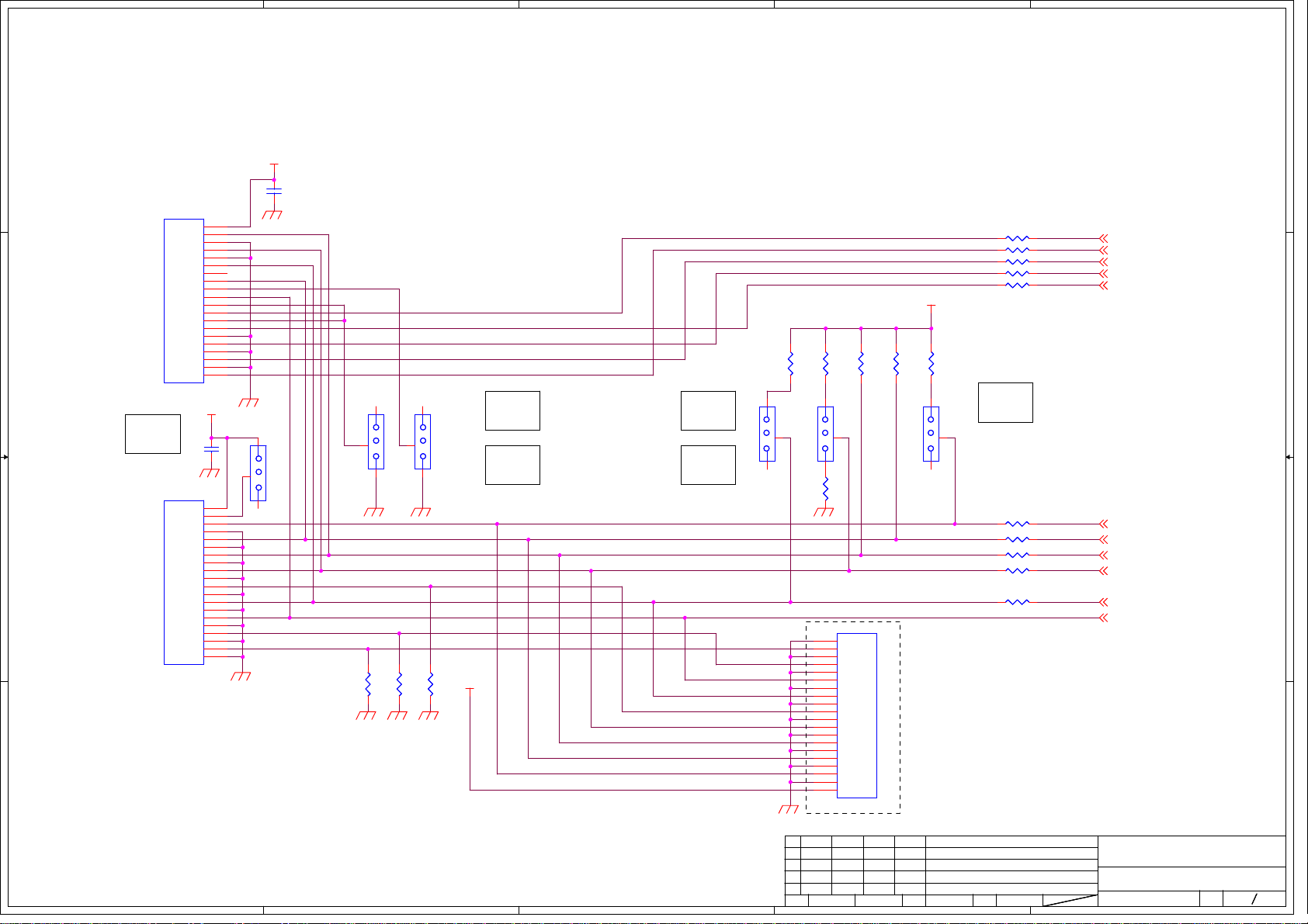
JTAG
(N.M.)
(Vsupply)
(5V/GND) (GNDdet)
(TCK)(TDO) (xTRST)
CN43
1-2 VCC
2-3 OPEN
CN38
1-2 OPEN
2-3 GND
CN39
1-2 OPEN
2-3 GND
CN40
1-2 PLUP
2-3 OPEN
CN41
1-2 PLUP
2-3 PLDN
CN42
1-2 PLUP
2-3 OPEN
R26 33
R26 33
CN8
FTSH-110-01-L-DV
CN8
FTSH-110-01-L-DV
18 18
11
12 12
19 19
16 16
10 10
88
99
66
33
11 11
17 17
77
15 15
14 14
55
44
20 20
13 13
22
R18
10K
R18
10K R22
10K
R22
10K
CN39CN39
13
2
C17
0.1uF
C17
0.1uF
CN9
FAP-20-08#4-0BF
CN9
FAP-20-08#4-0BF
GND 18
3.3V 1
GND 12
DBGACK 19
GND 16
GND 10
GND 8
TCK 9
GND 6
xTRST 3
RTCK 11
DBGRQ 17
TMS 7
xSRST 15
GND 14
TDI 5
GND 4
GND 20
TDO 13
3.3V 2
R30
10K
R30
10K
CN42CN42
13
2
C18
0.1uF
C18
0.1uF
R21
10K
R21
10K
R20
10K
R20
10K
R31
10K
R31
10K
CN38CN38
13
2
R25 33
R25 33
R39 33
R39 33
R28 33
R28 33
R24 33
R24 33
R40 33
R40 33
R43 33
R43 33
R19
10K
R19
10K
R27 33
R27 33
CN40CN40
13
2
CN41CN41
13
2
R42 33
R42 33
CN43CN43
13
2
CN17
SICA20C20Z-GA101
CN17
SICA20C20Z-GA101
18
18
1
1
12
12
19
19
16
16
10
10
8
89
9
6
6
3
3
11
11
17
17
7
7
15
15 14
14
5
54
4
20
20
13
13
2
2
R41 33
R41 33
R23
10K
R23
10K
R29
10K
R29
10K

5
5
4
4
3
3
2
2
1
1
D D
C C
B B
A A
MCUVCC USBVCC
VCC
VCC3
VCC5
VBUS
VCC5
VCC3
VCC
MCUVCC MCUVCC
USBVCC
MCUVCC
AVCC
VCC3
VCC5 VCC5
X0 [1,2]
X1 [1,2]
X0A [1,2]
X1A [1,2]
Ed.
Desig. Date Desig. Check Appr. Description
Title
Check Appr.
Draw.No.
Fujitsu Semiconductor Limited Sheet
FM3 Evaluation Board (LQFP-64/LQFP-120)
66
POWER,LED,SWITCH,CLOCK
Ed.
Desig. Date Desig. Check Appr. Description
Title
Check Appr.
Draw.No.
Fujitsu Semiconductor Limited Sheet
FM3 Evaluation Board (LQFP-64/LQFP-120)
66
POWER,LED,SWITCH,CLOCK
Ed.
Desig. Date Desig. Check Appr. Description
Title
Check Appr.
Draw.No.
Fujitsu Semiconductor Limited Sheet
FM3 Evaluation Board (LQFP-64/LQFP-120)
66
POWER,LED,SWITCH,CLOCK
Power
LED
MAIN CLK
Power Pin
SUB CLK
Power LED
Power Connect
Push SW
[32.768KHz]
[4MHz]
(EXT/VBUS)
(VCC3/5)
(USBVCC)
(MCUVCC)
(AVCC)
PWR
1-2 DC
2-3 VBUS
VCC
1-2 3V
2-3 5V
USBVCC
1-2 3V
2-3 5V
TP4
VCC
TP4
VCC
1
CN44CN44
13
2
C39
12pF/50V
C39
12pF/50V
R35
2K
R35
2K
C26
0.47uF
C26
0.47uF
TP6
VCC
TP6
VCC
1
C23
10uF
C23
10uF
C36
12pF/50V
C36
12pF/50V
D6
LED_2
D6
LED_2
C21
10uF
C21
10uF
CN45CN45
13
2
CN50CN50
1 2
SW6
B3SL-1002P
SW6
B3SL-1002P
1 2
CN47CN47
1 3
2
D3
P_LED
D3
P_LED
X1
CX1255GB0400H0PESZZ
X1
CX1255GB0400H0PESZZ
1
2 3
4
CN49CN49
1
3
2
4
C19
0.1uF
C19
0.1uF
+
C20
100uF
+
C20
100uF
C35
12pF/50V
C35
12pF/50V
TP9
GND
TP9
GND
1
CN48CN48
1 3
2
R46
0
R46
0
CN46CN46
1 3
2
R33
10k
R33
10k
TP3
GND
TP3
GND
1
C38
12pF/50V
C38
12pF/50V
R38
2K
R38
2K
TP8
GND
TP8
GND
1
X2
TFX-03 32.768KHz_12.5pF
X2
TFX-03 32.768KHz_12.5pF
1 2
C22
0.1uF
C22
0.1uF
C24
10uF
C24
10uF
R37
2K
R37
2K
TP7
GND
TP7
GND
1
D7
LED_3
D7
LED_3
R36
2K
R36
2K
M5
LT1963A-3.3
M5
LT1963A-3.3
OUT 4
SENSE 5
IN
1SHDN
2GND
3
TP2
UVCC
TP2
UVCC
1
R32
2K
R32
2K
D5
LED_1
D5
LED_1
TP5
GND
TP5
GND
1
C25
0.47uF
C25
0.47uF
R44
0
R44
0
R34
10k
R34
10k
TP1
VCC
TP1
VCC
1
CN21
HEC0470-01-630
CN21
HEC0470-01-630
1
3
2
D4
LED_0
D4
LED_0
SW5
B3SL-1002P
SW5
B3SL-1002P
1 2
FM3-64SD1NQ
FM3-120SD1NQ
01 版
中華人民共和国「電子情報製品汚染防止管理弁法」の対応
Compliance with Administration on the Control of Pollution Caused by Electronic Information Products
of the People’s Republic of China
电子信息产品污染控制管理办法(第 39 号)
产品中有毒有害物质或元素的名称及含量
部件名称
铅
汞
镉
六价铬
多溴联苯
多溴二苯醚
(Pb) (Hg) (Cd) (Cr(Vl)) (PBB) (PBDE)
印刷线路板 × ○ ○ ○ ○ ○
2012/3/23 作成
All rights reserved,Copyright ©2013 東京エレテック
株式会社
有毒有害物质或元素
○:表示该有毒有害物质在该部件所有均质材料中的含量均在 SJ/T11363-2006 規定的限量要求以下。
×:表示该有毒有害物质至少在该部件的某一均质材料中的含量超出 SJ/T11363-2006 規定的限量要求。
这标记是按照 2006 年 2 月 28 日公布的[电子信息产品污染控制管理办
法]以及 SJ/T11364-2006[电子信息产品污染控制标识要求]在中国销售
的电子信息产品的环保使用期限。如遵守关于这产品的安全或使用上的
注意,在这期限内(从生产日期起算)不会因产品中的有害物质漏到外
部,或发生突然变异,而引起环境污染和对人体或财产的重大影响。
This manual suits for next models
1
Other TOKYO ELETECH Motherboard manuals


Popular Motherboard manuals by other brands

Asus
Asus SABERTOOTH X79 user manual

VIA Technologies
VIA Technologies VX800 Series Technical manual

International Rectifier
International Rectifier IRS27951 user guide

Gigabyte
Gigabyte GA-8ID2003 user manual

ASROCK
ASROCK X58 EXTREME6 - brochure

Infineon
Infineon MERUS EVAL-AUDIO-MA2304DNS-B quick start guide


