TOKYO ELETECH FM0+64SD1NQ User manual

2015/3/25 TOKYO ELETECH
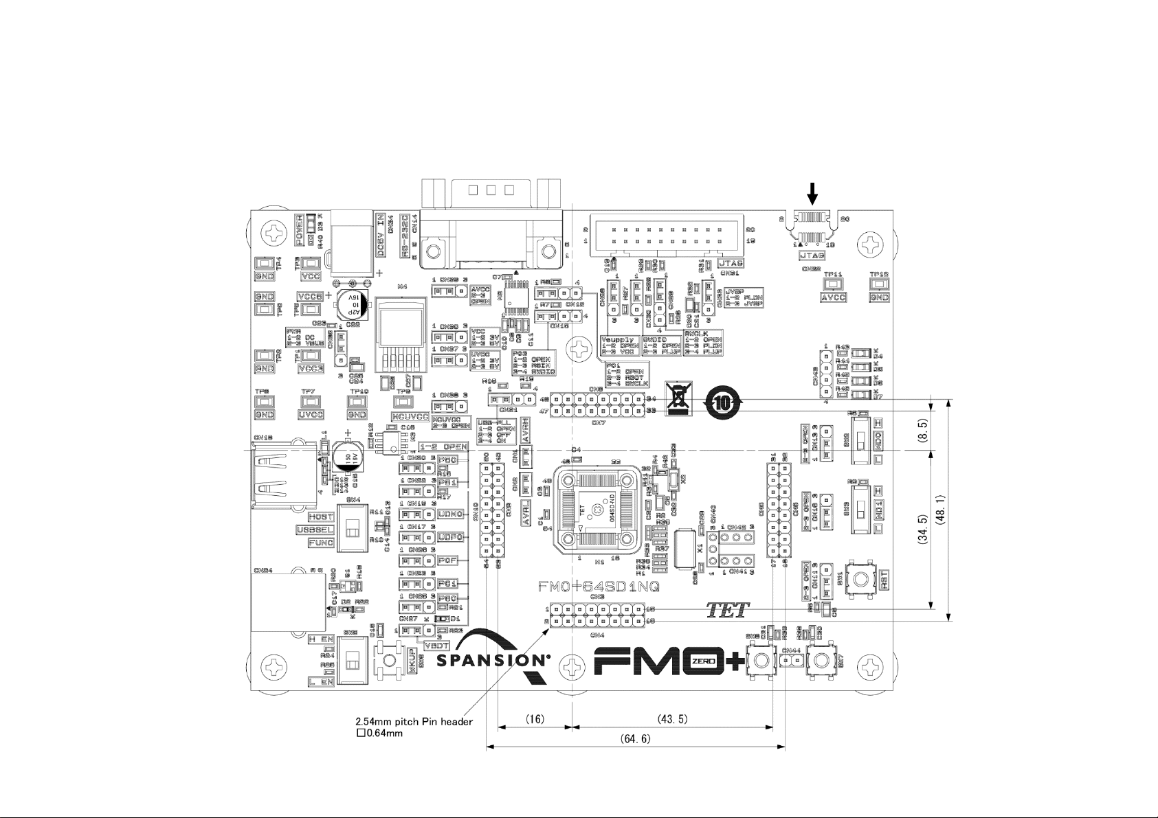
FM0+64SD1NQ
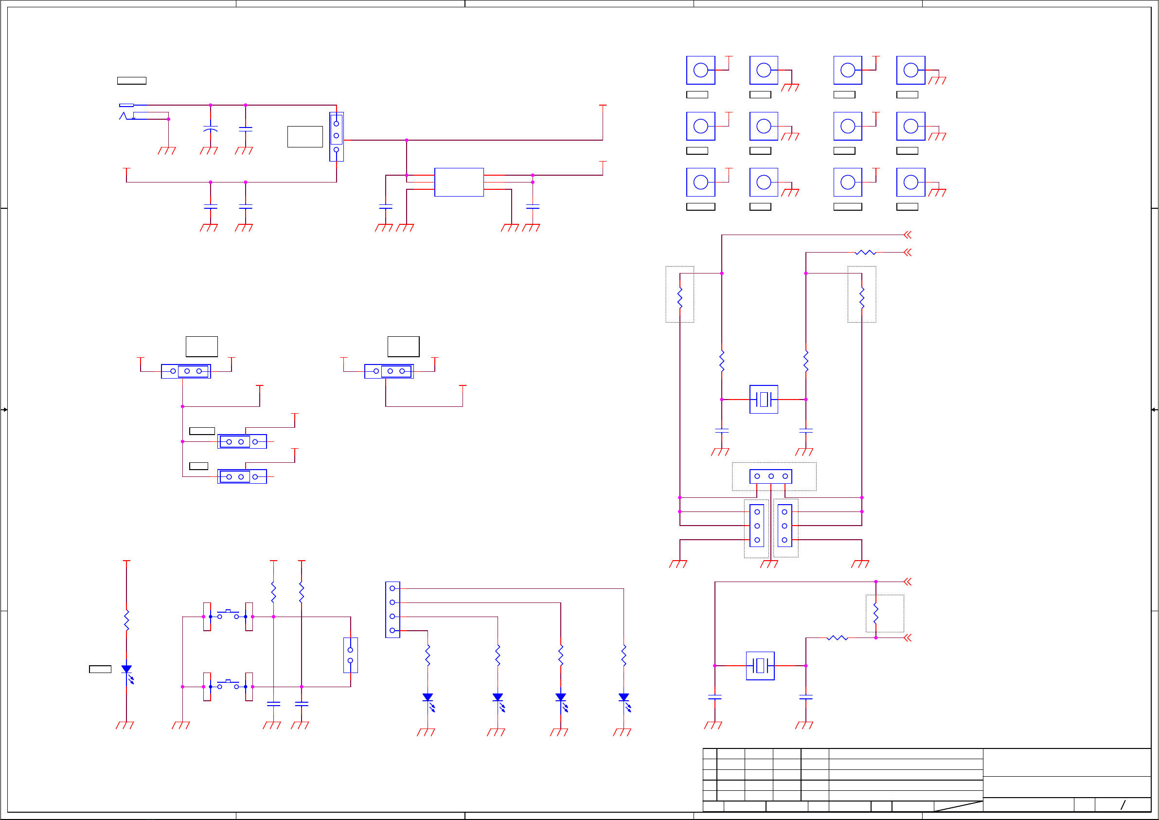
1. Power supply selection (Note: * default setting)
POWER SOURCE
CN28 CN33 CN35
DC 5V 1-2* 1-2* 1-2*
USB VBUS 1-2 1-2 2-3
JTAG V-supply 1-2 2-3 Open
VCC SELECTION
CN36 CN37 CN38 CN39
3.3V 1-2* 1-2* 1-2* 1-2*
5V 2-3 2-3 1-2 1-2
2. Switch, Jumper Pin Settings (Note: * default setting)
FUNCTION SETTING ACTION
SW1 RESET SWITCH PUSH ON RESET
PUSH OFF NOT RESET
SW2 MD0 1-2 HIGH
2-3* LOW
SW3 MD1 1-2 HIGH
2-3* LOW
SW4 USB SELECTION 5-6 2-3 USB HOST
4-5 1-2* USB FUNC
SW5 WKUP LEVEL SWITCH 5-6 2-3 H ENABLE
4-5 1-2* L ENABLE
SW6 (NO MOUNT) - -
SW7 (OPTIONAL) - -
SW8 (OPTIONAL) - -
CN1 AVRH 1-2* CONNECT TO AVCC
CN2 AVRL 1-2* CONNECT TO AVSS
CN11 INITX
1-2* CONNECT TO RESET SWITCH
2-3 OPEN
CN12 SOT (UART TX) 1-2* OPEN
2-3 CONNECT TO RS TRANSCEIVER
3-4 CONNECT TO SWD I/F (SWCLK)
2015/3/25 TOKYO ELETECH
CN13 MD0 1-2* CONNECT TO MD0 SWITCH
2-3 OPEN
CN15 SIN (UART RX) 1-2* OPEN
2-3 CONNECT TO RS TRANSCEIVER
3-4 CONNECT TO SWD I/F (SWDIO)
CN16 MD1 1-2* CONNECT TO MD1 SWITCH
2-3 OPEN
CN17 UDP0 (USB D+) 1-2* OPEN
2-3 CONNECT TO USB CONNECTOR
CN19 UDM0 (USB D-) 1-2* OPEN
2-3 CONNECT TO USB CONNECTOR
CN20 P50 1-2* OPEN
2-3 CONNECT TO VBUS CONTROL IC FLG
CN21 P22 (USB-PLL) 1-2* OPEN
2-3 USB PLL OFF
3-4 USB PLL ON
CN22 P51 1-2* OPEN
2-3 CONNECT TO VBUS CONTROL IC EN
CN23 P61 1-2* OPEN
2-3 CONNECT TO USB D+ PULL-UP CONTROL
CN25 P60 (USB CONN. DET.) 1-2* OPEN
2-3 CONNECT TO USB VBUS
CN26 P0F 1-2* DO NOT USE WKUP SW (SW6)
2-3 USE WKUP SW (SW6)
CN27 TEST CONNECTOR 1-2* DO NOT USE USB
2-3 USE USB
CN29 SWCLK 1-2* OPEN
2-3 PULL-DOWN
3-4 PULL-UP
CN30 SWDIO 1-2* OPEN
2-3 PULL-UP

2015/3/25 TOKYO ELETECH
Revision history:
2015/3/25 Initial revision
The following precautions apply to the product described in this manual.
Before moving the product, be sure to turn off all the power supplies and unplug the cables. Watch your step when carrying the
product. Do not use the product in an unstable location such as a place exposed to strong vibration or a sloping surface.
Do not place anything on the product or expose the product to physical shocks. Do not carry the product after the power has
been turned on. Doing so may cause a malfunction due to overloading or shock.
Since the product contains many electronic components, keep it away from direct sunlight, high temperature, and high humidity
to prevent condensation. Do not use or store the product where it is exposed to much dust or a strong magnetic or electric field
for an extended period of time. Inappropriate operating or storage environments may cause a fault.
Use the product within the ranges given in the specifications. Operation over the specified ranges may cause a fault.
To prevent electrostatic breakdown, do not let your finger or other object come into contact with the metal parts of any of the
connectors. Before handling the product, touch a metal object (such as a door knob) to discharge any static electricity from your
body.
Always turn the power off before connecting or disconnecting any cables from the product. When unplugging a cable, unplug
the cable by holding the connector part without pulling on the cable itself. Pulling the cable itself or bending it may expose or
disconnect the cable core, resulting in a fault.
It is recommended that it be stored in the original packaging. Transporting the product may cause a damage or fault. Therefore,
keep the packaging materials and use them when re-shipping the product.
The contents of this document are subject to change without notice.
The information, such as descriptions of function and application circuit examples, in this document are presented solely for the
purpose of reference to show examples of operations and uses of Spansion Inc. and other vendors device; TOKYO ELETECH
and Spansion Inc. do not warrant proper operation of the device with respect to use based on such information. When you
develop equipment incorporating the device based on such information, you must assume any responsibility arising out of such
use of the information. TOKYO ELETECH and Spansion Inc. assume no liability for any damages whatsoever arising out of the
use of the information.
Any information in this document, including descriptions of function and schematic diagrams, shall not be construed as license
of the use or exercise of any intellectual property right, such as patent right or copyright, or any other right of TOKYO
ELETECH or any other right of Spansion Inc. or any third party or do TOKYO ELETECH and Spansion Inc. warrant
non-infringement of any third-party's intellectual property right or other right by using such information. TOKYO ELETECH
and Spansion Inc. assume no liability for any infringement of the intellectual property rights or other rights of third parties which
would result from the use of information contained herein.
The products described in this document are designed, developed and manufactured as contemplated for general use, including
without limitation, ordinary industrial use, general office use, personal use, and household use, but are not designed, developed
and manufactured as contemplated (1) for use accompanying fatal risks or dangers that, unless extremely high safety is secured,
could have a serious effect to the public, and could lead directly to death, personal injury, severe physical damage or other loss
(i.e., nuclear reaction control in nuclear facility, aircraft flight control, air traffic control, mass transport control, medical life
support system, missile launch control in weapon system), or (2) for use requiring extremely high reliability (i.e., submersible
repeater and artificial satellite). Note that TOKYO ELETECH and Spansion Inc. will not be liable against you and/or any third
party for any claims or damages arising in connection with above-mentioned uses of the products.
Any semiconductor devices have an inherent chance of failure. You must protect against injury, damage or loss from such
failures by incorporating safety design measures into your facility and equipment such as redundancy, fire protection, and
prevention of over-current levels and other abnormal operating conditions.
Exportation/release of any products described in this document may require necessary procedures in accordance with the
regulations of the Foreign Exchange and Foreign Trade Control Law of Japan and/or US export control laws.
The company names and brand names herein are the trademarks or registered trademarks of their respective owners.
USB VBUS
POWER
FM0+64SD1NQ (FIGURE EXAMPLE BELOW)
DC5V CN31 J AG
CN32 J AG
E SICA20C20Y-GA101
(NO MOUN ED)

5
5
4
4
3
3
2
2
1
1
D D
C C
B B
A A
AVRH
AVRL
MCUVCC
C
AVRL
AVRH AVCC
MCUVCC
P50[2,4]
P40[2] P41[2] P42[2] P43[2] P4C[2] P4D[2]
INITX[2,3,5]
P46/X0A[2,6] P47/X1A[2,6]
MD0[2,3] PE2/X0[2,6] PE3/X1[2,6]
P0F [2,4]
P05/MD1 [2,3]
P03 [2,3]
P80/UDM0 [2,4]
P81/UDP0 [2,4]
P60 [2,4]
P1E [2]
P1D [2]
P1C [2]
P1B [2]
P1A [2]
P1F [2]
P10 [2]
P11 [2]
P12 [2]
P13 [2]
P23 [2]
P22 [2,4]
P21 [2]
P00 [2]
P01 [2,3]
P02 [2]
P51[2,4] P52[2] P53[2] P30[2] P31[2] P32[2] P33[2] P34[2] P35[2] P3A[2] P3B[2] P3C[2] P3D[2] P3E[2] P3F[2]
P4E[2]
P0C [2]
P61 [2,4]
P0B [2]
P15 [2]
P14 [2]
Ed.
Desig. Date Desig. Check Appr. Description
Title
Check Appr.
Draw.No.
Spansion Inc. Sheet
FM0+ Evaluation Board (LQFP-64)
61
MCU or SOCKET
Ed.
Desig. Date Desig. Check Appr. Description
Title
Check Appr.
Draw.No.
Spansion Inc. Sheet
FM0+ Evaluation Board (LQFP-64)
61
MCU or SOCKET
Ed.
Desig. Date Desig. Check Appr. Description
Title
Check Appr.
Draw.No.
Spansion Inc. Sheet
FM0+ Evaluation Board (LQFP-64)
61
MCU or SOCKET
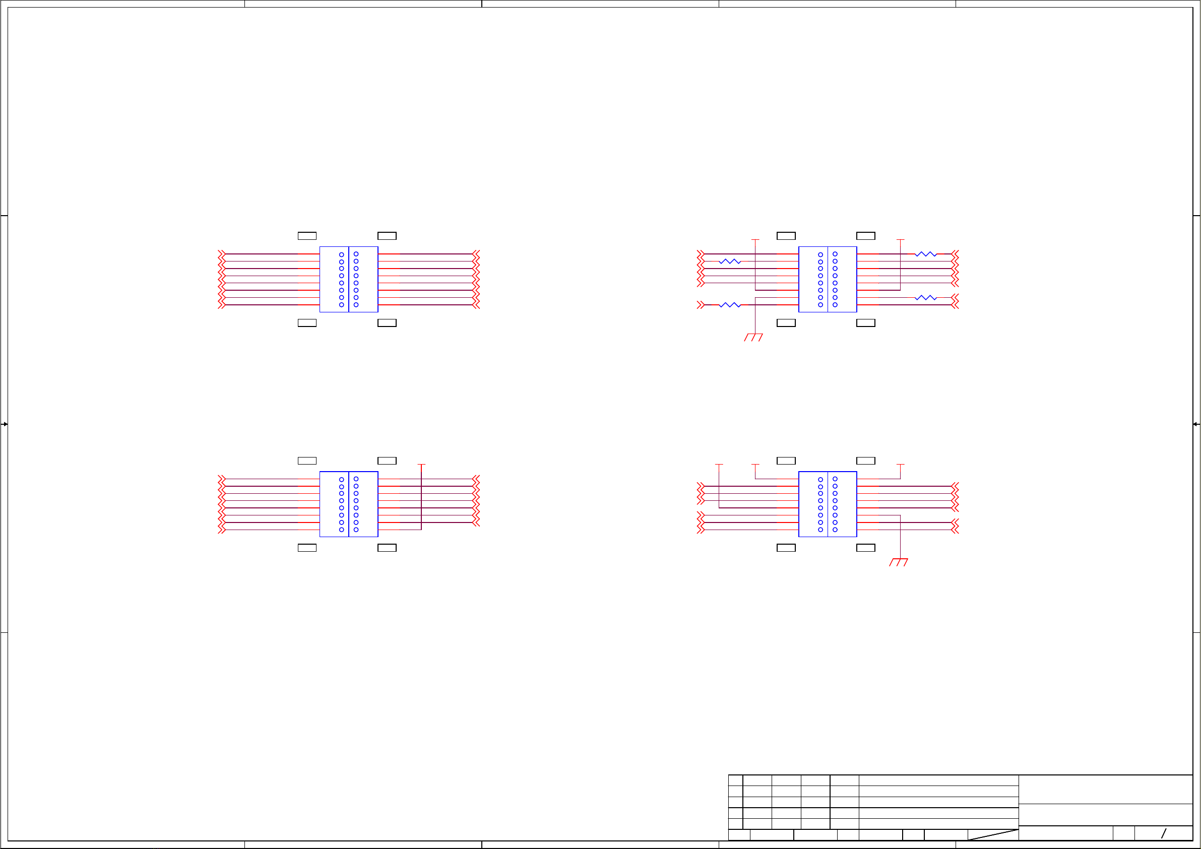
CN1
1 2
C1
0.1uF/10V
12
C4
0.1uF/10V
12
M1
FM0+_LQFP-64
P50/SIN3_1/INT00_0
1
P51/SOT3_1/INT01_0
2
P52/SCK3_1/INT02_0
3
P53/TIOA1_2/INT07_2
4
P30/SCS60_1/TIOB0_1/INT03_2/MI2SWS6_1
5
P31/SCK6_1/SI2CSCL6_1/INT04_2/MI2SCK6_1
6
P32/SOT6_1/SI2CSDA6_1/TIOB2_1/INT05_2/MI2SDO6_1
7
P33/ADTG_6/SIN6_1/INT04_0/MI2SDI6_1
8
P34/SCS61_1/TIOB4_1/MI2SMCK6_1
9
P35/SCS62_1/TIOB5_1/INT08_1
10
P3A/TIOA0_1/INT03_0/RTCCO_2/SUBOUT_2/IC1_CIN_0
11
P3B/TIOA1_1/IC1_DATA_0
12
P3C/TIOA2_1/IC1_RST_0
13
P3D/TIOA3_1/IC1_VPEN_0
14
P3E/TIOA4_1/IC1_VCC_0
15
P3F/TIOA5_1/IC1_CLK_0
16
MD0
17
PE2/X0
18
PE3/X1
19
P40/TIOA0_0/INT12_1
20
P41/TIOA1_0/INT13_1
21
P42/TIOA2_0
22
P43/ADTG_7/TIOA3_0
23
P4C/SCK7_1/TIOB3_0
24
P4D/SOT7_1
25
P4E/SIN7_1/INT06_2
26
VCC
27
C
28
VSS
29
P46/X0A
30
P47/X1A
31
INITX
32 P60/TIOA2_2/INT15_1/CEC1_0 33
P1E/RTS4_1/MI2SMCK4_1 34
P1D/CTS4_1/MI2SWS4_1 35
P1C/SCK4_1/MI2SCK4_1 36
P1B/SOT4_1/MI2SDO4_1 37
P1A/SIN4_1/INT05_1/CEC0_0/MI2SDI4_1 38
P1F/ADTG_5 39
P10/AN00 40
P11/AN01/SIN1_1/INT02_1/WKUP1 41
P12/AN02/SOT1_1 42
P13/AN03/SCK1_1/RTCCO_1/SUBOUT_1 43
P14/AN04/SIN0_1/SCS10_1/INT03_1 44
P15/AN05/SOT0_1/SCS11_1 45
P23/AN06/SCK0_0/TIOA7_1 46
P22/AN07/TIOB7_1 47
AVCC 48
AVRH 49
AVRL 50
P21/INT06_1/WKUP2 51
P00/WKUP4 52
P01/SWCLK/SOT0_0 53
P02/WKUP5 54
P03/SWDIO/SIN0_0/TIOB7_0 55
P05/MD1/TIOA5_2/INT00_1/WKUP3 56
VCC 57
P80/UDM0 58
P81/UDP0 59
VSS 60
P61/UHCONX0/TIOB2_2 61
P0B/TIOB6_1/WKUP6 62
P0C/TIOA6_1/WKUP7 63
P0F/NMIX/WKUP0/RTCCO_0/SUBOUT_0/CROUT_1 64
W1
C3
0.1uF/10V
12
C5
4.7uF/16V
12
W2
CN2
1 2
C2
0.1uF/10V
12
5
5
4
4
3
3
2
2
1
1
D D
C C
B B
A A
(Monitor 4)
(Monitor 1)1
15 1 6
2 17 18(Monitor 2)
31 3 2
33 34(Monitor 3)
47 4 8
49 5 0
63 6 4
MCUVCC
AVCC
C
AVRH AVRLMCUVCC
P51 [1,4]
P21[1]
MD0[1,3]
P01[1,3]
PE2/X0 [1,6]
INITX [1,3,5]
P10 [1]
P23 [1]
P1E [1]
P1C [1]
P1A [1]
P60[1,4] P1D[1] P1B[1] P1F[1]
P00 [1]
P81/UDP0[1,4]
P02 [1]
P53 [1]
P31 [1]
P33 [1]
P50[1,4] P52[1] P30[1] P32[1]
P47/X1A[1,6] P46/X0A [1,6]
P40 [1]
P12 [1]
P14 [1]
P11[1]
P15[1] P22[1,4]
P13[1]
P03[1,3] P05/MD1 [1,3]
P61[1,4] P0C[1] P0B [1]
P0F [1,4]
P34[1] P35 [1]
P3A[1] P3B [1]
P3C[1] P3D [1]
P3E[1] P3F [1]
PE3/X1[1,6] P41[1] P42 [1]
P43[1] P4C [1]
P4E [1]P4D[1]
P80/UDM0 [1,4]
Ed.
Desig. Date Desig. Check Appr. Description
Title
Check Appr.
Draw.No.
Spansion Inc. Sheet
FM0+ Evaluation Board (LQFP-64)
62
Monitor Pins
Ed.
Desig. Date Desig. Check Appr. Description
Title
Check Appr.
Draw.No.
Spansion Inc. Sheet
FM0+ Evaluation Board (LQFP-64)
62
Monitor Pins
Ed.
Desig. Date Desig. Check Appr. Description
Title
Check Appr.
Draw.No.
Spansion Inc. Sheet
FM0+ Evaluation Board (LQFP-64)
62
Monitor Pins
R4 0
1 2
R1 0
1 2
R2 0
1 2
R3 0
1 2
CN6
PSS-410156-08
18 18
20 20
22 22
24 24
26 26
28 28
30 30
32 32
CN4
PSS-410156-08
22
44
66
88
10 10
12 12
14 14
16 16
CN9
PSS-410156-08
49
49
51
51
53
53
55
55
57
57
59
59
61
61
63
63
CN7
PSS-410156-08
33
33
35
35
37
37
39
39
41
41
43
43
45
45
47
47
CN5
PSS-410156-08
17
17
19
19
21
21
23
23
25
25
27
27
29
29
31
31
CN3
PSS-410156-08
1
1
3
3
5
5
7
7
9
9
11
11
13
13
15
15
CN10
PSS-410156-08
50 50
52 52
54 54
56 56
58 58
60 60
62 62
64 64
CN8
PSS-410156-08
34 34
36 36
38 38
40 40
42 42
44 44
46 46
48 48

5
5
4
4
3
3
2
2
1
1
D D
C C
B B
A A
MODE SW
Reset SW
RST
MD0
H
L
H
L
MD1
RS-232C
(D-SUB 9pin)
SOT
1-2 OPEN
2-3 RSOT
3-4 SWCLK
SIN
1-2 OPEN
2-3 RSIN
3-4 SWDIO
RS-232C
VCC
VCC
VCC
VCCVCC VCC
P01[1,2]
P05/MD1 [1,2]
MD0 [1,2]
P03[1,2]
INITX [1,2,5]
SWCLK[5]
SWDIO[5]
Ed.
Desig. Date Desig. Check Appr. Description
Title
Check Appr.
Draw.No.
Spansion Inc. Sheet
FM0+ Evaluation Board (LQFP-64)
63
MODE, RESET, RS232C
Ed.
Desig. Date Desig. Check Appr. Description
Title
Check Appr.
Draw.No.
Spansion Inc. Sheet
FM0+ Evaluation Board (LQFP-64)
63
MODE, RESET, RS232C
Ed.
Desig. Date Desig. Check Appr. Description
Title
Check Appr.
Draw.No.
Spansion Inc. Sheet
FM0+ Evaluation Board (LQFP-64)
63
MODE, RESET, RS232C
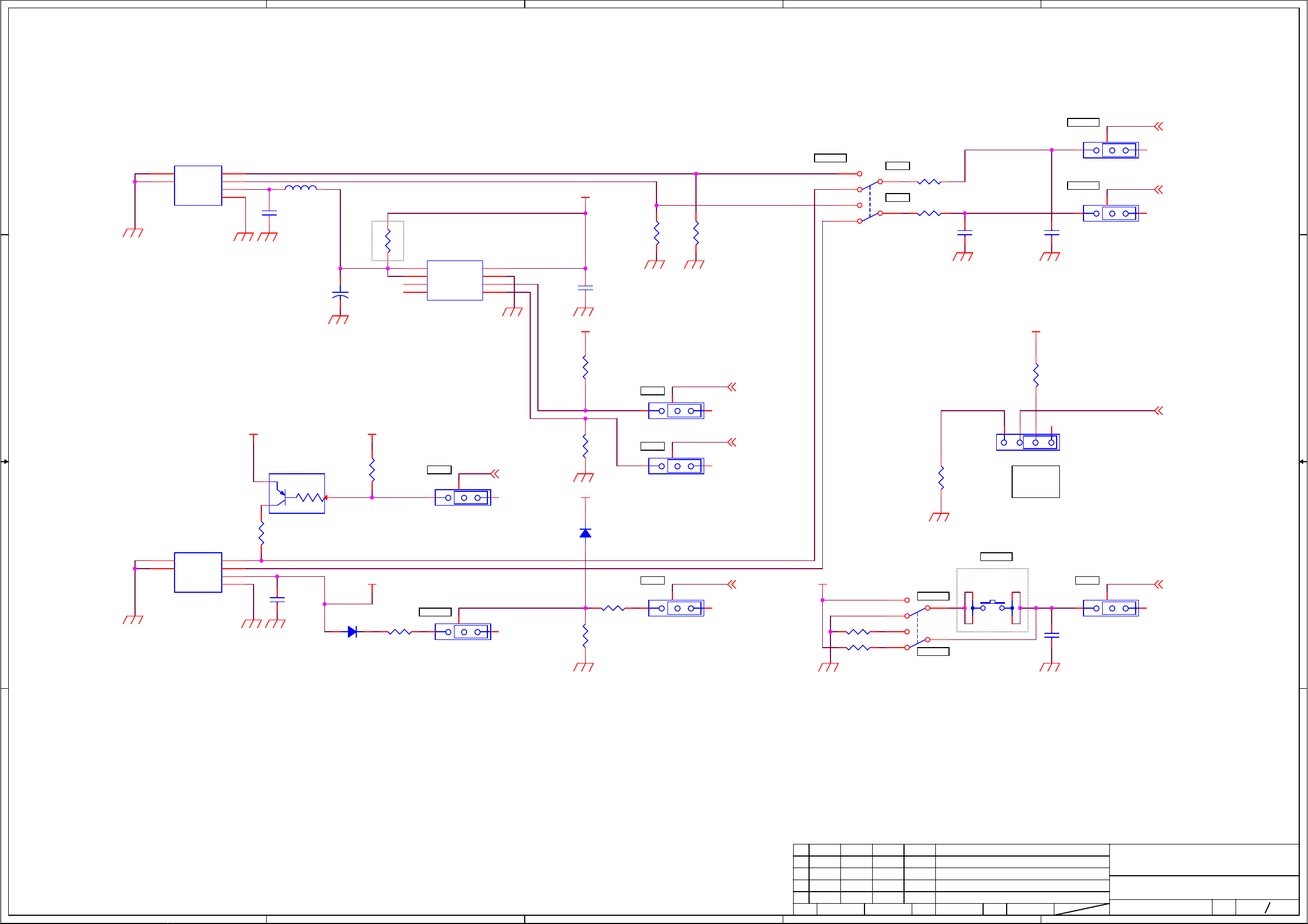
R7 4.7k
1 2
M2
MAX3232CUE+
C1+
1
V+
2
C1-
3
C2+
4
C2-
5V-
6
T2OUT 7
R2IN 8
R2OUT
9T2IN
10 T1IN
11
R1OUT
12
R1IN 13
T1OUT 14
GND 15
Vcc 16
CN16
1 3
2
R9 10k
1 2
SW1
B3SL-1002P
2 4
1 3
W5
CN14
RDEF-9PE-LNA(4-40)(50)
NC1
1
RXD
2
TXD
3
NC4
4
GND
5
NC6
6
RTS
7
CTS
8
NC9
9SHELL 10
SHELL 11
SW3
SS-12SDP2
2
1
3W7
R8 4.7k
1 2
C11
0.47uF/25V
12
C6
4.7uF/16V
12
CN15
1
3
2
4
SW2
SS-12SDP2
2
1
3
W4
R6 10k
1 2
CN11
1 3
2
C9
0.47uF/25V
12
R5 10k
1 2
W6
CN12
1
3
2
4
C7
0.1uF/10V
12
C10
0.47uF/25V
12
C8
0.1uF/10V
1 2
CN13
1 3
2
W3
5
5
4
4
3
3
2
2
1
1
D D
C C
B B
A A
(USB-A)
(USB-B)
H_D+
(N.M.)
F_D+
H_D-
F_D-
P0F
USB Host
USB Func
USB Func/Host
P61
VBDT
P60
UDP0
USBSEL HOST
FUNC
(N M )
(VBUS_FLG)
P50
P51
UDM0
(P61/UHCONX0)
(P0F/WKUP0)H EN
L EN
WKUP
USB-PLL
1-2 OPEN
2-3 OFF
3-4 ON
VCC5
VCC
UVCC VCC
VBUS
VCC
VCC VCC
P0F [1,2]
P81/UDP0 [1,2]
P80/UDM0 [1,2]
P50 [1,2]
P51 [1,2]
P61 [1,2]
P60 [1,2]
P22 [1,2]
Ed.
Desig. Date Desig. Check Appr. Description
Title
Check Appr.
Draw.No.
Spansion Inc. Sheet
FM0+ Evaluation Board (LQFP-64)
64
USB
Ed.
Desig. Date Desig. Check Appr. Description
Title
Check Appr.
Draw.No.
Spansion Inc. Sheet
FM0+ Evaluation Board (LQFP-64)
64
USB
Ed.
Desig. Date Desig. Check Appr. Description
Title
Check Appr.
Draw.No.
Spansion Inc. Sheet
FM0+ Evaluation Board (LQFP-64)
64
USB
SW6
B3SL-1002P
2 4
1 3
W14
R13 15k
1 2
CN25 13
2
R20 1.5k
1 2
W15
R25 10k
1 2
R19 10k
1 2
R23 10k
12
R16 10k
1 2
R10
27
1 2
C13
47pF/50V
12
R15 10k
12
CN23 13
2
W8
SW4
SS-22SDP2
2
1
3
5
4
6
C17
0.1uF/10V
12
CN17
13
2
CN21
1
3
2
4
R17 10k
12
W9
C18
0.47uF/25V
12
R18 100k
1 2
M3
LM3525M-H
IN 7
FLG 2
EN 1
GND 3
OUT
6
OUT
8
NC
4
NC
5
CN20 13
2
CN26 13
2
R22
3.6k
1 2
W10
10K
Q1
DTA114TUA
3
1
2
SW5
SS-22SDP2
2
1
3
5
4
6
R14 15k
1 2
D1
1SS390TE61
12
W12
R21
20k
1 2
CN18 87520-0010BLF
D+ 3
Vbus 1
GND 4
D- 2
CASE
5
CASE
6
D2
1SS390TE61
12
CN27 13
2
L1
MPZ2012S300A
1 2
W13
W11
C14
47pF/50V
12
CN19
13
2
+C15
150uF/16V
12
R24 10k
1 2
C12
0.1uF/10V
12
W16
R11
27
1 2
R12 0
1 2
CN24 61729-0010BLF
D+ 3
Vbus 1
GND 4
D- 2
CASE
5
CASE
6
C16
0.1uF/10V
12
CN22 13
2

5
5
4
4
3
3
2
2
1
1
D D
C C
B B
A A
JTAG
SWDIO
1-2 OPEN
2-3 PLUP
1-2 PLDN
2-3 JVSP
JTAG
JTAG
(N.M.)
SWCLK
1-2 OPEN
2-3 PLDN
3-4 PLUP
Vsupply
1-2 OPEN
2-3 VCC
(P03/SWDIO)
(P01/SWCLK)
JVSP
JVSP
VCC
JVSP
VCC
VCC5
INITX [1,2,3]
SWCLK [3]
SWDIO [3]
Ed.
Desig. Date Desig. Check Appr. Description
Title
Check Appr.
Draw.No.
Spansion Inc. Sheet
FM0+ Evaluation Board (LQFP-64)
65
JTAG
Ed.
Desig. Date Desig. Check Appr. Description
Title
Check Appr.
Draw.No.
Spansion Inc. Sheet
FM0+ Evaluation Board (LQFP-64)
65
JTAG
Ed.
Desig. Date Desig. Check Appr. Description
Title
Check Appr.
Draw.No.
Spansion Inc. Sheet
FM0+ Evaluation Board (LQFP-64)
65
JTAG
CN28
1 3
2
CN32
SICA20C20Z-GA101
18
18
1
1
12
12
19
19
16
16
10
10
8
89
9
6
6
3
3
11
11
17
17
7
7
15
15
14
14
5
5
4
4
20
20
13
13
2
2
R26 10k
12
R31 10k
12
CN30
1 3
2
W18
R27 10k
12
W19
C19
0.1uF/10V
12
CN33
13
2
C21
0.1uF/10V
12
CN29
1
3
2
4
W20
R32 10k
12
R28 10k
12
W17
R29 33
1 2
CN31
HIF3FC-20PA-2.54DSA(71)
GND 18
3.3V 1
GND 12
DBGACK 19
GND 16
GND 10
GND 8
TCK 9
GND 6
xTRST 3
RTCK 11
DBGRQ 17
TMS 7
xSRST 15
GND 14
TDI 5
GND 4
GND 20
TDO 13
3.3V 2
C20
10uF/10V
12
R30 33
1 2
5
5
4
4
3
3
2
2
1
1
D D
C C
B B
A A
VCC5
MCUVCC
VCC
UVCC
GND
GNDGND
GNDGND
PWR
1-2 DC
2-3 VBUS
VCC
1-2 3V
2-3 5V
UVCC
1-2 3V
2-3 5V
Power Pin
(N.M.)
(N.M.) (N.M.)
Power Connect
(EXT/VBUS)
(N.M.)
Power
Push SWPower LED
VCC3
LED
MAIN CLK
SUB CLK
DC5V IN
POWER
MCUVCC
AVCC
(N.M.) (N.M.)
AVCC GND
VCC3
VCC
VCC5
VBUS
VCC5
VCC3
VCC
MCUVCC
AVCC
UVCC
VCC
UVCC
VCC3VCC5
VCC
VCC3
MCUVCC
VCC
VCC5
AVCC
PE2/X0 [1,2]
PE3/X1 [1,2]
P46/X0A [1,2]
P47/X1A [1,2]
Ed.
Desig. Date Desig. Check Appr. Description
Title
Check Appr.
Draw.No.
Spansion Inc. Sheet
FM0+ Evaluation Board (LQFP-64)
66
POWER, LED, SWITCH, CLOCK
Ed.
Desig. Date Desig. Check Appr. Description
Title
Check Appr.
Draw.No.
Spansion Inc. Sheet
FM0+ Evaluation Board (LQFP-64)
66
POWER, LED, SWITCH, CLOCK
Ed.
Desig. Date Desig. Check Appr. Description
Title
Check Appr.
Draw.No.
Spansion Inc. Sheet
FM0+ Evaluation Board (LQFP-64)
66
POWER, LED, SWITCH, CLOCK
W25
C32
12pF/50V
12
R39 10k
12
TP6
1
CN44
1 2
CN40
1
3
2
CN42
1
3
2
R36 0
1 2
X1
8MHz
1 2
TP2
1
CN39
1 3
2
X2
32.768kHz
1 2
TP1
1
R34
0
1 2
D4
SML-210VTT86
21
SW7
B3SL-1002P
2 4
1 3
C33
12pF/50V
12
CN37
13
2
C31
0.47uF/25V
12
TP3
1
D3
SML-210PTT86
21
TP8
1
D5
SML-210VTT86
21
W23
CN34
HEC0470-01-630
1
3
2
SW8
B3SL-1002P
2 4
1 3
TP11
1
C30
0.47uF/25V
12
R43 330
1 2
R35
0
1 2
C24
10uF/10V
12
CN41
1
3
2
CN36
13
2
D6
SML-210VTT86
21
TP10
1
CN35
13
2
C25
0.1uF/10V
12
TP12
1
M4
LT1963AEQ-3.3#PBF
OUT 4
SENSE 5
SHDN
1
IN
2
GND
3TAB 6
R44 330
1 2
TP7
1
W21
CN43
1
3
2
4
D7
SML-210VTT86
21
R42 0
1 2
R38 10k
12
C28
12pF/50V
12
C23
0.1uF/10V
12
R45 330
1 2
C27
10uF/10V
12
R33 0
1 2
TP9
1
TP5
1
+
C22
100uF/16V
12
W22
TP4
1
CN38
1 3
2
C29
12pF/50V
12
R41
0
12
W24
R46 330
1 2
C26
10uF/10V
12
R40 330
1 2
R37 0
1 2
FM0+64SD1NQ
Rev.01
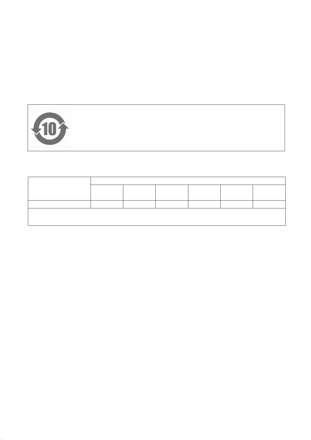
中華人民共和国「電子情報製品汚染防止管理弁法」の対応
Compliance with Administration on the Control of Pollution Caused by Electronic Information Products
of the People’s Republic of China
电子信息产品污染控制管理办法(第 39 号)
产品中有毒有害物质或元素的名称及含量
部件名称
铅
汞
镉
六价铬
多溴联苯
多溴二苯醚
(Pb) (Hg) (Cd) (Cr(Vl)) (PBB) (PBDE)
印刷线路板 × ○ ○ ○ ○ ○
2015/3/25
All rights reserved,Copyright ©2015 TOKYO ELETECH CORPORATION
有毒有害物质或元素
○:表示该有毒有害物质在该部件所有均质材料中的含量均在 SJ/T11363-2006 規定的限量要求以下。
×:表示该有毒有害物质至少在该部件的某一均质材料中的含量超出 SJ/T11363-2006 規定的限量要求。
这标记是按照 2006 年 2 月 28 日公布的[电子信息产品污染控制管理办
法]以及 SJ/T11364-2006[电子信息产品污染控制标识要求]在中国销售
的电子信息产品的环保使用期限。如遵守关于这产品的安全或使用上的
注意,在这期限内(从生产日期起算)不会因产品中的有害物质漏到外
部,或发生突然变异,而引起环境污染和对人体或财产的重大影响。
Other TOKYO ELETECH Motherboard manuals


