manuals.online logo
Brands
  1. Home
  2. •
  3. Brands
  4. •
  5. VESTEL
  6. •
  7. Plasma TV
  8. •
  9. VESTEL PL2000 User manual

VESTEL PL2000 User manual

Other VESTEL Plasma TV manuals

VESTEL 17MB11 User manual

VESTEL

VESTEL 17MB11 User manual

VESTEL 17MB15E-5 User manual

VESTEL

VESTEL 17MB15E-5 User manual

Popular Plasma TV manuals by other brands

Sony WEGA KE-P42M1 Service manual

Sony

Sony WEGA KE-P42M1 Service manual

LG 60PA5500 Specifications

LG

LG 60PA5500 Specifications

VisionQuest PVQ-32VGB owner's manual

VisionQuest

VisionQuest PVQ-32VGB owner's manual

LG PJ550N Specifications

LG

LG PJ550N Specifications

Samsung PA43H4000 user manual

Samsung

Samsung PA43H4000 user manual

LG 42LG70ER owner's manual

LG

LG 42LG70ER owner's manual

Samsung 7+ series quick start guide

Samsung

Samsung 7+ series quick start guide

Panasonic Viera TH-37PA60EY operating instructions

Panasonic

Panasonic Viera TH-37PA60EY operating instructions

LG DU-42PZ60H Service manual

LG

LG DU-42PZ60H Service manual

Panasonic Viera TH-42PX80A operating instructions

Panasonic

Panasonic Viera TH-42PX80A operating instructions

Panasonic VIERA TH-P50X30D Service manual

Panasonic

Panasonic VIERA TH-P50X30D Service manual

Samsung PS43F4510AW manual

Samsung

Samsung PS43F4510AW manual

Panasonic TH-50PX20U/P Service manual

Panasonic

Panasonic TH-50PX20U/P Service manual

Panasonic TH-37PW7BX operating instructions

Panasonic

Panasonic TH-37PW7BX operating instructions

Nexus NX422 owner's manual

Nexus

Nexus NX422 owner's manual

Panasonic TX-PR42U10 Service manual

Panasonic

Panasonic TX-PR42U10 Service manual

Panasonic TH42PV500EY operating instructions

Panasonic

Panasonic TH42PV500EY operating instructions

Panasonic Viera TH-50PE8U Service manual

Panasonic

Panasonic Viera TH-50PE8U Service manual

manuals.online logo
manuals.online logoBrands
  • About & Mission
  • Contact us
  • Privacy Policy
  • Terms and Conditions

Copyright 2025 Manuals.Online. All Rights Reserved.

PLASMA TV SERVICE MANUAL
We can separate plasma tv into parts of
•=Analog board: 11AN42Y
•=IR board: 11IR42Y
•=Digital board: 11DG42Y
•=Interface board: 11NEC42
•=Plasma display panel
•=Glass Filter
•=Mechanical parts: Chasis cover, back cover, front panel, IR box, and speaker
boxes
IR BOARD 11IR42Y
Ir board 11IR42Y is designed to place ir eye and two leds representing the
status of the TV.
ANALOG BOARD 11AN42Y
11AN42Y board is composed of 3 parts: Power part, IR part, Analog
part.
11AN42Y-Power Part
On the power part, the main voltages generated are (the followings are typical
voltages, you can see these voltages in detail in Adjustment part) :
Vs (Sustaining voltage) : 180V dc
Va (Addresing voltage) : 60V dc
Vaudio : 30V dc
Other voltages : 12, 5.1, 5, 3.3 V dc
12V and 5V dc are used on the analog and digital board in order to supply fans
and ICs. 3.3V dc is used to supply digital board ICs, which run with 3.3V.
5.1V dc is used to supply logic part (dsp, memory management, data driving,
multiplexing) of the plasma display panel.
Vaudio (30V dc) is used for audio amplifier TDA 7262 for audio output power
management.
Vs and Va are used for plasma display panel. Vs is to sustain the picture (colors)
on the screen and Va is to address the lines of the plasma display panel.
Power part of 11AN42Y can be separated into parts of
•=Stand-by power management,
•=PFC management,
•=12V management,
•=Va and Vaudio management,
•=Vs management,
•=Other voltages’ management
Stand-by power management is achieved with transformator L3 and a 5V
regulator LM7805.
PFC management, as a requirements of the norms, is achived with an active
solution. IC4 L4981B is used for active solution.
12V management includes both 12Vdc generation and 60V regulation. 12V
generation is achived with TR2.
Va and Vaudio generation is achieved by TR2. The regualtion os these
voltages are managed with IC6 TDA4605 and a regulation circuit around the IC.
Va voltage is also controlled by Vs voltage by a transistor circuit with T27
STP40N10. Adjustment of Va voltage is mentioned in Adjustments part.
Vs voltage is managed by IC2 SG3626 under control of Vrr voltage fed back
from plasma display panel. Along with transistors T1, T5 180V is generated
through L6. Adjustment of Vs voltage is mentioned in Adjustment part.
Other voltages’ management, 5.1V, 5V and 3.3V, are achieved by 2 regulator
ICs IC11, IC12 L4992.
11AN42Y- IR Part
IC3 AT90S1200A 8-bit microcontroller is used for
•=IR decoding : IR signal which is coming from ir board is processed
parallelly with main controller ST10 on digital board
•=Supply and driving of green and red leds: Leds are located on ir board
•=TV on/off : Drives relay REL1 and TV turns on or off
•=Helping Vrr voltage
11AN42Y- Analog Part
Anolog part can be divided into 2 parts Video processsing, which is managed
by VPC3215C-CIP3250A concept and Sound processing, which is managed by
MSP3410D-TDA8752.
Video signals have two similar paths since TV has PIP(Picture In
Picture)/PAP(Picture And Picture) features.
In order to make it easier to understand the explanations, video path without
PIP/PAP is called as Normal path, and the path with PIP/PAP is called PIP
path.
Video signals can be from Tuner, TUN1 CTT5000, 2 scarts PR6, PR4, and s-
vhs input PR5.
In TV mode, terresterial signal from tuner TUN1 is fed into IF box, IF1 IF3353,
and cvbs (composite video signal) from IF box is fed into VPC3215C, IC21 if the
path is normal or IC17 if it is PIP path.
Concerning scarts, cvbs is directly fed into VPC 3215C, IC21 if the path is
normal or IC17 if it is pip path.
Concerning s-vhs, Y(Luma)/C(Chroma) is fed into VPC 3215C, IC21 if the path
is normal or IC17 if it is pip path.
VPC3215C is a video processor which is used for color decoding, comb filtering,
sync processing and horizantal scaling and output formating. It is driven by a
20.25Mhz clock, X3.
Output video data signals, 8-bit Y and 8-bit C, from VPC3215C is fed into
CIP3250A, IC22 if the path is normal or IC18 if it is pip path.
CIP3250A is a component interface processor which is used for interfacing video
signals YUV coming from VPC315C, RGB signals from scart or teletext
processor, and then CIP3250A outputs digital 8-bit YUV signal in 4:2:2 format to
be fed into digital processing part on digital board.
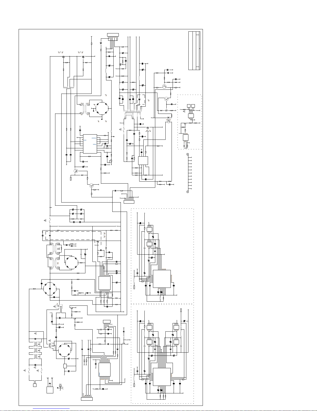
IC26 TPU3050, which is a teletext processor, is used as an RGB switch and
teletext processor along with IC27 GM76C8128, which is a memory IC. TPU3050
switches RGB signals from scart and output of teletext information.
Sound signals can be from IF box as sound IF and audio L, R signals from
scarts and audio sockets for pc and s-video inputs.
Sound processing is achieved by IC24 MSP3410D. It is driven by the xtal X4
18.432Mhz. Output of MSP3410D, which is audio L,R, is fed into IC13 TDA7262
for amplification of 2x15 watts on 4 ohm speakers.
MSP3410D also outputs 2 line out audio signals via PR14B on analog board.
DIGITAL BOARD 11DG42Y
Digital 8-bit YUV signals in 4:2:2 format are fed into GMVLX1A, IC14 if the path
is normal or IC1 if it is pip path.
GMVLX1A is used for de-interlacing, image scaling and gamma correction along
with KM4132G512A SGRAM, IC15 if the path is normal or IC2 if it is pip path.
Output of GMVLX1A is RGB each of 8-bit.
PC signal, which consists of analog RGB, horizantal and vertical syncronization
signals are fed into digital board via J2 DB15. Analog RGB signals are fed into
IC11 TDA8752, which is an analog to digital converter, in order to be converted
into digital 8-bit RGB.
According to the input mode selected, through buffer memories IC9, IC10 for PC
RGB and IC16, IC17 for normal video path, PC or normal video RGB and
syncronization signals are fed into IC18 GMFRC1A, which is a frame rate
conversion chip. PIP 8-bit RGB signal is fed into IC3 GMFRC1A for frame rate
conversion.
GMFRC1A manages frame rate conversion along with SDRAMs MT48LC1M16A
IC19, 20, 21 if the path is normal or IC4, 5, 6 if it is pip path.
After frame rate conversion process in GMFRC1As, video signals are fed into
IC22 EPF10K30AQC, which is a 30K size PLD (Programmable Logic Device).
This pld is used for digital board management and some special dsp applications
on video signal such as rounding, error diffusion. After PLD, video signal; RGB
each 8-bit with syncronization signals are ready to be sent to Plasma display
panel via Nec interface board.
OSD and menu managements are also carried out by this pld along with an osd
sdram IC23.
Main control of the TV is carried out by IC26 ST10R165 16-bit romless
microcontroller along with a flash ram of size 4Mbit, IC27 M29F040. Main
controller mainly manages analog board control and starts pld at the beginning.
INTERFACE BOARD 11NEC42
Note: This board is not used when plasma display panel is from FUJITSU-
HITACHI company.
Interface board is used to manage the interfacing between 68 pin connector and
80 pin connector. Through this board, the communication between main
controller ST10R165 and plasma display panel for some special applications
(such as PLE: Peak Luminance Enhancement) is achieved.
ADJUSTMENTS
If it Fujitsu
If it FujitsuIf it Fujitsu
If it Fujitsu-
--
-Hitachi panel,
Hitachi panel,Hitachi panel,
Hitachi panel,
Plasma Display TV has two important voltage adjustments and these
adjustments are related with plasma display panel. The voltages are, Vs (Panel
driver circuit voltage), and Va (Address driver circuit voltage).
These voltages are produced by 11AN42Y analog board power part. Vs and Va
are adjusted according to the feedback voltages from plasma display panel.
These feedback voltages are Vrr, Vrs, and Vra. According to these feedback
voltages, Va and Vs are adjusted via P1 and P2 potentiometers, respectively.
The following tables presents the settings of these voltage adjustments:
No. Item Symbol Term/Cond’n Value Unit
Min Typ. Max
1 Panel Driver Circuit
Voltage
Voltage Vs 165+10xVrs 165 - 185 V
Ripple/Noise Vnrs - - 500 mV
Stability - - - +/- 1.5 %
Setting accuracy - - - +/- 0,5 %
Current (average) Is APC function operation - - 1.5 A
Current (instant) Isp - - 12 A
2 Address Driver Circuit
Voltage
Voltage Va 55+10xVra 55 - 65 V
Ripple/Noise Vnrs - - 500 mV
Stability - +/- 1.5 %
Setting accuracy - +/- 0,5 %
Current (average) Ia - - 1.8 A
Current (instant) Iap - - 3.0 A
3 Logic Circuit Voltage
Voltage Vcc Fixed 4,75 5,0 5,25 V
Ripple/Noise Vnrs - - 200 mVp-p
Current (average) Icc - - 5.0 A
Current (instant) Icp - - 5.0 A
1. PDP unit will not operate under the following conditions. When in this
condition, panel driver circuit current “Is” will be less than 50mA.
•=“Vcc” has not been applied to the PDP unit.
•=2 second period from power on until all power supply voltages (Vs, Va,
and Vcc) have settled to normal operating levels.
•=“Vs” is outside of the standart range.
•=“Va” is outside of the standart range.
•=No vertical synchronous signal present at signal interface.
2. Reference voltage Vrs is the output from the PDP unit for “Vs” voltage setting.
3. Is current is automatically controlled to approximately 1.0A by the APC
(Automatic Power Control) function. However, at start-up (1 minute or less), it
can reach up to 4.0 A and then it goes down gradually to the convergent
value for about 3 minutes. The APC setting value on start-up is approximately
300W (APC start-up display load ratio is approximately 20%).
4. Reference voltage Vra is the output from the PDP unit for “Va” voltage setting.
5. Vrr is the sequence control voltage to Vs and Va. When Vrr is “Enable level”,
Vs and Va voltages are able to be input to the PDP unit. However, when Vrr
is “Disable level”, Vs and Va voltage should be deactivated.
No. Item Symbol Cond’n Value Unit
Min. Typ. Max.
1 Vs setting
voltage
Voltage
(variable) Vrs 0.0 - 2.0 V
Ripple/Noise Vnrr - - +/-500 mV
Stability
(average) - - - +/- 0.2 %
Current Irs - - 3 mA
2 Va setting
voltage
Voltage
(Variable) Vra 0.0 - 2.0 V
Ripple/Noise Vnrr - - +/-500 mV
Stability
(average) - - - +/- 0.2 %
Current Ira - - 3 mA
3 Sequence
conttrol high
voltage to Vs
and Va
Voltage
(Fixed) Vrr Enable
level
Disable
level
2.0
0.0
-
-
3.5
1
V
V
Ripple/Noise Vnrr - - +/-500 mV
Stability
(average) - - - +/- 0.2 %
Current Irr - - 3 mA
1. Vrs is set at a value obtained from the following formula which is relative to
Vs.
Vs= 165+10xVrs [Vrs: 0 to 2.0V]
2. Vra is set at a value obtained from the following formula which is relative to
Va.
Va=55+10xVra [Vra: 0 to 2.0V]
3. When the PDP-unit is powered on, Vrr is output at a value of about 0V. Then
if Vs and Va are able to be input to the PDP-unit from 11PWB42 board, Vrr is
output at a value of about 3.0V.
4. Load resistor for each output signal are set at a value of 1kohm.
If it NEC panel,
If it NEC panel,If it NEC panel,
If it NEC panel,
1. SUSTAIN POWER SUPPLY (Vs)
2. DATA POWER SUPPLY (Va)
3. LOGIC POWER SUPPLY
AUDIO_IN R
AUDIO
PC_IN
R
LINOUT_1 L
LINOUT_1 R
AUDIO
PC_IN L
LINOUT_2 L
LINOUT_2 R
Entrée
GAUCHE
Entrée
DROITE
Amplificateur
Audio 2x15W
HP-GAUCHE
HP-DROIT
Mute
Entrée
GAUCHE
Entrée
DROITE
Amplificateur2 Audio
2x15W
HP-GAUCHE
HP-DROIT
TUNER 2 ET FI 2
12V
Adaptateur
NEC
AUDIO_IN L
208070
ANALOG_HF FI AMPLI BF PL2
AMITEK
21, Rue Galilée
25Thursday, December 30, 1999
Fax 01 64 73 95 58
e_mail :[email protected]
77420 CHAMPS SUR MARNE
Tél 01 64 73 95 70
C
Title
Size Document Number Rev
Date: Sheet of
MUTE
peri_R
com_16/9
peri_G
SC3_in_r
peri_CR
audio_L
reset
SDA
C_svhs
SCL
SDA
Y_db25
peri_B
SC3_in_l
SCL
com_L
SCL
Y_svhs
audio_R
Y_peri
daca_l
SDA
daca_r
daca_l
reset
sv_peri2
sv_peri2
audio2_L
SDA
SCL
audio2_R
reset
I2s_in1
I2s_out
I2s_ws
I2s_cl
I2s_in1
I2s_out
I2s_ws
I2s_cl
Mute
audio_R
audio_L
audio2_R
audio2_L
+30V
SCL
SDA
Y_db25
+12V
Y_db25
Y_tv
daca_r
peri_on/off
gnd
+5V
gnd
g
gna
gna
gnd
gna g
+5V
gnd
gnd
gnd
gnd
gndgnd
gn
gna
gnd
gnd
gnd
gnd
gnd
gnd
gnd
gnd
gna
gnd
gnd
gnd
gndd
gna
gnd gnd
+5V
gnd
gnd
+60V
gnd
gna
gnd
gnd
gnd
gnd
gnd
gnd
gnd
gnd
+5V
gna
+12V
gnd
gnd
gnd
gnd
+5V
gn
gnd
g
+5V
gnd
gnd
gna
gnd
gnd
gnd
gnd
g
gna
gnd
+5V
ggna g
gn
gna
gnd
gnd
gndd
gna
gnd
gnd
gnd
gnd
+5V
gnd
gn
gnd
g
+5V
gnd
g
g
gndd gndd
gndd
g
gndd
g
gndd gndd
g
gndb
gndb
gndb
gndb
gndb
gndb
gndb
gndb
gndb
gndb
gndb
gndb
gndb
gndb
gndb gndb
gndb
gndb
gndb
gndb
gndb
gndb
gndb
gndb
gndb
gndb
gndb
gndb
gndb
gndb
gndb
gndb
gndbgndb
gndb
gndb
gndb
+30Vb
+30Vb
gndb
gndb
gnd
gnd
gnd
gnd
gnd
gnd
+5V
gnd
+33V
+33V
gnd
gnd
gn gn gn
gn
gna
gna
gna
+12Vc
+12Vc
+5V
gnd
gnd
gnd
gnd
gnd
+5Va
+5Va
+5Va
+5Va
gna
gna
gna
gna
gna
gna
gna
gna
gna gna
gna
gna
+5Va
+5Va
gnd
gnd
gnd
gnd
gnd
gnd
gnd
gnd
gnd
gnd
gnd
gnd
gnd
gnd
gnd
gnd
gnd
gnd
gnd
gnd
gnd
gnd
gnd
gnd
gnd
gnd
gnd
gnd
gnd
gnd
gnd
gnd
T32
2N7002
R121
33K
C328
100uF
25V
R200
10K
R207
10K
C346
100uF
25V
C287 1nF R196
10K
R307
100R
1/4W
C94
100nF
R315 100R
R227
1K
R323
22K
R109
100R
1/4W
C326
10uF
16V
R219
1K
IC29
DPL3519A
10
11
12
13
14
15
16
17
18
19
20
21
22
23
24
25
26
27
28
29
30
31
32
33
34
35
36
37
38
39
40
41
42
43
44
45
46
47
48
49
50
51
52
53
54
55
56
57
58
59
60
61
62
63
64
65
66
67
68
1
2
3
4
5
6
7
8
9
NC
STANBYQ
ADR_SEL
D_CTR_IO0
D_CTR_IO1
NC
NC
NC
AUD_CL_OUT
D_CTR_IN
XTAL_OUT
XTAL_IN
TESTEN
NC
NC
NC
AVSUP
AVSS
MONI_IN
VREFTOP
SC1_IN_R
SC1_IN_L
ASG1
SC2_IN_R
SC2_IN_L
ASG2
SC3_IN_R
SC3_IN_L
ASG4
NC
NC
NC
AGNDC
AHVSS
CAPL_C1
AHVSUP
CAPL_C2
SCI_OUT_L
SC1_OUT_R
VREF1
SC2_OUT_L
SC2_OUT_R
ASG3
NC
NC
NC
DACC1_L
DACC1_R
VREF2
DACC2_L
DACC2_R
RESETQ
NC
NC
I2S_DA_OUT2
I2S_DA_IN2
DVSS
DVSUP
NC
NC
NC
NC
I2S_DA_IN1
I2S_DA_OUT1
I2S_WS
I2S_CL
I2C_DA
I2C_CL
R226
68R
C204
10uF
16V
R324
68K
Z6
BZX84C
8V2
C314
33pF
R298
68R
R199
1K
C299
47uF
16V
C329
100nF
R126
2K7
C234
10uF
16V
R212
3K9
C217 47pF
R197 1K
R221 330R
R224
4K7
R336
68K
C102
100uF
25V
R327
100K
C221 1nF
R245
75R
C347
100nF
R325
22K
C311
1nF
R110
33K
R248
75R
C331
1nF
R250
75R
R234 470R
R233
75R
C317 1uF
50V
R105
1K5
C319
10nF
C200
2uF2
50V
R314
220R
J8
1
2
C201
2uF2
50V
R235 470R
C226
100uF
25V
C332
1nF
C236
1uF
50V
C257
390pF
R326
68K
C95
220pF
C318 22uF 16V
J16
1
2
3
4
5
6
7
8
9
10
11
12
C231
3uF3
50V
C325
100nF
T17
BC847B
C196
22uF
16V
R230
10K
R231
10K
C245
330pF
C313
220pF
C111
1000uF
50V
C303
2uF2
50V
L22
10uH
PR5
SVHS 4
3
2
1
5
6 7
C307
47uF
16V
T16
BC857B
L24
10uH
R353
10K
T23
BC847B
R386 10K
T20
BC847B
R252
75R
IC13
TDA7262
1
2
3
4
5
6
7
8
9
10
11
R292 470R
C320 33pF J18
1
2
3
T21
BC847B
J15
1
2
R96
1K5
R352
10K
R210
4K7
1/2W
R291
470R
C339
10pF
R385 10K R296
100K
R341
2K7
R108
1R
1/4W
R294 470R
L28
10uH
C304
1000uF 35V
C110
100nF
R348 100R
R371
10R
R297
100K
IC24
MSP3410D
{FOURNISSEUR}
{OBSERVATION}
10
11
12
13
14
15
16
17
18
19
20
21
22
23
24
25
26
27
28
29
30
31
32
33
34
35
36
37
38
39
40
41
42
43
44
45
46
47
48
49
50
51
52
53
54
55
56
57
58
59
60
61
62
63
64
65
66
67
68
1
2
3
4
5
6
7
8
9
NC
STANBYQ
ADR_SEL
D_CTR_OUT0
D_CTR_OUT1
NC
NC
NC
AUD_CL_OUT
DMA_SYNC
XTAL_OUT
XTAL_IN
TESTEN
ANA_IN2+
ANA_IN-
ANA_IN1+
AVSUP
AVSS
MONI_IN
VREFTOP
SC1_IN_R
SC1_IN_L
ASG1
SC2_IN_R
SC2_IN_L
ASG2
SC3_IN_R
SC3_IN_L
ASG4
SC4_IN_R
SC4_IN_L
NC
AGNDC
AHVSS
CAPL_M
AHVSUP
CAPL_A
SCI_OUT_L
SC1_OUT_R
VREF1
SC2_OUT_L
SC2_OUT_R
ASG3
NC
NC
NC
DACM_L
DACM_R
VREF2
DACA_L
DACA_R
RESQ
NC
NC
NC
I2S_DA_IN2
DVSS
DVSUP
S_CL
S_ID
NC
S_DA_IN
I2S_DA_IN1
I2S_DA_OUT
I2S_WS
I2S_CL
I2C_DA
I2C_CL
R306
1R
1/4W
R362
2K2
R118
6R8
{FOURNISSEUR}
4W
R331
470R
C223
100nF
R372
330R
C312
1uF
50V
R364
470R
R119
22K
C298
100uF
25V
R373
100K
R363
10K
TUN1
CTT5000
7
6
5
4
3
2
12
13
9
11
1
10
8
5VP
5VT
SDA
SCL
NC
NC
gnd
gnd
32V
IFO
AGC
gnd
gnd
R349 100R
R361
27K
C290
330nF
C294
330pF
M11
110066
{FOURNISSEUR}
1
2
R333
470R
R374
100K
C297
100nF
R107
33R
T29
BC857B
X4
18Mhz432
R369
1K
C218 47pF
C220 47pF
C291
330nF
C241
330nF
C295
330pF
R117
150K
PR4
PERITEL2
2
4
6
8
10
12
14
16
18
20
1
3
5
7
9
11
13
15
17
19
21
ED
MA
EG
CL
BUS
BUS
ML
CR
MC
EV
SD
SG
MB
B
MV
V
MR
R
MVI
SV
GND
C296
1000uF
35V
C242
330nF
C109
100nF
R321
100R
T35
BC847B
T13
BC847B
T28
BC857B
R293
100K
C305
100nF
R120
33K
R303
330R
R318
100R
1/4W
T36
BC847B
C244
22uF
16V
PR13B
CINCH
4
5
6
7
C243
22uF
16V
R124
4K7
R241
100K
R302
2K2
C199 1000uF
25V
R295
100K
R242
100K
T14
2N7002
C315 22uF 16V
L23 10uH
C225
100nF
PR13A
CINCH
1
2
3
8
R340
2K7
R376 10R
C216
470nF
C229
330nF
C212
100uF
25V
C235
100nF
J20
1
2
R97
33R
C302
100nF
R223 330R
C237
330nF
C228
220pF
C309
100uF
25V
T15
2N7002
R299
100R
C238
330nF
R320
33K
R378
330R
R238 470R
C239
330nF
R236 470R
C230
100nF
R99
100R
1/4W
C247
1nF
C308
2uF2
50V
C219
10uF
16V
R310
1K5
C248
1nF
R113
22K
X5
18Mhz432
C214
470nF
C222
10uF
16V
J14
1
2
R377
33K
C206 22uF 16V
C211
1nF
C224
10uF
16V
C208 22uF 16V
R290
470R
Z7
BZX85C
33V
C240
330nF
PAST8
1
C227
100pF
R114
68K
C207
10nF
R322
100R
C197
22nF
C232
1nF
C306
220pF
R350
100R
C209
10nF
C86
47uF
16V
L27
10uH
C198
100nF
R375
33K
R218
470R
C233
470nF
C202
1nF
R225
470R
R188
2K2
C203
1nF
R122
68K
R222
100K
R313 100R
T22
BC857B
R220
100R
1/2W
R351
100R
R228
100K
R115
22K
R304
6K8
T19
BC857B
R206 100R
C344
220nF
L21
10uH
R186
10K
C343
22pF
R191
6K8
R215
100R
C108 1uF
50V
R319
10K
R203
6K8
R217
100R
IC28
TDA7262
1
2
3
4
5
6
7
8
9
10
11
R106
220R
C301
22nF
R201
2K2
R204 100R
R301
1K5
C194
100uF
25V
R190
330R
T34
BC847B
R184
100R
R193
330R
R288
100R
R116
68K
R311
2K2
R317
1R
1/4W
C112
100nF
R312
6K8
C246
330pF
C323
100nF
R237
100K
R239
100K
R289
100R
C107
220pF
C300
22uF
16V
R243 5K6
C292
1nF
R232
75R
C97
47uF
16V
R300
10K
Z8
BZV55C
5V1
SZ1
BZX84C
8V2
R246
5K6
IC23
PCF8574T
13
15
14
1
2
35
12
11
10
7
9
6
4
8 16
INT
SDA
SCL
AO
A1
A2P1
P7
P6
P5
P3
P4
P2
P0
GND VCC
C193
100nF
R125
2K2
Z9
BZV55C
5V1
C293
1nF
C195 100nF
M13
110066
{FOURNISSEUR}
1
2
R149
150R
1/2W
J9
1
2
R335
100K
PR6
PERITEL
2
4
6
8
10
12
14
16
18
20
1
3
5
7
9
11
13
15
17
19
21
ED
MA
EG
CL
BUS
BUS
ML
CR
MC
EV
SD
SG
MB
B
MV
V
MR
R
MVI
SV
GND
C252
100nF
IF1
IF3353
1
2
3
4
5
6
7
8
9
10
11
13
14
15
16
IF IN
B/G
L
NORM
TUN AGC
CVBS
AF AM
AFC
SOUND IF
12V
5V
gnd
gnd
gnd
gnd
R316
33R
C310
1nF
C253
100nF
PR14A
CINCH
1
2
3
8
R181 330R
PAST7
1
R182 330R
R127
2K7
R189 1K
C93
1000uF 35V
R308
330R
R244
5K6
C322
100nF
R192 1K
C321
10uF
16V
T24
BC847B
R194 1K
R187 1K
R98
1R
1/4W
C2881uF 50V
C215
22pF
T30
BC847B
R213
100R
R185 1K
C104
1uF
50V
C316
10nF
C205
10pF
R229
15K
R211
100R
R334
33K
C210 10pF
R208
33R
R240
75R
R183
1K
R384
10K
R123
100K
C2891uF 50V
R209
2K2
C81
100nF
R309
10K
R214
330R
T31
2N7002
C327
100nF
R216
330R
R198
22K
PR14B
CINCH
4
5
6
7
C286 1nF
R202
22K
R205
10K
R305
33R
C76
1000uF
35V
C8
2uF2
50V
+12V
+12V
In 220AC N
F1
S1
S2
F2
S3
F3
0V gnd
Entrée
Secteur
venant
de
l'inter
In 220AC N
Alimentation
Digital Alimentation
Plasma
2
165
43
OUT 60V
Régulation de température
IR
LED
Entrée
Secteur
vers
l'inter
Prise avec filtre secteur
208070
ANALOG_ALIMENTATION PL2
AMITEK
21, Rue Galilée
15Thursday, December 30, 1999
Fax 01 64 73 95 58
e_mail :[email protected]
77420 CHAMPS SUR MARNE
Tél 01 64 73 95 70
C
Title
Size Document Number Rev
Date: Sheet of
VRR
VRA
VRS
Out_12V
A_RESET
IR_OUT
+30V
A_OFF_CLK
A_MOSI
A_MISO_IR
peri_on/off
+5 IR
440V
0V
+180V
440V
+60V
0V
0V
0V 0V
gnd
gnd
gnd
gnd
gnd
gnd
gnd
gnd
gnd
gnd
gnd
gnd
gnd
gnd
gnd
gnd
gnd
gnd
gnd_2
gnd
gnd
gnd
gnd_1
gnd
gnd
gnd
+5 IR
gnd
gnd
+12V
+5 IR
+5 IR
+5 IR
+12V
+5 IR
+12V
+12V
gnd
gnd_1
g
gndb
gnd
+5V
0V
gnd
sgnd
gnd
0V
0V
gnd_2
gnd_2
gnd_2
12Vb
gnd
gnd
gnd 60V
gnd_2
+5V
gndb
gnd
gnd 60V
12Va
gn
gnd
gnd
0V
gna
0V
+5.1V
gnd
0V
gnd
gnd
gnd
gnd
0V0V
12Va
gnd
gnd_1
gndd
0V
gnd
gnd
0V
12Va
+5.1V
12Vb
gnd
gnd_1
0V
0V
gnd
gnd
gnd_1
gnd_2
gnda
0V
0V
gnd_1
gnd
0V
gnd
gnd
gnd
+180V
REL1
RELAI 1RT
12
3
A2
A1
L29
42V32
3
67
2
R277
150K
1/2W
Z4 STPS5L25B
C278
100uF
25V
R346
33R
C280
100nF
C10
47uF
25V
F4
4AT
T11
BC847B
D9
1N4007
C85
100uF
25V
C47 18nF 630V
C281 100nF
R79
4K7
C337
1uF
250V
R276 1M
D36
BAS16
F3
4AT
R260
4K7
R62
39K 2W
C34
220uF
200V
C333
220nF
100V
C279
1000uF
35V
M16
110067
1
L13 47uH
T26
BC847B
D57
1N4007
C60
220nF
Z10
BZV85C
15V
D49 BAS16
1
Z2
BZV55C
5V1
D1
BY255
R284
470R
R95
20mR
M18
110067
1
D7
1N4007
C27
100nF
Z11
BZV55C
5V1
C70
2200uF
10V
C29
220pF
P3
1K
T7
BC847B
R81
4K7
R67
330K
1W
C276
470nF
250V
M17
110067
1
D51
BAS16
R258
4K7
D56
BAS16
R93
270R
R347
4K7
D13 BAS16
R78
220R
D17 BAS16
C75 10nF
D33 BYV28
200V
C284
10nF
M15
110067
1
IC11
L4992
1
32
2
3
4
5
6
7
8
9
10
11
12
13
14
15
16
17
18
19
20
21
22
23
24
31
30
29
28
27
26
25
H5STR
H5GA
VIN
REG5
V5SW
V5SNS
I5SNS
COMP5
SOFT5
CRST
PWROK
RUN5
VREF
SGND
NOSKIP
OSC
RUN3
SOFT3
COMP3
I3SNS
V3SNS
V131N
REG12
(*)
H3STR
H5SRC
R5GA
PGND5
PGND3
R3GA
H3SRC
H3GA
R259
4K7
D5
BY255
R101
1M
R103
1M
R86
1K
1
L12 47uH
D32
BA159
M19
110067
1
L14
47uH
C9
100nF
T3
BC847B
R343
12K
Z3 STPS5L25B
C17
470uF
250V
IC1
LM7805
2
13
G
IO
Z5 STPS5L25B
C57
100pF
1KV
1
R279
39K 2W
C80 10nF
R368
470R
D53 BA159
R5 100K 1/4W
C84
100uF
25V
L11
47uH
D26
MUR1560
C98
100uF
25V
L7
47uH
D14
1N4007
R47
120K
D35
BAS16
R66
470K
1W
C54
1000uF
16V
R46
5K6
D37
BAS16
C345
100nF
D29 MUR1560
200V/3A
R380
10K
C12
470uF
250V
R87
10K
D45 BAS16
R33
10K
C45
100uF
100V
R365 4K7
R280
39K 2W
R39
1K
R24
220R
F1
T4AH
R48
150K
R282
270K
1W
R94
20mR
R379
33K
D24
BAS16
F2
T4AH
R111
20mR
R283
33K
1/4W
C6
1nF
1KV
R366 4K7
C68
2200uF
10V
R381
27K
R90
470R
C26
100nF
R26
6K8
R29 470R
D4
BY255
C21
10nF
C105
2200uF
10V
T37
BC847B
R31 470R
C30
100pF
J2
1
2
C338
1uF
50V
C22 100nF
R92
270R
C44
100uF
100V
J7 1
2
3
4
5
6
7
8
9
R112
270R
R18
2K2
PR8
R360
47R
1/2W
R278
10K
C74 10nF
R25
2K2
C103
10nF
R281
22R
1/2W
R40
2K7
R367 330R
R100
1M
C58
100pF 1KV
R102
1M
J19
1
2
3
4
5
6
R37
18K
M2
110066
1
2
C11
470uF
250V
L4
OREG6639-01
9
8
7
12
13
14
17
18
19 2
3
4
15
16
TERRE1
1
M1
110066
1
2
IC6
TDA4605
1
2
3
4 5
6
7
8
FB
PCUR
V IN
GND OUT
VCC
ST
ZERO
C335
470pF
2KV
R104
1M
C62
10nF
50V
C43 100pF
1KV
D31 MUR1560
200V/3A
J6
1
2
3
4
5
6
7
8
9
10
C87 100uF
25V
R32
3K3
M14
110066 1
2
R358
39K
2W
C79 10nF
R13
1M
1/2W
C82
1uF
50V
D8
1N4007
C15
1nF5
D59
BAS16
R17
1M
1/2W
T12
BC847B
L5
OREG6639-01
9
8
7
12
13
14
17
18
19 2
3
4
15
16
C13
100pF
1KV
C2
220nF
250V
C100
1uF
50V
R355
560K 1/4W
PR1
R75 22R
1/2W
C19
220uF
25V
C3
220nF
250V
C77
100uF
25V IC9
SI9410DY
1
2
3
4 5
6
7
8
NC
S
S
GD
D
D
D
D10
BA159
C78
100uF 25V IC10
SI9410DY
1
2
3
4 5
6
7
8
NC
S
S
GD
D
D
D
D55 BA159
IC4
L4981B
1
2
3
4
5
6
7
8
9
10 11
12
13
14
15
16
17
18
19
20
PGND
IPK
OVP
IAC
CA-OUT
LFF
VRMS
MULT-OUT
ISENSE
SGND VREF
SS
VA-OUT
VFEED
P-UVLO
FREQ-MOD
ROSC
COSC
VCC
GDRV
L30
42V32
3
67
2
D11
BA159
D15
1N4007
C73
22uF 16V
R257
1K
IC14
SI9410DY
1
2
3
4 5
6
7
8
NC
S
S
GD
D
D
D
R3823K3
R84
2K2
D18
BA159
C83
1uF
50V
D23
MUR1560
IC15
SI9410DY
1
2
3
4 5
6
7
8
NC
S
S
GD
D
D
D
R354
560K 1/4W
R36
1R 5%
1/4W
R89
3K3
D19
BA159
R275
10R
D27
MUR1560
C88 100uF
25V
IC7
SI9410DY
1
2
3
4 5
6
7
8
NC
S
S
GD
D
D
D
R38
39K
R16
47R
1/2W
R1
0R47
7W
IC30
LM56CIM
1
35
6
7
8
2
4
Vref
Vt1 Vtemp
OUT2
OUT1
V+
Vt2
GND
D2
BY255
C96
100uF
25V
D22
MUR1560
IC8
SI9410DY
1
2
3
4 5
6
7
8
NC
S
S
GD
D
D
D
L31
42V32
3
67
2
Z1
BZX85C
18V
C89
100uF
25V
C65
100nF
R12
39K
2W
C91
4uF7 25V
C20
470uF
25V
R356
390K
R45
3K9
R58
22K
1/2W
R11
1M
1/2W
R370
10R
1W
R43
120K
R41
3K9
L3
Myrra/4457 6
5
10
1
7
9
C90
100uF
25V
R50
27K
1%
1/4W
R359
4K7
R83
220R
C342
10nF
C92
4uF7 25V
R357
33K
R34
15R
5%
1/2W
C55
1000uF
16V
C72
22uF 16V
R8
4K7
C32
330nF
R42
470K
R21
4K7
T33
BC857B
C56
100nF
P1
1K
R6
6R8
1/2W
R9
6R8
1/2W
R76
3K3
R44
39K
2W
R49
5K1
R255
8K2
J1
5285-NA
1
2
R28
4M7
1W
C31
4nF7
C23
47uF
16V
IC31
SI9410DY
1
2
3
4 5
6
7
8
NC
S
S
GD
D
D
D
R383
3K3
R54
3K9 T27
STP40N10
R274
10R
C36
1uF
250V
1
R53
0.02R
C61
100pF
R2
10R
1/2W
C28
4uF7 25V
R35
220R
C7
220uF
25V
IC2
SG3526
1
2
3
4
5
6
7
8
910
11
12
13
14
15
16
17
18
+ER
-ER
COMP
CS-START
RESET
-CS
+CS
SHDOWN
RT CT
RDETIME
SYNC
OUT-A
VC
GND
OUT-B
VCC
VREF
C38
10uF
16V
R14
1K
D58
BAS16
C39
1nF2
R10
3K3
T5
MTW14N50E
500V/14A
L25
1uH 21
PR15
C282 100nF
D25
BA159
R73
470R
T1
MTW14N50E
500V/14A
M7 110066
1
2
D54 BAS16
R91
1K
T8
STW15NB50
C334
220nF
R285
22K
1/2W
S6
0R
D3
MUR1560
R344
100K
L6
OREG6640-01
9
8
7
12
13
14
17
18
19 2
3
4
J17
1
2
R3
820K
1%
1W
C35
220uF
200V
R82
33K
R4
909K
1%
1W
R345
15K
IC3
AT90S1200A-4SC
Atmel
1
2
3
4
5
6
7
8
9
10 11
12
13
14
15
16
17
18
19
20
RESET
PD0
PD1
XTAL2
XTAL1
PD2/INT0
PD3
PD4/T0
PD5
GND PD6
AIN0/PB0
AIN1/PB1
PB2
PB3
PB4
MOSI/PB5
MISO/PB6
SCK/PB7
VCC
R85
8K2
R51
10K
C336
1uF
250V
C285
10uF
100V
R52
10K
1%
1/4W
ISO1
TCDT1101G
T10
STMSTW7NA
1000V/7A
L26
1uH 21
C64
100nF
TR2
OREG6787-01
16
17
13
15
14
5
3
6
4
8
9
12
18
19
TR1
OREG6597-02
1
2
3
4
9
6
C18
470uF
250V
T4
BC640
L9
47uH 21
IC12
L4992
1
32
2
3
4
5
6
7
8
9
10
11
12
13
14
15
16
17
18
19
20
21
22
23
24
31
30
29
28
27
26
25
H5STR
H5GA
VIN
REG5
V5SW
V5SNS
I5SNS
COMP5
SOFT5
CRST
PWROK
RUN5
VREF
SGND
NOSKIP
OSC
RUN3
SOFT3
COMP3
I3SNS
V3SNS
V131N
REG12
(*)
H3STR
H5SRC
R5GA
PGND5
PGND3
R3GA
H3SRC
H3GA
C66
22nF
C5
1nF
1KV
R88
1K
C283
10nF
R342
100K
J3
1
2
3
4
5
6
7
8
9
10
R72
10K
+12V+12V
+12V
+3V3