AMS Neve 1081 User manual

AMS
NEVE
1081 Channel Amplifier
Technical Manual
©1999 AMS Neve pic own the copyright of all
information and drawings contained in this manual which
are not to be copied or reproduced by any means or
disclosed in part or whole to any third party without
written permission.
As part of our policy of continual product improvement,
we reserve the right to alter specifications without
Disclaimer: The information in this manual has been
carefully checked and is believed to be accurate at the
time of publication. However, no responsibilty is taken by
us for inaccuracies, errors or omissions nor is any liability
assumed for any loss or damage resulting either directly
or indirectly from use of the information contained within
HEAD OFFICE
AMS NEVE PLC •BILLINGTON ROAD •BURNLEY
LANCS BBI ISUB •ENGLAND
TELEPHONE: +44(0) 1282 4S70II •FAX: +44 (0) 1282 417282
LONDON OFFICE
TELEPHONE: +44 (0) 171 916 2828 •FAX: +44 (0) 171 916 2827
NORTH AMERICAN OFFICES
AMS NEVE INC.. NEW YORK
TEL: +1 (212)965 1400 •FAX: +1 (212)965 3739
AMS NEVE INC.. HOLLYWOOD
TEL: +1 (818) 753 8789 •FAX +1 (818) 623 4839
RUPERT NEVE CANADA INC.. TORONTO
TEL: +I(416) 365 3363 •FAX +I(416) 365 1044
http://www.ams-neve.com

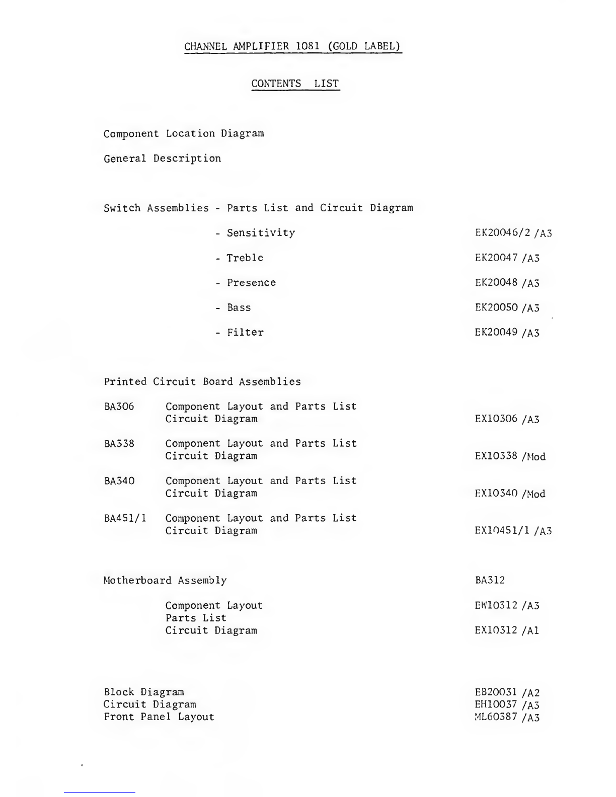
CHANNEL AMPLIFIER 1081 (GOLD LABEL)
CONTENTS LIST
Component Location Diagram
General Description
Switch Assemblies -Parts List and Circuit Diagram
-Sensitivity
-Treble
-Presence
-Bass
-Filter
EK20046/2 /A3
EK20047 /A3
EK20048 /A3
EK20050 /A3
EK20049 /A3
Printed Circuit Board Assemblies
BA306 Component Layout and Parts List
Circuit Diagram
BA338 Component Layout and Parts List
Circuit Diagram
BA340 Component Layout and Parts List
Circuit Diagram
BA451/1 Component Layout and Parts List
Circuit Diagram
EX10306 /A3
EX10338 /Mod
EX10340 /Mod
EX10451/1 /A3
Motherboard Assembly BA312
Component Layout
Parts List
Circuit Diagram
EW10312 /A3
EX10312 /A1
Block Diagram
Circuit Diagram
Front Panel Layout
EB20031 /A2
EH10037 /a3
ML60387 /A3

ML
60387

CHATJNEL Af^PLIFIER 1081
(GOLD LABEL)
The Gold Label on the rear of the module indicates that certain
customer modification have been carried out, making this module
non-interchangeable with other NEVE type 1081 Channel Amplifiers.

CHANNEL AMPLIFIER 1081
SEKSnn/fTY
svy.
PE4K/SMELF
SvJiTtW
-TREtl-E. 'rP.fO I, -n
UPPE* PPE^.’
!
FPE<3SSl- ,
iGrtny.cz— I
j
wa
Ce.hv >
c
•+IQ €•^»^
lower PE ^4
<U- ?*
•-
EAt5 Pf^r/
Sk€LP ^W..
set.S.&TCiT^- c
Cot co.yT<i»L.
H.p/L>»
-iLtcR erf
(R^ Vk'i
EQ. SOL^-^ ~
fR'i (1-] ^
r_j 1
MIC
r? iM?oT
1
tig. 1
^ide vii&v d/ Chajinel amplifier Z03J. showihg the location of siwi itches
artrf- »ai.rt .Ctffflponsnta'. for details of the srnsllef motherbdatfd cc<?sx7iif!iits
sefe fig.. 2.'
Details of the switches are shown
-.%.;.^
Drawing *Vo
.
£7:?C>d46
Eiaoo4i
EK20048
WQQ4^ ,
EK2005O
separately on. the following drawings
.
**
Covxponent
Sehsitxvitg SiHtch.
frdble Swi tch Hs'setib 1y
.
Presence 'Switdh (upper
and lower frequencies)
.
Filter Si/itch Asseirhlg
.
Bass Switch Asscmblg..'
DrV'fiftg EH10 ,037 shows the mptherboatdEA3jL2 as ablock with contact
n\^jers and related wire colour codes for idhhfifit^atioh The' lettered,
sgdkets relate to the module rear connector, r
Individual amplifiers are separately desttibed.
1

CHANNEL AMPLIFIER CONTROLS AND GENERAL COMPONENT LAYOUT
Controls
All controls requiring adjustment during preliminary setting up or the
normal operation of the equipment are on the front panel of the unit.
Two preset controls are mounted on the rear panel and their functions
are as follows:
1) HI/LO Microphone Input
This is asmall toggle switch which selects either high or
.low level impedance at the primary of microphone input
transformer Tl. The line input at T2 is taken directly to
the sensitivity switch via the yellow and grey wires.
?) Fader Preset Equalisation
The small preset potentiometer in series with the equalisation
iN/OUT switch enables compensation to be inserted to allow for
small resistive variations between channel faders.
The sensitivity switch shown in detail on drawing EK20046 has 23
positions. Of these, positions 1to 9are wired to vary the attenuation
required for high level inputs, the attenuation being varied from -20 dB
to +15 dB in 5dB steps. The transition point between the high level and
the low level attenuation occurs between switch positions 8and 9the
difference being 25 dB from +15 dB to -10 dB. The low level attenuation
is switchable in 5dB steps from -5 dB to -80 dB. For details, see
drawing JCK20046.
3) Treble Switch Assembly EK20047
This is adual concentric control comprising asix position switch
selecting the high frequency roll-off points at 3.3 kHz, 4.7 kHz,
6.8 kHz and 15 kHz, the sixth position being an OFF position.
The lOK potentiometer varies the high frequency response above
or below the normal position. Mounted on the front panel
immediately above the switch potentiometer control is apush-
button switch which introduces apeak as an alternative to the
normal shelf characteristic (boost condition only).
Upper/Lower Presence Switch Assemblies
Separate switch/potentiometer controls are employed, each having
an associated Hi Qswitch, the latter being mounted between the
two controls on the front panel. The effect of the Hi Qswitch
when operated is to increase the resistive damping of the tuned
circuit at the presence frequency selected, thereby, substituting
aless acute rise and fall to the boost characteristic. As a
general rule the use of alow Qresponse at the presence boost
frequency is preferred on orchestral music, the high Qbeing
reserved for other types of popular music.
As the upper and lower presence circuits are similar, asingle
circuit diagram is used with the appropriate resistor values
shown
.
Iss. 13.

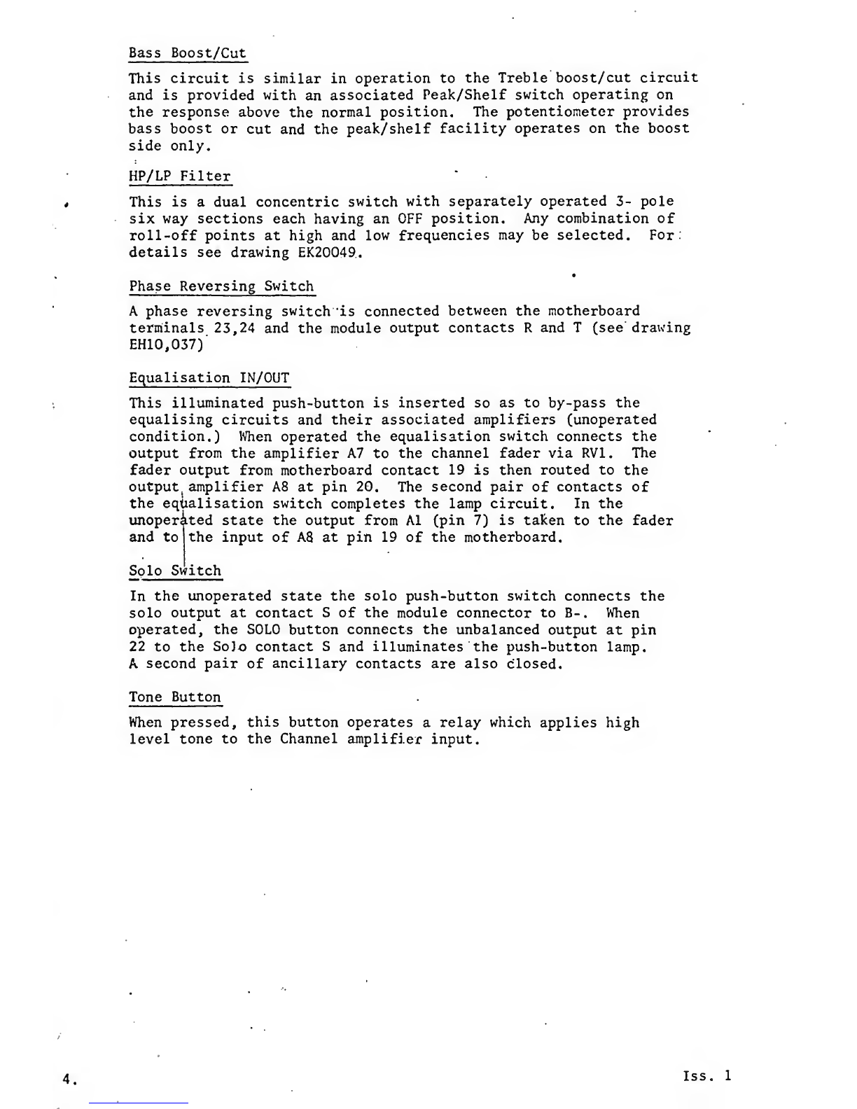
Bass Boost/Cut
This circuit is similar in operation to the Treble boost/cut circuit
and is provided with an associated Peak/Shelf switch operating on
the response above the normal position. The potentiometer provides
bass boost or cut and the peak/shelf facility operates on the boost
side only.
HP/LP Filter
This is adual concentric switch with separately operated 3- pole
six way sections each having an OFF position. Any combination of
roll-off points at high and low frequencies may be selected. For
details see drawing EK20049.
Phase Reversing Switch
Aphase reversing switch ’is connected between the motherboard
terminals 23,24 and the module output contacts Rand T(see drawing
EH10,037)
Equalisation IN/OUT
This illuminated push-button is inserted so as to by-pass the
equalising circuits and their associated amplifiers (unoperated
condition.) When operated the equalisation switch connects the
output from the amplifier A7 to the channel fader via RVl. The
fader output from motherboard contact 19 is then routed to the
output amplifier A8 at pin 20. The second pair of contacts of
the equalisation switch completes the lamp circuit. In the
unoperkted state the output from A1 (pin 7) is taken to the fader
and to the input of A8 at pin 19 of the motherboard.
Solo Switch
In the unoperated state the solo push-button switch connects the
solo output at contact Sof the module connector to B-. When
operated, the SOLO button connects the unbalanced output at pin
22 to the SoJo contact Sand illuminates the push-button lamp.
Asecond pair of ancillary contacts are also closed.
Tone Button
When pressed, this button operates arelay which applies high
level tone to the Channel amplifier input.
4. Iss. 1

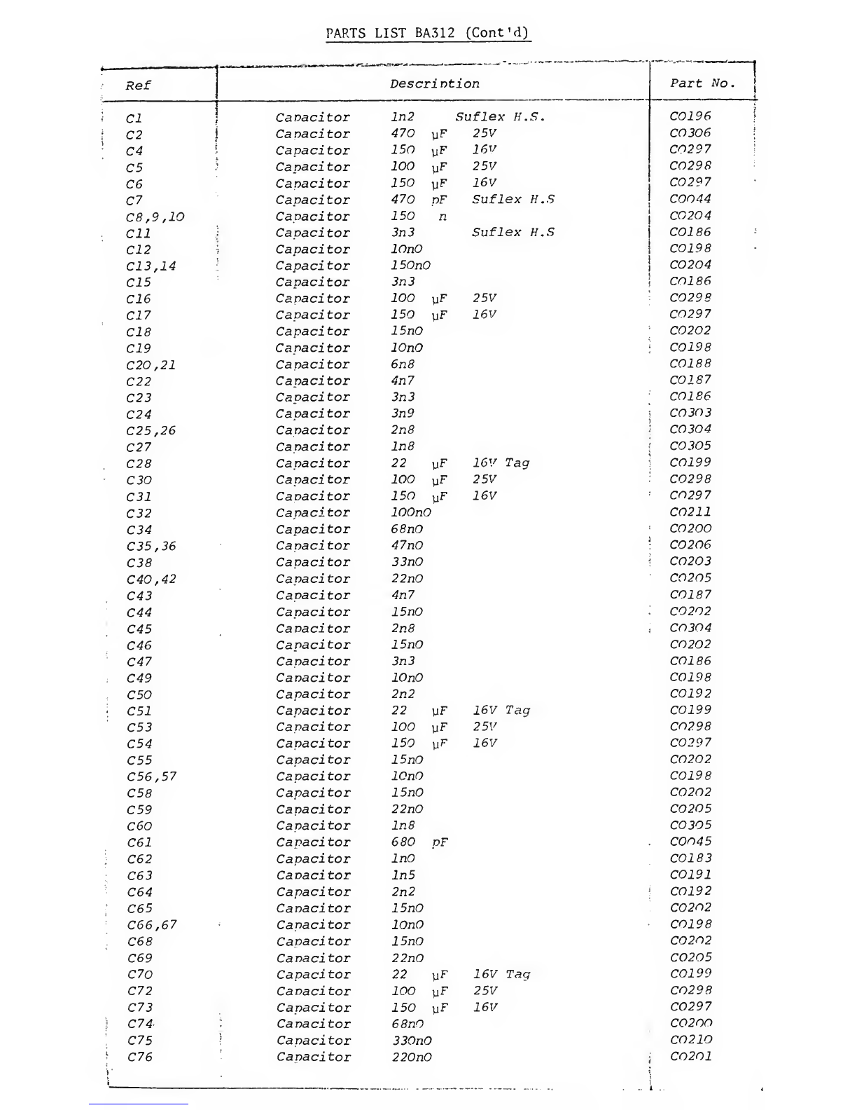
PARTS LIST BA3I2
(USED ON 1081 GOLD LABEL, A32I5 ONLY)
JRef Description iPart No.
Rl Resistor 680 TR4 ±2% R4 680
R3 Resistor 1K5 rr rr R4 1K5
R4 Resistor 47 »' t* R4 47 j
R6 Resistor IKl nnR4 IKl I
R7 Resistor 2KO It n
;R4 2KO 1
!R8 Resistor 2K7 UII R4 2K7 :
iR9 Resistor 7K5 II II R4 7K5
1RIO Resistor 470 II II R4 470
jRll Resistor 47 It II R4 47
iR12 Resistor 4K3 II It R4 4K3
IR13 Resistor 620 II It P4 620
iR14 Resistor lOK II II R4 lOK
R15 Resistor 30K ti II R4 30K
R16-24 Resistor 4M7 Tyne 15 T15 4M7
iR25 Resistor 1K5 TR4 ±2% R4 1K5
R26 Resistor 2K7 II II R4 2K7
.R27 Resistor 47 It II R4 47
:R28 Resistor lOK II II R4 lOK
1R29 Resistor 30K It II P4 30
K
iR30-38 Resistor 4M7 Tyne 15 T15 4M7
:R39 Resistor 1K8 TR4 ±2% P4 1K8
:R40 Resistor 47 It It R4 47
1R41 Resistor lOK II II R4 lOK
R42 Resistor 620 !• It R4 620
R43 Resistor 15K It II R4 15K
R44-57 Resistor 4M7 Tyne 15 T15 4M7
R58 Resistor 620 TR4 ±2% R4 620
R59 Resistor 47 II II R4 47
R60 Resistor lOK If It P4 lOK
R61 Resistor 620 II It R4 620
R62 Resistor 15K It II R4 15K
R63-66 Resistor 4M7 Tyne 15 T15.4M7
R68-75 Resistor 4M7 II II T15 4M7
R76 Resistor 47 TR4 ±2% R4 47
R77 Resistor 620 II II P4 620
R78 Resistor 2KO II II R4 2KO
R79 Resistor 3K9 II II R4 3K9
R80 Resistor 15K It II R4 15K
R82,83 Resistor 100 It II R4 100
R84 Resistor IK8II II R4 1K8
R85,86 Resistor 2K0 It II R4 2K0
R87 Resistor 2K4 II II R4 2K4
R88 Resistor 3K6 II II R4 3K6
R89 Resistor 3K6 II II R4 3K6
R91 Resistor 10 II II R4 10
R92 Resistor 820 II II R4 820
R93
.
1
Resistor 15K II II R4 15K

PARTS LIST BA512 (Cont'd)
•Ref Descrintion Part No
.
1
4
.
;cl Canacitor ln2 Suflex H.S. C0196 i
iC2 Ca nacitor 470 yF 2SV CO306 i
C4 Capacitor ISO yF 16V C0297 i
C5 Capaci tor 100 yF 2SV C0298
C6 Cavacitor ISO yF 16V C0297
C7 Capacitor 470 pF Suflex H.S C0044
C8 ,9 ,10 Caoaci tor ISO nCO204
Cll Capacitor 3n3 Suflex H.S COl 86
C12 Capaci tor lOnO CO19 8
C13,14 Capacitor ISOnO C0204
CIS Capaci tor 3n3 C0186
C16 Capacitor 100 yF 2SV C029S
C17 Capacitor ISO yF 16V C0297
C18 Capaci tor ISnO C0202
C19 Capacitor lOnO CO19 8
C20,21 Capacitor 6n8 C0188
C22 Capacitor 4n7 CO187
C23 Capacitor 3n3 COl 86
C24 Capacitor 3n9 CO303
C25,26 Capacitor 2n8 CO304
C27 Capacitor ln8 C030S
C28 Capacitor 22 yF 16V Tag CO19 9
C30 Capacitor 100 yF 2SV C0298
C31 Capaci tor ISO yF 16V C0297
C32 Capacitor lOOnO C0211
C34 Capacitor 68n0 C0200
C35,36 Capacitor 47nO C0206
C38 Capacitor 33nO C0203
C40,42 Capacitor 22nO C020S
C43 Capacitor 4n7 COl 87
C44 Capacitor ISnO C0202
C45 Capacitor 2n8 C0304
C46 Capaci tor ISnO C0202
C47 Capaci tor 3n3 COl 86
C49 Capacitor lOnO CO19 8
,C50 Capacitor 2n2 CO192
•C51 Capacitor 22 yF 16V Tag CO199
C53 Capacitor 100 yF 2SV C02.98
C54 Capaci tor ISO yF 16V C0297
CSS Capacitor ISnO C0202
CS6,S7 Capacitor lOnO CO19 8
CS8 Capacitor ISnO C0202
CS9 Capacitor 22nO C020S
C60 Capacitor ln8 C030S
C61 Capacitor 680 pF C0O4S
.C62 Capacitor InO COl 83
C63 Ca pad tor InS C0191
C64 Capacitor 2n2 CO192
;C65 Capacitor ISnO C02O2
C66,67 Capacitor lOnO CO19 8
C68 Capaci tor ISnO C0202
C69 Capacitor 22nO C020S
C70 Capaci tor 22 yF 16V Tag CO19 9
C72 Ca pad tor 100 yF 2SV C0298
C73 Capacitor ISO yF 16V C0297
iC74 Capacitor 68nO C020O
'C7S ?Capacitor 330n0 C0210
‘C76 Capacitor 220n0 C0201
r
I

PARTS LIST BA312 (Cont'd)
Ref Descrintion
C77 iCapacitor lOOn
C78 11Capacitor 47n
C79 \1Capacitor lOnO
C80 !
'Capaci tor 1.5 yF
C81 1
1Capacitor 680n
CS2 ]Canacitor 470n0
C83 ;[Capacitor 220n0
C84,85 Capacitor 330n0
C86 1ICanacitor 220nO
C87 'Canacitor lOOnO
C88 Canacitor 47nO
C89 Canacitor lOnO
C90 Capacitor 68nO
C91 Capacitor 22 yF 16V Tag
C93 Canacitor 100 yF 25V
C94,95 Canacitor 150 yF 16V
C96 Canacitor 470 yF 16V
C98,99 iCanacitor 100 yF 25V
CIOQ \
1Capaci tor 22 yF 16V Tag
ClOl \Canacitor 22 yF 16V Tag
C102 Capacitor 470 yF 25V
C103 Capacitor 100 nF Suflex H.S
C105 \
1Canacitor 1000 yF 25V
C106 Capaci tor 180 nF Suflex H.S
T1 Input transformer 10468
T2 Innut transformer 31267
D1 Zener Diode ZF 8.2V
L2 Inductor VT22675
L3 Inductor VT22674
Qty 45 Cambion sockets
Qty 102 Cambion Pins
Printed Circuit Board (unassembled)
Part No
C0211
C0206
C0198
IC0265
\C0208
;C0209
IC0201
C0210
IC0201
IC0211
’C02O6
C0198
C02OO
CO199
C0298
iC0297
C0306
C0298
CO199
CO19 9
CO380
C0039
C0333
C0040
T0004
T0006
XXI 1507
T0098
T0O97
C0240
C0258
B312


TITLE |/| ETC? F-v_oT=^ P.C.S. roR
Pupef» Nevp ACompriny ltd »*'wn lh»- ropyrtqhl of th»<>
1».jvv«ntj wvhj/ Hoot fo bP Lopiofi oi f1»sr.u*serl
np.ifl oi vvboip to-» lbif(1 prirly wthn^M p(» m*ss i* »fj
ITEM
No.
NEL
PART N°.
MA/vJoF^A(C'~T"0
to IO-4 I
^\y 104- E>\
ETW 104 S.I
104-til /|
DESCRIPTION
II
PART LIST No. pi^ 104S^ 1/\
SHT. IOF 2.
FIRST USED ON A3215
A4
A4
OOiM
e. 4-^1
OO
CO i
C02BB
DRAWN C>. dooltsiSoN
CHFCKF
PART LIST N- Pl_ ic:>4
SHT 1u.
O

N.E.L.
PART No.
e-4 4“7K
(Z4 4K.7
R.4 2KO
DESCRIPTION
-jS% 3oo o«4ks
—_K_ -n— 4“7K —
—
——aKO .—^^7 .a.
drawn: b. <2o&jnscai
checked:
ADME17457A
PART LIST No. f=>ulOAS\/l
SHT. "7 OF 2
Rupert Neve &Comparty Ltd.

PRINTED CIRCUIT BOARD ASSEMBLY BA45 I/
I
EQ RELAY/FLIP FLOP
COMPONENT LAYOUT
R6 0R5 R7
-- ^/7 //
C2^C30 O
V 9 '9
Cl TR 1
o
R3 O
R4I
R1 1Z71~
R20
TR2 08,
o09
:
Z1 07
on
ow
PARTS LIST
Ref Descri ntion
:
Ri iResistor 2X2 TR4 5%
R2 iResistor 300
!^-3 iResistor 47X0
!R4 iResistor 47X0
!R5 ;Resistor 4X7
iR6 iResistor 4X7
:R7 Resistor 2X0
R8 Resistor 2X0
Cl Ca naci tor lO nPolycarbonate
C2 Ca naci tor 22 16V TAG
C3 Canaci tor 22 yF 16V TAG
Di ode BAX16
'TRl Transistor BC184 XC
.TR2 Transistor BC184 XC
Transistor Mounting Pad (for T0043)
Transistor Mounting Pad (for XX12808)
Relay Teledyne 712m-26
Printed Circuit Board (unassembled)
Part Mo.
R4 2K2
R4 300
R4 47KO
P.4 47X0
P4 4X7
Rd 4X7
!R4 2X0
R4 2X0
C0321
CO19 9
CO19 9
TOO41
TOO43
T0043
T0O59
T0077
XX1280
8
B451

DRAWING
N? EX 10306
INPUT B3
3C 2KKC
THIS SECTION NOT USED ON BA305/H
CJT PUT A
INPUT A
1
1
tri „.Cl
'bC214KC “7-5p
rp
OUTPU'
BC2U«C
5/6/73!23-1172i 30-10-72
10714 10564
FIRST USED ON
ISSUE
DATE DRN.
CHANGE "LMC
NOTE N9 I^HECKED
FINISH
TITLE
BA306
LINrAFx IANGUlAPJ HOLFS !
I- jC'' (
I-TO"
CHECKED
DUAL VOLI-<OH FOLLOWER
.Company tx 1030
1972

I
^£Tu.'Pi^M C'2lL£cyc^(l 4
£K\\TreQ T£m-
J


3G/1/73 c30/4/73 c3/8/
7
3
10f^41 •^1069S 10743
^Tfie Neve Group of Companies
TITLE BA338 PLUG IN AMR
This drawing is the property of this company ti
may not be reproduced or disclosed to athird
party without the permission of this company.
3Q'n 10525 DATE
DRAWING
NUMBER EX10338

NM7827
Other manuals for 1081
1
Other AMS Neve Amplifier manuals