B&K 415 User manual

/BftfModel 415
.--------·-,-~-·----, _j
Sweep/MarkerGener tor
A Product of DYNASCAN CORPORATION 1801 West Belle Plaine • Chicago, Illinois 130613 _ ,.....,...
PRICE $5.00

t
INSTRUCTIONMANUAL
FOR
MODEL415
SWEEP/ MARKERGENERATOR
8 & K DIVISION OF DYNASCAN CORPORATION
1801 W. Belle Plaine Avenue
Chicago, Illinois 60613
Copyright 1972

t
)
INTRODUCTION
The objectives of the Model 415 Sweeo Marker
Generator and this manual cue as follows:
A. To simplify the sweep alignment of cxlltelev1sion
receivers, particularly color sets. S1mplificction
is accomplished by an instrument design which
concentrates all the required alignment tools
exclusive of oscilloscope and VTVM) into a
single versatile package. Functional grouping
of all controls and features adds to efficiency
ond ease of operation.
B. To enable you to proceed confidently through
complete alignment procedures in minimum
time. The importance of confidence in ihe test
equipment and alignment procedures cannot be
overemphasized.
C. To provide speed of alignment and alignment
verification which are essential in attaining effi-
cient and profitable operations. The 415 is de-
signed to put sweep alignment and alignment
verification into the proper perspective with
regard to overall television servicing by elim-
inating complexity and drastically reducing the
time required for these functions.
D. To provide an instrument which will not be ob-
soleted by future television receiver designs.
The Model 4 !5 is the result of an extensive sur-
vey of older receivers and those currentlv on
the market as well as a projection of future.tele-
vision receiver designs.
Without the Model 415 numerous separate pieces
of equipment have to be grouped together in
order to begin sweep alignment. These include
a sweep generator capable of furnishing video
sweep, i-f sweep and r-f sweep. Usually more
than one generator is required. A second re-
quirement is a marker generator capable of
furnishing reference markers in the video, i-f and
r-f ranges. Without the 415, this again usually
requires more than one generator. If this gen-
erator is tunable, it can furnish only one refer-
ence marker at a time. Also, the fact that the
generator is tunable raises questions of calibra-
tion accuracy. A marker adder is also used,
particularly in chroma circuit alignment. Sep-
arate bias supplies are also required. Some
alignment procedures call for simultaneous ap-
plication of up to three bias voltages. In many
procedures a demodulator is required to view
r-f, i-f, or chroma envelopes. An oscilloscope
and voltmeter complete the equipment require-
ments.
After the set-up is complete and alignment is
under way the technician usually finds that the
amplitude and tilt of the observed waveforms
are affected by ti1c of the interconnect
ing wues end cab.es 111 Li'3 set-up crnd that
can uiso ~)0 vaned touchmg foe leuds, cu;1lc,,
cmc.l equipment. compietion -::ifthe
r,1ent procedure the techntcicm cannot r1elp
·sonder if the response curves which he t1W)
lir1oll y obtained ure those of the :,,
ce1ver itself or me oartlv affected his uliqn-
ment set-up. " " · ,
The Model 41'.i has been designed to eliminate
tl'.e problems, normolly encountered in sweep
c11gnment. This totally solid-state unit is cooa
ble of providing i-f sweep, r-f sweep on telt~v,
sion Channels 4 and 10, video sweep, 10.':' J\1Hz
i-f sweep for f-m receivers and crystal-controlleo
post injection markers for accurate frequency
identification on ull sweep ranges. In additio:;
crystal-controlled output frequencies are ovoii-
ab!e for spot olignment of '.:ap circuits and
bandpass circuits.
Three self-contained crdjustable bias supplies of
reversible polarity are more than odequate for
all alignment tasks. The signal cable is properly
terminated to minimize alignment errors crnd
"hot" leads coused by standing waves. All ac-
cessories are provided: r-f demodulator probe,
a direct cable with built-in isolating resistor, an
r-f cable with built-in terminations which can be
selected by a switch, 1-f load blocks, ond bias
leads. Only un oscilloscope and a VTVM are
required to complete the alignment set-up.
Additional features include unity gain through
the signal-processing circuits of the 415 so that
peak-to-peak amplitudes can be monitored con-
tinuously during crlignments; a 15,750 Hz filter
which enables the user to perform sweep align-
ment without disabling the horizontal output cir-
cuits; built-in low-frequency compensation to
eliminate pattern tilt errors resulting from use of
an oscilloscope with poor low-frequency re-
sponse; marker tilt capability: the markers can
be switched from vertical to horizontal positions.
Alignment procedures are streamlined by the
versatility and functional design of this
instrument.
This manual will familiarize you with the appli-
cations and features of the 415, as well as the
internal circuit functions of the instrument itself.
In addition the signal processing circuits of color
and black and white television receivers will be
reviewed and the importance of proper align-
ment emphasized. In this way you can proceed
rapidly and confidently through alignment pro-
cedures with a complete understanding of how
and why the 415 signals are generated and how
the television receiver responds to them.
3
TABLEOFCONTENTS
Page
INTRODUCTION . . . . . . . . . . . . . . . . . . . . . . . . . . . . . . . . . . . . . . . . . 3
LIST OF ILLUSTRATIONS . . . . . . . . . . . . . . . . . . . . . . . . . . . . . . . . . 5
SPECIFICATIONS . . . . . . . . . . . . . . . . . . . . . . . . . . . . . . . . . . . . . . . . 7
TELEVISION SIGNALS AND RECEIVER FUNCTIONS
2.0 TELEVISION SIGNAL PROCESSING . . . . . . . . . . . . . . . . . 10
2.1 THE TRANSMITTED TELEVISION SIGNAL . . . . . . . . . . . 10
2.2 THE TELEVISION RECEIVER . . . . . . . . . . . . . . . . . . . . . . . 14
2.2.1 TYPICAL TELEVISION RECEIVER BLOCK
DIAGRAMS . . . . . . . . . . . . . . . . . . . . . . . . . . . . . . . . . 14
2.2.2 TELEVISION RECEIVER TUNED CIRCUITS . . . . 16
2.2.2.1 STAGGER-TUNED CIRCUITS ........... 16
2.2.2.2 TRAP FREQUENCY CIRCUITS . . . . . . . . . 16
2.2.2.3 USE OF OVERCOUPLING IN
TUNED CIRCUITS . . . . . . . . . . . . . . . . . . . . . 17
2.2.2.4 IMPORTANCE OF TUNING SLUG
LOCATION IN TUNED CIRCUITS ....... 17
2.3 SWEEP ALIGNMENT . . . . . . . . . . . . . . . . . . . . . . . . . . . . . . . 18
2.3.1 IMPORTANCE OF SWEEP ALIGNMENT ........ 18
2.3.2 SWEEP ALIGNMENT METHODS . . . . . . . . . . . . . . . 20
FUNCTIONAL DESCRIPTION OF THE MODEL 415 CIRCUITS
3.0 MODEL 415 SWEEP/MARKER GENERATOR
BLOCK DIAGRAM ................................. 23
3.1 SWEEP CIRCUITS . . . . . . . . . . . . . . . . . . . . . . . . . . . . . . . . . 23
3.2 44 MHz SWEEP OSCILLATOR AND
1-F MARKER SYSTEM . . . . . . . . . . . . . . . . . . . . . . . . . . . . . . 23
3.2.l 44 MHz SWEEP OSCILLATOR ................ 23
3.2.2 1-F MARKER OSCILLATORS .................. 23
3.2.3 EXTERNAL MARKER INPUT . . . . . . . . . . . . . . . . . . 23
3.2.4 100 KHz MARKERS .......................... 23
3.3 MARKER DETECTOR AND AMPLIFIERS . . . . . . . . . . . . 23
3.4 PATTERN AMPLIFIERS ............................. 24
3.5 PIX OSCILLATOR AND CHROMA FUNCTION 25
3.6 CHANNEL 4 AND CHANNEL 10 MIXING
OSCILLATORS Q301 AND Q303 .................... 25
3.7 VIDEO SWEEP AMPLIFIER Q401 ..•............... 26
3.8 MARKER FREQUENCY RELATIONSHIPS ............ 26
3.9 10.7 MHz CIRCUJTRY ............................. 27
3.10 POWER SUPPLIES AND BIAS SUPPLIES ............ 27
INTRODUCTION TO TELEVISION ALIGNMENT USING
THE MODEL 415
4.0 MATCHING THE MODEL 415 TO THE RECEIVER .... 28
4.1 GENERAL ALIGNMENT INFORMATION ............ 28
4.1.1 VIDEO SWEEP ALIGNMENT OF
CHROMA CIRCUITS . . . . . . . . . . . . . . . . . . . . . . . . . . 28
4.1.2 1-F AND CHROMA ALIGNMENT CHECKS . . 28
4.1.3 PREALIGNMENT OF TRAPS AND TUNED
CIRCUITS USING MARKER FREQUENCIES . . . . . 28
4.1.4 OVERALL RECEIVER ALIGNMENT CHECK .... 28
4.2.1 VIDEO ...................................... 28
4.2.2 IF POSITION ................................ 30
4.2.3 MKR ........................................ 32
4.2.4 MOD MKR . . . . . . . . . . . . . . . . . . . . . . . . . . . . . . . . . . 35
4.2.5 CHANNEL 4 . . . . . . . . . . . . . . . . . . . . . . . . . . . . . . . . . . 37
4.2.6 CHANNEL 10 . . . . . . . . . . . . . . . . . . . . . . . . . . . . . . . . 38
4.2.7 10.7 MHz .................................... 39
OPERATING PROCEDURES
4
5.0 USING THE MODEL 415 SWEEP/MARKER
GENERATOR ...................................... 41
5.1 CONTROLS AND OUTPUTS ......................... 41
5.2 EQUIPMENT INTERCONNECTION AND
SET-UP PROCEDURE .............................. 43
5.3 USE OF MODEL 415 CONTROLS ................... 44
5.4 COMPENSATION FOR POOR LOW FREQUENCY
RESPONSE OF THE OSCILLOSCOPE . . . . . . . . . . . . . . . . 46
5.5 USE OF 100 MHz MARKERS IN
TELEVISION ALIGNMENT .......................... 47
5.6 USING THE CUSTOMER OPTION OSCILLATOR ...... 47
5.6.2 USING THE SPARE MARKER OSCILLATOR AS
A VARIABLE FREQUENCY SOURCE ................. 47
6.0 TELEVISION RECEIVER ALIGNMENT USING
THE MODEL 415 .................................. 48
6.1 SIMPLIFIED PROCEDURE FOR DIAGNOSING
NEED FOR ALIGNMENT ........................... 48
6.2 ANALYZING THE RESPONSE CURVES . . . . . . . . . . . . . . 50
6.3 GENERAL ALIGNMENT INFORMATION ............ 52
6.3.1 LOCALIZING ALIGNMENT PROBLEMS ........ 52
6.3.2 ALIGNMENT METHODS . . . . . . . . . . . . . . . . . . . . . . 53
6.3.2.1 TUNER LINK ......................•... 53
6.3.3.2 I-F ALIGNMENT . . . . . . . . . . . . . . . . . . . . . . 54
6.3.2.3 CHROMA ALIGNMENT . . . . . . . . . . . . . . . . 54
6.3.2.4 RECORDING ALIGNMENT REFERENCE
INFORMATION ....................... 54
7.0 ALIGNMENT TOUCH-UP PROCEDURES ............. 55
7.1 PRELIMINARY ..................................... 55
Page
7.2 TRAP ADJUSTMENTS .............................. 55
7.3 I-F RESPONSE, TILT ADJUSTMENT.
MIXER INJECTION . . . . . . . . . . . . . . . . . . . . . . . . . . . . . . . . 56
7.4 CHROMA CIRCUIT ADJUSTMENT ................... 56
7.5 TILT ADJUSTMENTS, ANTENNA INJECTION . . . . . . . . 56
8.0 COMPLETE 1-F AND CHROMA ALIGNMENT
PROCEDURE USING THE MODEL 415 .............. 58
8.1 TRAP ALIGNMENT USING MODULATED MARKERS .. 58
8.2 PRE-ALIGNMENT OF I-F BANDPASS COILS AND
TRANSFORMERS (When Specified) . . . . . . . . . . . . . . . . . . 58
8.3 TUNER LINK ALIGNMENT (When Specified) . . . . . . . . 58
8.4 SWEEP ALIGNMENT OF THE 1-F STAGES USING
THE MODEL 415 .................................. 59
8.5 CHROMA CIRCUIT ALIGNMENT ................... 61
8.5.2 BANDPASS AMPLIFIER ALIGNMENT USING
DIRECT VIDEO SWEEP ....................... 61
8.5.3 CHROMA ALIGNMENT USING SIGNAL
INJECTION AT THE ANTENNA TERMINALS OF
THE RECEIVER OR AT THE MIXER TEST
POINTS ..................................... 61
9.0 ADDITIONAL TELEVISION ALIGNMENT PROCEDURES
USING THE MODEL 415 ........................... 63
9.1 TV SOUND ALIGNMENT .......................... 63
9.1.l USING THE MODEL 415 IN TELEVISION
SOUND ALIGNMENT . . . . . . . . . . . . . . . . . . . . . . . . 63
9.2 AUTOMATIC FINE TUNING (AFT) .................. 64
9.2.1 OPERATION OF AFT CIRCUITS .............. 64
9.2.2 ALIGNMENT OF AFT CIRCUITS . . . . . . . . . . . . . . 66
9.3 CONDENSED WORK GUIDE ........................ 67
MANUFACTURERS' ALIGNMENT PROCEDURES USING
THE MODEL 415
10.0 INTRODUCTION ................................... 69
10.l ALIGNMENT OF MAGNAVOX MODEL T933 ........ 69
10.2 ALIGNMENT OF THE PHILCO-FORD "S" LINE
COLOR TELEVISION RECEIVER . . . . . . . . . 73
11.0 OTHER USES OF THE MODEL 415 .................. 78
11.l ALIGNMENT OF FM RECEIVERS USING THE
MODEL 415 ....................................... 78
11.1.1 10.7 MHz 1-F ALIGNMENT .................. 78
11.1.2 CHECKING FM RECEIVER TRACKING ...... 79
11.2 VARIABLE FREQUENCY GENERATOR CALIBRATION 81
11.2.7 USING HARMONIC RELATIONSHIP
TO CALIBRATE VARIABLE FREQUENCY
GENERATORS .............................. 82
11.3 AM BROADCAST RECEIVER TUNING AND
TRACKING CHECKS . . . . . . . . . . . . . . . . . . . . . . . . . . . . . . . 82
11.4 ADDITIONAL USES OF THE MODEL 415 ............ 82
MODEL 415 ADJUSTMENTS AND MAINTENANCE
12.0 MAINTENANCE AND ADJUSTMENT PROCEDURES .. 83
12.1 TROUBLESHOOTING INFORMATION AND
PROCEDURES . . . . . . . . . . . . . . . . . . . . . . . . . . . . . . . . . . . . . 83
12.1.1 INTERCONNECTING CABLES, TEST LEADS
AND SWITCHES . . . . . . . . . . . . . . . . . . . . . . . . . . . . . 83
12.1.2 REGULATED POWER SUPPLIES AND BIAS
SUPPLIES . . . . . . . . . . . . . . . . . . . . . . . . . . . . . . . . . . 83
12.1.3 HORIZONTAL SWEEP CIRCUITS ............. 84
12.1.4 PATTERN AMPLIFIER CIRCUITS
(Ql9 and Q20) .............................. 84
12.1.5 MARKER DETECTORS AND AMPLIFIERS ..... 85
12.1.6 VIDEO IF/RF ATTENUATOR Q306 ........... 85
12.2 USE OF MAINTENANCE INFORMATION IN
TROUBLESHOOTING . . . . . . . . . . . . . . . . . . . . . . . . . . . . . . 85
12.3 REPLACEMENT OF DEFECTIVE COMPONENTS . . . . . . 85
12.4 INTERNAL ADJUSTMENT PROCEDURES ............ 86
12.4.1 MARKER OSCILLATOR ADJUSTMENTS ....... 86
12.4.2 CHANNEL 4 OSCILLATOR ADJUSTMENT ..... 86
12.4.3 CHANNEL 10 OSCILLATOR ADJUSTMENT ... 86
12.4.4 PIX OSCILLATOR ADJUSTMENT (Bottom Cover
of Model 415 Removed) ...................... 86
12.4.5 USING THE SPARE MKR OSCILLATOR ....... 86
12.4.5.1 USING THE SPARE MKR OSCILLATOR
AS A CRYSTAL-CONTROLLED MARKER
OSCILLATOR ....................... 87
12.4.5.2 USING THE SPARE MARKER AS A
VARIABLE FREQUENCY SOURCE . . . . 87
12.4.5.3 CALIBRATION OF THE SPARE MKR
OSCILLATOR FOR VARIABLE
FREQUENCY OPERATION ........... 88
12.4.6 BALANCING SWEEP OUTPUTS OF HORIZONTA,L
SWEEP AMPLIFIER Ql4 ..................... 88
12.4.7 ADJUSTMENT OF SWEEP OSCILLATOR
VARACTOR BIAS . . . . . . . . . . . . . . . . . . . . . . . . . . . 88
12.4.8 SWEEP LINEARITY ADJUSTMENT . . . . . . . . . . . . 88
)
LIST OF ILLUSTRATIONS
Section 1.0 415 SWEEP/MARKER GENERATOR
SPECIFICATIONS
Fig. 1.1 Accessories Furnished With the Model
415.
Section 2.0 TELEVISION SIGNAL PROCESSING
Fig. 2.1 Simplified Television Signal Spectrum
(Channel 10).
TABLE 2.1 TELEVISION CHANNEL FREQUENCY
SPECTRUM
Fig. 2.2 Frequency Spectrums of Channels 9, 10,
and 11 Showing Relationships of Adja-
cent Channel Interfering Carriers.
Fig. 2.3 Block Diagram of Typical Black and
White Television Receiver.
2.4 Block Diagram of Typical Color
Television Receiver.
Fig. 2.5 Simplified Television Receiver Block
Diagram.
Fig. 2.6 Signal Processing Circuits of Color
Television Receiver.
Fig. 2.7 Typical Tuner and I-F Response Curves
Showing Relative Bandwidths.
Fig. 2.8 Overall Response of Stagger-Tuned
Circuits.
Fig. 2.9 Effects of Trap Circuits on Overall
Curves.
Fig. 2.10 Effects of Coupling on Overall Response
of Two Tuned Circuits.
Fig. 2.11 Core Positions at Resonance in Tunable
Coil Assemblies.
fig. 2.12 Effects of Slug Locations in Double-
Tuned Circuits.
Fig. 2.13
Fig. 2.14
Section 3.0
Fig. 3.l
Fig. 3.2
Fig. 3.3
Typical Chroma Bandpass Transformer.
Television Response Curves Obtained
Using Sweep-Frequency Techniques.
MODEL 415 SWEEP/MARKER
GENERATORBLOCKD1AGR1'.\M
Model 415 Block Diagram.
Video Sweep Generation.
Marker Frequency Relationships in the
Model 415.
Section 4.0 MATCHING THE MODEL 415 TO THE
RECEIVER
Fig. 4.l Model 415 Block Diagram for VIDEO
Function.
Fig. 4.2 Color TV Receiver Block Diagram fo:r
Video Alignment
Fig. 4.3 Chroma ResponsH Curve with Markers
Added.
Fig. 4.4 Model 415 Block Diagram for I-F Align-
ment and Overall Chroma Alignment.
Fig. 4.5 Color TV Receiver Block Diagram for
I-F and Overall Chroma Alignment.
Fig. 4.6 Typical I-F Response Curve with
Reference Markers Added.
Fig. 4.7 Enlarged Portion of I-F Response Curve
Showing Sound and Chroma Region.
Fig. 4.8 Reversal of Sweep of Figure 4.7 by Use
of CHROMA Switch.
Fig. 4.9
Fig. 4.10
Fig. 4.11
Fig. 4.12
Fig. 4.13
Fig. 4.14
Fig. 4.15
Fig. 4.16
4.17
Fig. 4.18
Fig. 4.19
4.20
fig. 4.21
Seeton 5.0
Fig. 5.1
fig. 1.1
Fig. 6.2
Fig. 5.3
Fig. 5.4
Chroma Bandpass Response Curve.
Model 415 Block Diagram for MKR
Function.
Color TV Receiver Block Diaaram for
MKRFunction.
~
Model 415 Block
MKR Function.
Color TV Receiver Block Diagro:m for
MOD MKB Function.
415 Block ;irr,rrn"f-m for CH 4 Function.
Color TV Receiver Block Jirrrrn'fl"Yl for
CH 4 Function.
Setting Fine Tuning Using S01.:.::1dNotch
of Response Curve (Channel 4 Mmker
Frequencies Shown).
Increasing Sound Notch Hesolntion io
Adjust Receiver Fine ControL
415 Block Diagram ior CH 10 Function.
Color TV Recei:11",r Block for
CH 10 Funet.ion ..
Model 415 Block
"~~
•.
~,~
fo:c 10.7 MHz
Function.
Typical f ..M Receiver Block Diugrnm.
USING THE MODEL 415
SWEEP/MARKER GENERATOR
Front Panel Controls and Outputs of the
Model 415.
(Repeated) Accessories Furnished with
the Model 415.
Equipment Interconneciion.
Centering Sweep Hange Use of ADJ
PIX and ADJ SND Markers.
Receiver I-F Response Between ADJ PIX
o:nd ADJ SND Markers.
Fig. 5.5 Ttpical I-f Response Curve with
Markers Added.
Fig. 5.6 Response Curve of Figure 5.5 with
Markers Tilted.
Fig. 5.7 Using Sweep Width Control to Enlarge
Portion of l-F Response Curve.
fig. 5.8 Location of Low Frequency Compensa-
tion Control (R-99).
5.9 Correction of Pattern Tilt Using the
Model 415 Low Frequency Compensa-
tion Control (R-99).
Fig. 5.10 Using 100 KHz Markers With I-F
Reference Markers.
5

Section 6.0 TELEVISION RECEIVERALIGNMENT Section 9.0 ADDITIONALTELEVISION
USING THE MODEL 415 ALIGNMENT PROCEDURES
Fig,. 5.7B (Repeated) Sweep Width Reduced to USING THE MODEL 415
Show Only Sound and Chroma Portion Fig. 9.1 Observing Sound Demodulator
of I-F Response. "S"-Curve.
Fig. 4.16 (Repeated) Setting Fine Tuning Using Fig. 9.2 Typical AFT Circuit.
Sound Notch of Response Curve (Chan- Fig. 9.3 AFT Discriminator "S"-Curve.
nel 4 Marker Frequencies Shown). Fig. 9.4 Using 100 KHz Markers to Determine
Fig. 4.17 (Repeated) Increasing Sound Notch Frequency Separation of Discriminator
Resolution to Adjust Receiver Fine Peaks.
Tuning Control. Fig. 9.5 Condensed Work Guide for Television
Fig. 5.7B (Repeated) Sweep Width Reduced to Alignment Using the Model 415.
Show Only Sound and Chroma Portion
of I-F Response. Section 11.0 OTHER USES OF THE MODEL 415
Fig.6.1 Reversal of Sweep when Chroma Fig. 4.21 (Repeated) Typical F-M Receiver Block
Switch is Turned On.
Fig. 4.9 (Repeated) Chroma Bandpass Response Diagram.
Curve. Fig. 11.1 Typical 10.7 MHz I-F Response Curve
Fig. 6.2 Typical Manufacturer's Response with 100 KHz Markers Added.
Curves with Allowable Variations Fig. 11.2 Typical 10.7 MHz Discriminator
Indicated. Response Curve with 100 KHz Markers
Fig. 6.3 Response Curves Within Limits of Added.
Figure 6.2. Fig. 11.3 Checking F-M Receiver Tracking at the
Fig. 6.4 1-FResponse with Sound Trap Tuned to Low End of the F-M Band.
Fig. 11.4 Checking F-M Receiver Tracking Using
Chroma Frequency. the 9th and 10th Harmonics of the 10.7
Fig. 6.5 Typical Response Curves Showing MHz Sweep.
Effects of Misalignment of Tuned Fig. 11.5 Use of 100 KHz Markers in the Calibra-
Circuits.
Fig. 6.6 Detector Load Blocks Required for tion of Variable Frequency Generators.
Tuner Link Adjustment. Section 12.0 MAINTENANCE
Fig. 6.7 Tuner Link Response Curve with ce
Markers Added. Fig. 12.1 Modification of Spare Marker Oscillator
for Variable Frequency Operation.
Fig. 3.1 (Repeated) Model 415 Block Diagram.
Section 7.0 ALIGNMENTTOUCH-UPPROCEDURES Fig. 4.1 (Repeated) Model 415 Block Diagram for
VIDEO Function.
Fig. 7.1 400 Hz Video Detector Output When Fig. 4.4 (Repeated) Model 415 Block Diagram for
Using Modulated Markers. I-F Alignment and Overall Chroma
Fig. 4.16 (Repeated) Setting Fine Tuning Using Alignment.
Sound Notch of Response Curve Fig. 4.10 (Repeated) Model 415 Block Diagram for
(Channel 4 Marker Frequencies Shown). MKR Function.
Fig. 4.17 (Repeated) Increasing Sound Notch Fig. 4.12 (Repeated) Model 415 Block Diagram for
Resolution to Adjust Receiver Fine MOD MKR Function.
Tuning Control. Fig. 4.14 (Repeated) Model 415 Block Diagram for
CH 4 Function.
Fig. 4.18 (Repeated) Model 415 Block Diagram for
CH 10 Function.
Section 8.0 COMPLETE 1-FAND CHROMA Fig. 4.20 (Repeated) Model 415 Block Diagram for
ALIGNMENT PROCEDURE 10.7 MHz Function.
USING THE MODEL 415 Fig. 12.2 Parts Layout for Marker, Waveform
Fig. 6.7 (Repeated) Tuner Link Response Curve Generator, and Pattern Amplifier Board
with Markers Added. (Viewed from Component Side).
Fig. 4.16 (Repeated) Setting Fine Tuning Using Fig. 12.3 Parts Layout for Power Supply/RF
Sound Notch of Response Curve Board (Viewed from Component Side).
(Channel 4 Marker Frequencies Shown). Fig. 12.4 Parts Layout for Sweep Oscillator
Fig. 4.17 (Repeated) Increasing Sound Notch Board (Viewed from Component Side).
Resolution to Adjust Receiver Fine Fig. 12.5 Parts Layout for Pix Oscillator Board
Tuning Control. (Viewed from Component Side). I
Fig. 5.7B (Repeated) Sweep Width Reduced to Fig. 12.6 Waveform Generator Waveforms. { t
Show Only Sound and Chroma Portion TABLE 12.1 Troubleshooting Chart. \
of I-F Response.
Fig. 6.1 (Repeated) Reversal of Sweep when TABLE 12.2 Model 415 Switching Chart.
Chroma Switch is Turned On. TABLE 12.3 Transistor Voltage Chart.
6

SPECIFICATIONS
1.0 415 SWEEP/MARKER GENERATOR
SPECIFICATIONS
1.1 Outputs available (selected by FUNCTION
switch at single output jack):
a. Video Sweep
b. IF Sweep
c. Markers, unmodulated
d. Modulated markers
e. Channel 4 RF Sweep
f. Channel 10 RF Sweep
g. 10.7 MHz Sweep
1.2 Sweep Width:
a. IF, CH 4, CH 10-less than l MHz to over
10 MHz
b. 10.7MHz-less than 200 KHzto over 2 MHz
c. Video-less than 1 MHz to over 6 MHz
1.3 Sweep Frequency Coverage (Sweep plus
center frequency adjustment):
a. Video-less than 1 MHz to over 6 MHz
b. IF-35 MHz to 50 MHz
c. CH 4-56.5 MHz to 71.5 MHz
d. CH 10-182.5 MHz to 196.5 MHz
e. 10.7 MHz-8 MHz to 12 MHz
1.4 Sweep Frequency Rate:
60/Sec
1.5 Output levels across 75 Ohms (Nominal):
a. IF-0.3 Volt
b. RF-50,000 microvolts
c. Markers-0.15 Volt
d. Video--1.5 Volts peak-to-peak
e. 10.7-0.3 Volt
1.6 RF Attenuator Range:
60 dB Variable
20 dB Switched
l.7 Output Impedances:
75 Ohms or 300 Ohms. Desired imped-
ance is selected by switch on R-F cable
terminating pad.
l.8 Crystal-Controlled Markers:
(Post Injection System)
IF (10 Standard Frequencies)
a. 39.75 MHz (ADJ PIX)
b. 41.25 MHz (SOUND)
c. 41.67 MHz (CHROMA)
d. 42.17 MHz (CHROMA CARRIER)
e. 42.67 MHz (CHROMA)
f. 42.75 MHz
g. 44.00 MHz
h. 45.00 MHz
i. 45.75 MHz (PIX)
j. 47.25 MHz (ADJ SND)
VIDEO
Internally generated markers available.
CHANNEL4, CHANNEL10
Because of the marker generation system,
the r-f equivalents of all i-f markers are
available on Channel 4 and Channel 10.
CUSTOMEROPTION
A spare marker oscillator circuit is pro-
vided for the customer option. The circuit
can be adjusted to accept any third over-
tone crystal in the 35 MHz to 50 MHz range
or, with a minor circuit modification, it can
be used as a variable frequency oscillator.
10.7 MHz
A 10.7 MHz crystal marker oscillator is
automatically energized when 10.7 MHz
sweep is selected.
1.9 Additional marker provisions:
EXTERNALMARKER INPUT
External markers can be used in combina-
tion with the internal i-f or 10.7 MHz
markers.
100 KHz MARKERS
A continuous string of markers having 100
KHz separations can be superimposed on
any of the i-f markers or the 10.7 MHz
marker. This enables the operator to inter-
polate frequencies to either side of a crystal
controlled marker in 100 KHz increments.
This feature is valuable in 10.7 MHz f-m i-f
and discriminator alignment as well as in
alignment of automatic fine tuning discrim-
inators in television receivers.
1.10 Bias Supplies:
2 each ± 0 to 25 VDC (750 Ohms Max Im-
pedance)
1 ± 0 to 50 VDC (2.SKOhms Max Impedance)
l.ll Controls:
a. 12 ON/OFF Marker Switches
b. 3 Bias Voltage Adjustments
c. 3 Bias Polarity Switches
d. NORM/REV Horizontal Sweep Switch
e. NORM/REV Vertical Display Switch
f. MARKER AMPLITUDE Control
g. Marker VERT/HORIZ Display - selects
either vertical or horizontal orientation of
markers.
h. SWEEP WIDTH Control for IF, CH 4, CH
IO, VIDEO and 10.7 MHz sweeps.
i. CENTER FREQUENCY Control for all
sweep circuits.
j. CHROMA ON/OFF Switch
k. FUNCTION Switch-Selects outputs avail-
able at RF-IF-VIDEO OUT jack and per-
forms internal switching functions.
7
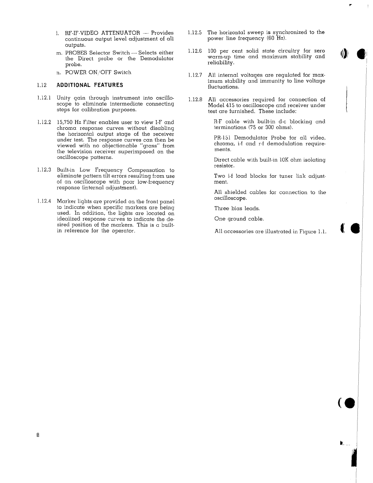
1.12
l. RF-IF-VIDEO ATTENUATOR - Provides
continuous output level adjustment of all
outputs.
m. PROBES Selector Switch - Selects either
the Direct probe or the Demodulator
probe.
n. POWER ON/OFF Switch
ADDITIONAL FEATURES
1.12.1 Unity gain through instrument into oscillo-
scope to eliminate intermediate connecting
steps for calibration purposes.
1.12.2 15,750 Hz Filter enables user to view 1-F and
chroma response curves without disabling
the horizontal output stage of the receiver
under test. The response curves can then be
viewed with no objectionable "grass" from
the television receiver superimposed on the
oscilloscope patterns.
1.12.3 Built-in Low Frequency Compensation to
eliminate pattern tilt errors resulting from use
of an oscilloscope with poor low-frequency
response (internal adjustment).
1.12.4 Marker lights are provided on the front panel
to indicate when specific markers are being
used. In addition, the lights are located on
idealized response curves to indicate the de-
sired position of the markers. This is a built-
in reference for the operator.
8
1.12.5 The horizontal sweep is synchronized to the
power line frequency (60 Hz).
1.12.6 100 per cent solid state circuitry for zero
warm-up time and maximum stability and
reliability.
1.12.7 All internal voltages are regulated for max-
imum stability and immunity to line voltage
fluctuations.
1.12.8 All accessories required for connection of
Model 415 to oscilloscope and receiver under
test are furnished. These include:
R-F cable with built-in d-c blocking and
terminations (75 or 300 ohms).
PR-151 Demodulator Probe for all video,
chroma, i-f and r-f demodulation require-
ments.
Direct cable with built-in lOK ohm isolating
resistor.
Two i-f load blocks for tuner link adjust-
ment.
All shielded cables for connection to the
oscilloscope.
Three bias leads.
One ground cable.
All accessories are illustrated in Figure 1.1.
..
O)J
e:e
ce

S-4911 Red Bias Lead (3 ea.) S-4912 Black Ground Lead
S-4918 1-FLoad Block (2 ea.)
S-4916 Mike Connector with Banana Plugs (2 ea.)
·~.t1'1~-~--~ L.___ -=L ~--- --r~
lliJ--;,.1--J._L - ----------
~~
S-4915 Cable witri lOK Ohm Isolating Resistor :..::s
(Black and Yellow Terminals)
PR-151 Demodulator Probe
TP-41
R-F Cable with Built-In
Termination (75 or 300 Ohms)
Figure Ll Accessories Furnished with the Model 415
9

2.0
2.1
10
TELEVISIONSIGNALSAND RECEIVERFUNCTIONS
TELEVISION SIGNAL PROCESSING
The following sections will first review the
transmitted television signal. Then the tele-
vision receiver will be reviewed with empha-
sis on the signal processing circuits. The
Model 415 circuitry will then be described.
Finally, the use of the 415 in receiver align-
ment will be described, first in general terms
and later in detail as we proceed into the
operating portion of the manual. Some
background information may be repeated in
several sections to maintain the continuity of
those sections.
THE TRANSMITTED TELEVISION SIGNAL
Before proceeding into the television receiver
description, a general review of the trans-
mitted television signal and its individual
components will be described.
The television channel spectrum is quite ex-
tensive. AU existing television channels are
listed in Table 2.1. Each channel occupies
six megahertz of the spectrum. The Pix and
Sound carrier frequencies for each channel
are also listed.
Figure 2.lA. shows the simplified television
frequency spectrum of Chanel 10 as broad-
cast by the television transmitter. The Chan-
nel band width is 6 MHz. The picture carrier
is 1.25 MHz above the lower limit of Channel
10. Within the channel, frequencies are ref-
erenced with respect to the picture carrier
frequency.
Notice that the I and Q signals are centered
on the Chroma center frequency of 196.83
MHz. The spectrum shows that the Q signal
sidebands are symmetrical about the chroma
center frequency with a distribution of ± 0.5
MHz. It is also indicated that the I signal
sidebands are not symmetrical about the
chroma center frequency, the upper side-
band spread being 0.5 MHz and the lower
sideband spread being 1.5 MHz. Early color
television receivers had a bandpass in the
chroma section which would pass the com-
plete bandwidth of the I and Q signals.
More modern color receivers have a band-
pass of ± 0.5 MHz for both the I and Q fre-
quency sidebands. This means that the por-
tion of the I signal outside the ± 0.5 MHz
bandpass is not utilized in the color television
receiver. Experience and comparison has
shown that picture quality is affected only
very slightly by deleting this portion of the
I signal spectrum. All modern color receivers
use the narrow band chroma response(± 0.5
MHz from the color subcarrier). The demod-
ulator matrices of the color-signal processing
circuits adjust the I and Q signal amplitudes
of the chroma information and generate a
phase shift of the chroma carrier (3.58 MHz)
with respect to the I and Q components so
that the B-Y and R-Y signal equivalents are
obtained. (The Y component is the mono-
chrome or black and white portion of the
television signal.) The B-Y and R-Y signals
are then combined to produce the resultant
G-Y signal. All three signals <R-Y,B-Y and
G-Y) are then applied to their respective am-
plifiers and from there to the picture tube of
the television receiver. The Y signal is also
added at this point so that the original Blue,
Red and Green signals are reproduced. Ex-
pressed as simple equations,
B-Y-l Y =B,
R-Y ~- Y =Rand
G-Y Y =G
Figure 2.lB. shows how the relative response
changes when the television signal is con-
verted to the intermediate frequency by the
tuner mixer and then passes through the i-f
stages.
In Figure 2.lB the i-f frequencies are indi-
cated with the corresponding Channel 10 r-f
frequencies (because the local oscillator of
the television receiver tuner operates above
the incoming television signal the order of
increasing frequency is reversed at the i-f
frequencies). For example, the center fre-
quency of the chroma information which is
196.83 MHz is 3.58 MHz above the picture
carrier which is 193.25 MHz. Similarly, the
sound carrier for Channel 10, which is
197.75 MHz, is 4.5 MHz above the picture
carrier frequency.
Referring to Figure 2.lB again, notice that at
the i-f frequencies the chroma center fre-
quency is 3.58 MHz below the picture carrier
frequency, which at the i-f frequencies is
45.75 MHz. Notice also that the sound carrier
frequency is 4.5 MHz below the picture car-
rier frequency. Later in the manual the i-f
frequency curve will be reversed so that in-
creasing frequencies are read from left to
right. In other words, the 39.75 MHz fre-
quency will be at the extreme left of the
frequency diagram and the 47.25 MHz signal
will be shown at the extreme right of the fre-
quency diagram. Throughout the manual it
will be conventional that all frequency dia-
grams show increasing frequency from left
to right.
Notice in Figure 2.lA that the sound carrier
of Channel 9, which is 191.75 MHz, is just
outside the lower end of the Channel 10
band. Also notice that the Channel 11 pix
carrier (199.25 MHz) is 1.25 MHz above the
upper band end of Channel 10. These two
frequencies are called the adjacent channel
sound carrier and the adjacent channel pix
carrier, respectively, of Channel 10.
(e

192
47.25
(191.75)
GN
<!a::zI
::eww::e
Ot-:::,r<>
a::z o<X>
IWww
uua::m
LL~
3.58 MHZ---..,..]
'
~UPPER VIDEO "", I
SIDEBANDS "" .
" "" ' ""
I
\. v
I
+0.5, -1.5 MHZ
1.25 MHZ i-,....,_ ______ 4.5MHz
45.75
(193.25)
I
194
CHANNEL 10
6 MHZ BANDWIDTH
I
195 I
196 I
197
42.17
(196.83)
l
198
41.25
(t97. 75)
B. Television Signal Spectrum Showing Response Variations Produced by
Processing the Signal Through the TV Receiver 1-FStages
Figure 2.1 Simplified Television Signal Spectrum (Channel 10)
I
199
39.75
(199.25)
11

Channel Freq.
No. Limits
p 55.25 2
S 59.75
-----
P 61.25
S 65.75 3
P 67.25
S 71.75 4
P 77.25
S 81.75 5
P 83.25
S 87.75 6
p 175.25 7
S 17_9_.7_5___ _
P 181.25
~5. 71__ 8__ _
p 187.25 9
S 191.75
----
p 193.25 10
S 197.75
p 199.25 11
S 203.75
p 205.25 12
S 209.75
p 211.25 13
S 215.75
-----
54
60
66
72
76
82
88
174
180
186
192
198
204
210
216
470
p 471.25 14
S 475.75 476
p 477.25 15
S 481.75 482
p 483.25 16
s 487.75 488
p 489.25 17
S 493.75 --- 494
p 495.25 18
S 499.75 500
p 501.25 19
S 505.75 506
p 507.25 20
S 511.75 512
p 513.25 21
S 517.75 518
p 519.25 22
S 523.75 524
p 525.25 23
S 529.75 530
p 531.25 24
S 535.75 536
p 537.25 25
S 541.75 542
Channel Freq.
No. Limits
542
p 543.25 26
S 547.75 548
p 549.25 27
S 553.75
p 555.25 28 554
S 559.75 560
p 561.25 29
S 56__5._75____ 566
p 567.25 30
S 571.75 572
p 573.25 31
s 577.75 578
p 579.25 32
S 583.75 584
p 585.25 33
S 589.75
----- 590
p 591.25 34
S 595.75 596
s 601.75 35
p 603.25 36
S 607.75
-----
p 609.25 37
S 613.75
p 615.25 38
S 619.75
p 621.25 39
S 625.75
S
p 627.25 40
631.75
P 633.25
S 637.75 41
602
608
614
620
626
632
638
s 643.75 42 644
P 645.25
s 649.7_5__ 43___650
p 651.25 44
S 655.75 656
P 657.25
s 661.75 45 662
P 663.25
s 667.75 46 668
P 669.25
s 673.75 47 674
p 675.25 48
S 679.75
------- 680
p 681.25 49
S 685.75 686
P 687.25
s 691.75 50 692
P 693.25
s 697.75 51 698
P 699.25
s 703.75 52 704
P 705.25
s 709.7_5_5_3__ 710
p 711.25 54
S 715.75
----- 716
Channel Freq.
No. Limits
------ 716
p 717.25 55
S 721.75
-P--72-3.-25____ 722
s 727.75 56 728
p 729.25 57
S 733.75
p735~2s - 5
-8
-734
S 739.75 740
p 741.25 59
5_7_4_5._75____ 746
p 747.25 60
S 751.75 --- 752
p 753.25 61
_S_75_7_.75____ 758
p 759.25 62
S 763.75 764
r-;:rr~--6-3-770
p 771.25 64
S 775.75 776
;___f;1Jt___
~~-
_182
P 783.25
§_}___87]5 66 788
P 789.25
s 793.75 - 67 -794
p 795.25 68
S 799.75 800
~r~f69 806
P 807.25
S 811.75
P 813.25
S 817.75
70
71
p 819.25 72
S 823.75
p 825~25__ 7_3_
S 829.75
p 831.25 74
S 835.75
P 837.25
S 841.75
P 843.25
S 847.75
75
76
p 849.25 77
S 853.75
-----------------
p 855.25 78
S 859.75
P 861.25
S 865.75
P 867.25
S 87I.75
79
80
p--873-.2-5__ 8_1_
S 877.75
p 879.25 82
S 883.75
r-~!~:~~83
812
818
824
830
836
842
848
854
860
866
872
878
884
890
P =Picture Carrier Freq. S =Sound Carrier Freq. All frequencies in MHz
12 TABLE2.1 Television Channel Frequency Spectrum
e
....
l ,
)
CH. 9 ----~---- CH. I0
186 192
--1--~_,..,..__CH.11 ---l
CH. II
ADJ
SND PlX
198
I
I
I
I
204
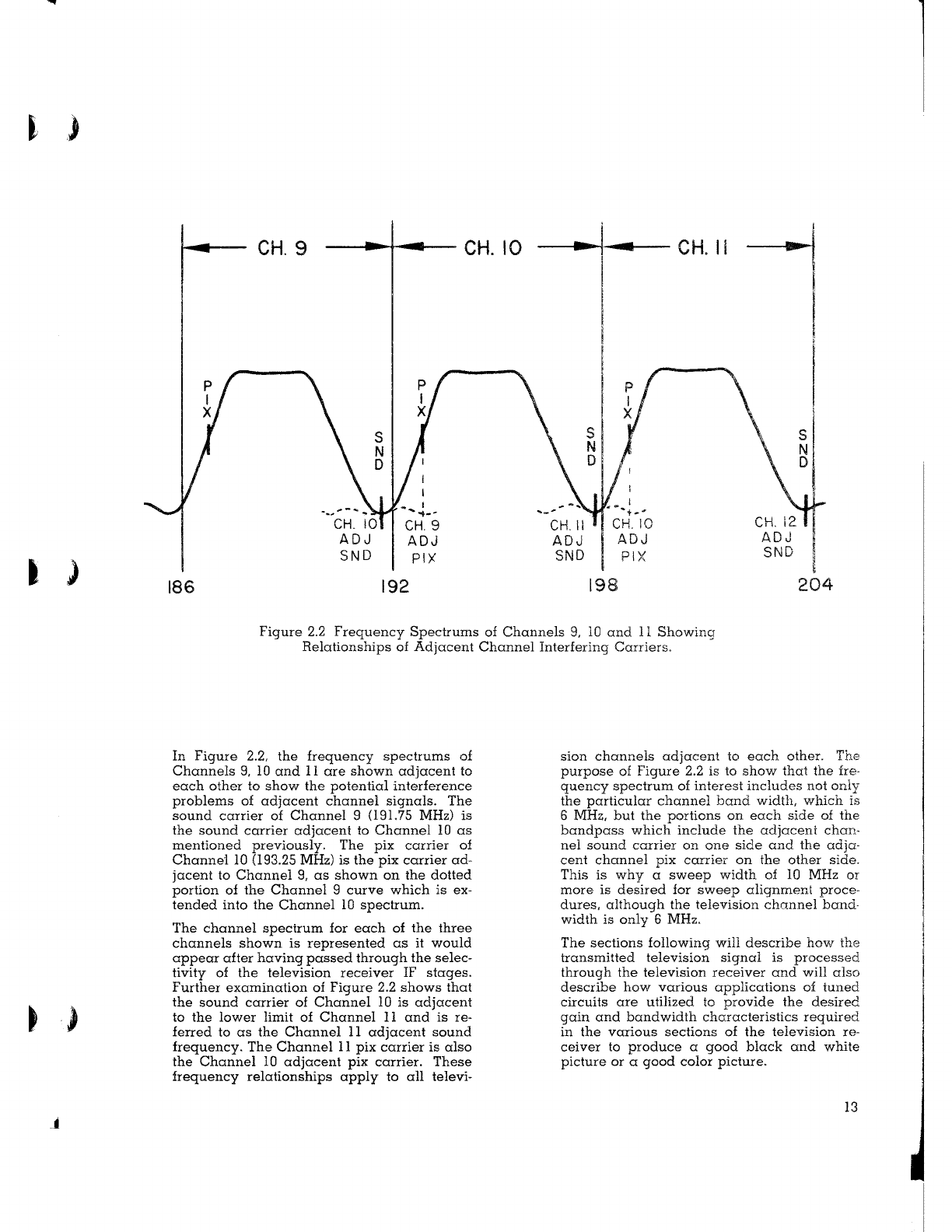
Figure 2.2 Frequency Spectrums of Channels 9, 10 and 11 Showing
Relationships of Adjacent Channel Interfering Carriers.
In Figure 2.2, the frequency spectrums of
Channels 9, 10 and 11 are shown adjacent to
each other to show the potential interference
problems of adjacent channel signals. The
sound carrier of Channel 9 (191.75 MHz) is
the sound carrier adjacent to Channel 10 as
mentioned previously. The pix carrier of
Channel 10 (193.25 MHz) is the pix carrier ad-
jacent to Channel 9, as shown on the dotted
portion of the Channel 9 curve which is ex-
tended into the Channel 10 spectrum.
The channel spectrum for each of the three
channels shown is represented as it would
appear after having passed through the selec-
tivity of the television receiver IF stages.
Further examination of Figure 2.2 shows that
the sound carrier of Channel 10 is adjacent
to the lower limit of Channel 11 and is re-
ferred to as the Channel 11 adjacent sound
frequency. The Channel 11 pix carrier is also
the Channel 10 adjacent pix carrier. These
frequency relationships apply to all televi-
sion channels adjacent to each other. The
purpose of Figure 2.2 is to show that the fre-
quency spectrum of interest includes not only
the particular channel band width, which is
6 MHz, but the portions on each side of the
bandpass which include the adjaceni chan-
nel sound carrier on one side and the adja-
cent channel pix carrier on the other side.
This is why a sweep width of 10 MHz or
more is desired for sweep alignment proce-
dures, although the television channel band-
width is only 6 MHz.
The sections following will describe how the
transmitted television signal is processed
through the television receiver and will also
describe how various applications of tuned
circuits are utilized to provide the desired
gain and bandwidth characteristics required
in the various sections of the television re-
ceiver to produce a good black and white
picture or a good color picture.
13

2.2 THE TELEVISION RECEIVER
The basic functions of the television receiver
are to select a specific television channel fre-
quency spectrum, process the signals, shape
the frequency spectrum as required by tuned
circuits (either bandpass or trap), demodulate
the frequency information and distribute the
demodulated signals to all the sound and
picture generating circuits. These circuits in-
clude vertical and horizontal sync, sound,
age, video, chroma circuits-all the circuits
following the detectors.
2.2.1 TYPICAL TELEVISION RECEIVER BLOCK
DIAGRAMS
Figure 2.3 depicts the block diagram of a rep-
resentative black and white television set,
whether solid-state, hybrid or tube-type. Fig-
ure 2.4 depicts a color set. Notice that a color
receiver is essentially a black-and-white set
with added circuitry for processing color pic-
ture information. Although the same color
signal is received by color as well as black-
and-white receivers, the black and white sets
simply do not use the color information.
Throughout this manual, emphasis is placed
on color receiver alignment because color
receiver alignment is more critical for proper
picture quality than is alignment in black
and white receivers. Black and white receiv-
r---;1
El
r:;,;l .J
IOUTPC.ITI
ers can, of course, be aligned by the methods
outlined in this manual, the difference being
that no chroma circuit alignment is required.
This means that only the responses obtained
at the video i-f detector and sound demodu-
lator are required.
The color receiver block diagram of Figure
2.4 can be simplified as shown in Figure 2.5
which groups the stages by major functions.
The circuit blocks which determine the gain
and bandwidth properties of the television
receiver are shown in Figure 2.6. These are
the circuits involved in sweep alignment. The
tuner selects the desired channel frequency
band, amplifies it and converts it down to the
i-f frequency. The tuner local oscillator op-
erates above the incoming signal frequency.
The mixer output of the tuner is coupled
through the tuner link to the first i-f amplifier.
Most of the response shaping and trapping
of undesired frequencies is done in the i-f
stages.
The i-f output is fed to the video detector and
the demodulated output of this stage is fed
to the video amplifier. From there it is fed
into the delay line and to the color amplifier
circuits. The color amplifiers have gain and
bandwidth characteristics which shape the
chroma information that is fed lo the color
demodulators.
Figure 2.3 Block Diagram of Typical Black and White Television Receiver
14
(
i

t )
I J
Figure 2.4 Block Diagram of Typical Color Television Receiver
@:,~,f--------""Tn
. [;_yl
-=:£f3L
tEMO;~TORS1[~::-tr~RTj
r---·-------·1 t
~~
COLOR CONTROLa~
'----------+-L __SYNC C!RCl.JITS_J
~
SYNC TlHORlZONTAL°l IH.V.REcr,REG~
DEFLECTIO-N ~1 r:ri;
~~~A~...I cTunsJ IFOCUS,OAM".ER
L:._._HORIZ OEfL COILS
- ----- '----- CONVERGEN(F.
VERTICA)B/ • : Vf'Rl DUL COi'"S
DEFLECTION, •
C!P~)JITS !----- f.ONVERGENCL
Figure 2.5 Simplified Television Receiver Block Diagram
RF
AGC IF
AGC
Figure 2.6 Signal Processing Circuits of Color Television Receiver
15
I
2.2.2 TELEVISION RECEIVER TUNED CIRCUITS
In order to process the signals properly the
r-f section and i-f section of the receiver must
possess certain gain and bandwidth charac-
teristics. These are determined by the num-
ber of amplifiers and the associated tuned
circuits.
The typical overall i-f bandpass curve is
shown in Figure 2.7 with a typical tuner re-
sponse curve superimposed. The i-f band-
pass is obviously narrower than the tuner
bandpass and therefore contributes most to
the bandpass shaping.
TUNER
RESPONSE
1-F
RESPONSE
ADJ~
PIX--
SOUND I ___ ADJ
SND
L--PJX
Figure 2.7 Typical Tuner and I-F Response Curves
Showing Relative Bandwidths
Figure 2.8 Overall Response of Stagger-Tuned Circuits
16
J I
'
I
'
~I
TRAP 1
:;
ATTEN '
' '
....t____'
RESPONSE
WITH TRAPS
OVERALL
~
1 RESPONSE
~
IWITHOUT TRAPS
:\
I
Figure 2.9 Effects of Trap Circuits on Overall
Response Curves
2.2.2.1 STAGGER-TUNED CIRCUITS
To obtain the bandwidth required in televi-
sion i-f amplifiers, stagger-tuned circuits must
be employed. This means that the outputs of
a series of stages tuned to different frequen-
cies are combined to obtain a desired overall
curve. This is demonstrated in Figure 2.8.
Assume that each individual response curve
(dotted lines) represents the output of a single
stage in a three-stage amplifier. The overall
response would be as indicated by the solid
outline. This is the response curve obtained
when a sweep-frequency generator is used.
2.2.2.2 TRAP FREQUENCY CIRCUITS
If it were desired to narrow the skirts of the
curve, additional stagger-tuned circuits could
be added, or specific trap frequency circuits
could be added to sharpen the slope re-
sponse. Because the trap is a highly selective
circuit the frequency "suck-out" will be sharp
and some flyback would occur outside the
trap frequency response. Figure 2.9 demon-
strates the overall effect. The dotted curve
outline is the curve of Figure 2.8 without fre-
quency traps. The solid curve is the result
of trap frequency circuit responses superim-
posed on the original. Idealized trap re-
sponses are shown in a downward direction.
Notice that outside the trap response region
the resultant curve approaches the original.
This flyback is evident in television i-f and
chroma response curves where traps are
used to reject undesired frequencies.
f

V
2.2.2.3 USE OF OVERCOUPLINGIN TUNED
CIRCUITS
Another method of obtaining a flat-top re-
sponse with tuned circuits is to overcouple.
If two tuned circuits are tuned to the same
frequency the overall response of the coils is
determined by the amount of coupling be-
tween them. Figure 2.10 shows typical curves
obtained by undercoupled, critically coupled
and overcoupled coils. In the overcoupled
case, the center dip in response willincrease
as the coupling is increased lei spread the
peaks. The maximum amplitudes will
also begin to decrease as overcoupling in-
creases. This principle is used in chroma
bandpass transformers. Usually, two tuning
slugs are found in these transformers. One
adjusts the coupling between windings and
the other is a tuning adjustment. Sweep
alignment of this type of transformer is prac-
tically a must. In this application as well as
in i-f alignment, a compromise between gain
and bandwidth is always made. The ampli-
tude of the response curve can be greatly
increased by tuning all adjustments for max-
imum amplitude, but this will be at a sacri-
fice in bandwidth which is equally important
in proper circuit performance.
CRITICALLY
COUPLED
I
OVERCOUPLED~-,.....,u.\L~......,UNDERCOUPLED
HEAVILY
_,,- OVERCOUPLED
Figure 2.10 Efiects of Coupling on Overall Response
of Two Tuned Circuits
A. Single Winding
B. Double Winding
Figure 2.11 Core Positions at Resonance in
Tunable Coil Assemblies
2.2.2.4 IMPORTANCEOFTUNING SLUG LOCATION
IN TUNED CIRCUITS
Regarding tuned circuits in general, it will
be noted that the alignment procedures spec-
ify the locations of the tuning slugs with
respect to the mounting board or chassis. In
designing the coil, the parameters are se-
lected so that the proper inductance value is
obtained when the tuning slug is between the
minimum and maximum inductance range of
the coil, rather than being at the maximum or
minimum point. This means that circuit res-
onance is obtained at two physical locations
of the coil (See Figure 2.llA) because at posi-
tion 1 the slug is surrounded by as many
turns of the coil as it is at position 2. Sup-
pose, however, that a secondary winding is
added at the bottom of the coil form as
shown in Figure 2.1IB. As in Figure 2.llA,
resonance is obtained at either position 1 or
2 of the tuning slug; however, at position 2
the presence of the slug in a portion of the
primary and secondary of the assembly in-
creases the coupling between the two wind-
ings as compared to the coupling obtained
with the slug at position 1. The amount of
coupling afiects gain and bandwidth; there-
fore, to obtain the desired coil or transformer
characteristics the slug must be properly
17
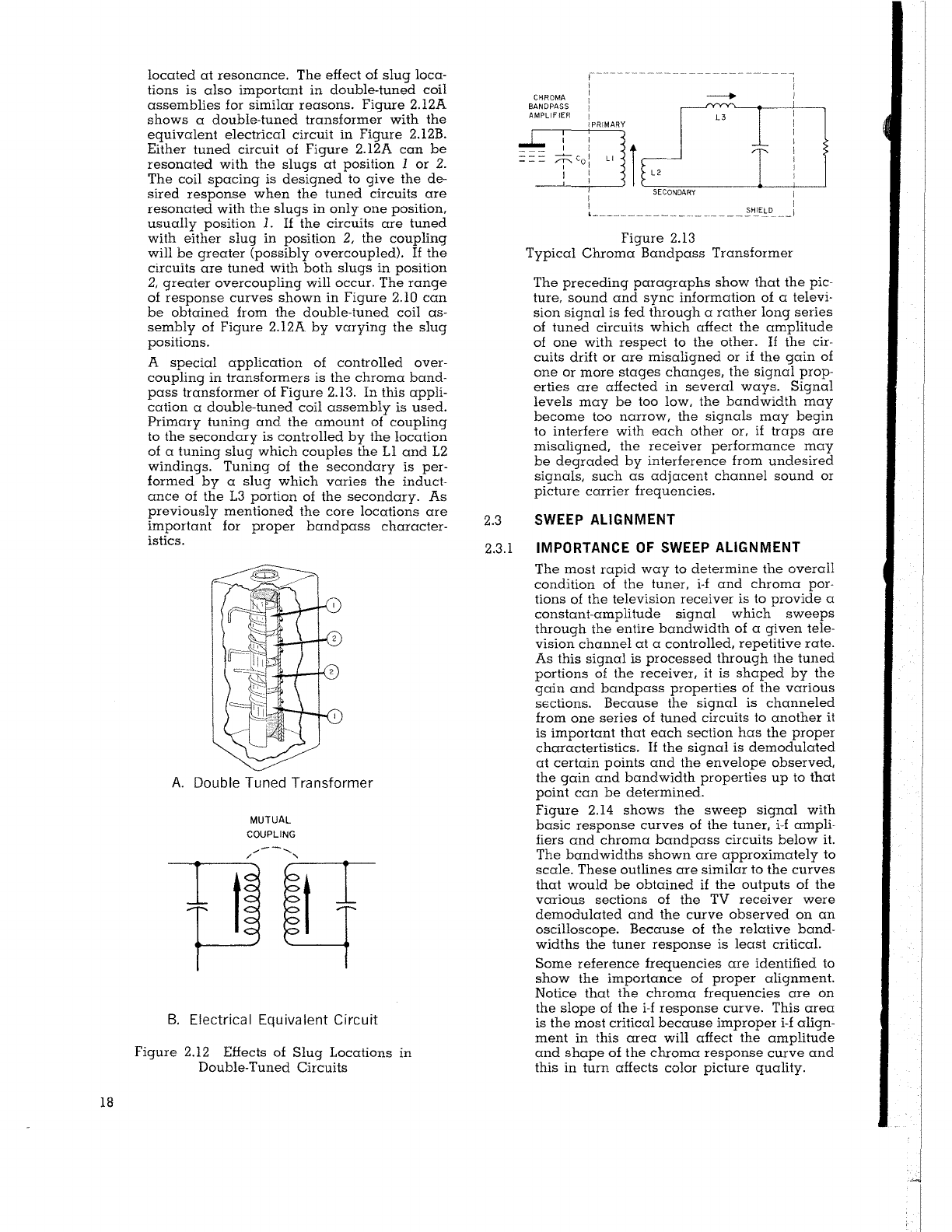
18
located at resonance. The effect of slug loca-
tions is also important in double-tuned coil
assemblies for similar reasons. Figure 2.12A
shows a double-tuned transformer with the
equivalent electrical circuit in Figure 2.12B.
Either tuned circuit of Figure 2.12A can be
resonated with the slugs at position 1 or 2.
The coil spacing is designed to give the de-
sired response when the tuned circuits are
resonated with the slugs in only one position,
usually position 1. If the circuits are tuned
with either slug in position 2, the coupling
will be greater (possibly overcoupled). If the
circuits are tuned with both slugs in position
2, greater overcoupling will occur. The range
of response curves shown in Figure 2.10 can
be obtained from the double-tuned coil as-
sembly of Figure 2.12A by varying the slug
positions.
A special application of controlled over-
coupling in transformers is the chroma band-
pass transformer of Figure 2.13. In this appli-
cation a double-tuned coil assembly is used.
Primary tuning and the amount of coupling
to the secondary is controlled by the location
of a tuning slug which couples the Ll and 12
windings. Tuning of the secondary is per-
formed by a slug which varies the induct-
ance of the 13 portion of the secondary. As
previously mentioned the core locations are
important for proper bandpass character-
istics.
A. Double Tuned Transformer
MUTUAL
COUPLING
.,,,,--.......
/ '
t t
B. Electrical Equivalent Circuit
Figure 2.12 Effects of Slug Locations in
Double-Tuned Circuits
Figure 2.13
Typical Chroma Bandpass Transformer
The preceding paragraphs show that the pic-
ture, sound and sync information of a televi-
sion signal is fed through a rather long series
of tuned circuits which affect the amplitude
of one with respect to the other. If the cir-
cuits drift or are misaligned or if the gain of
one or more stages changes, the signal prop-
erties are affected in several ways. Signal
levels may be too low, the bandwidth may
become too narrow, the signals may begin
to interfere with each other or, if traps are
misaligned, the receiver performance may
be degraded by interference from undesired
signals, such as adjacent channel sound or
picture carrier frequencies.
2.3 SWEEP ALIGNMENT
2.3.l IMPORTANCE OF SWEEP ALIGNMENT
The most rapid way to determine the overall
condition of the tuner, i-f and chroma por-
tions of the television receiver is to provide a
constant-amplitude signal which sweeps
through the entire bandwidth of a given tele-
vision channel at a controlled, repetitive rate.
As this signal is processed through the tuned
portions of the receiver, it is shaped by the
gain and bandpass properties of the various
sections. Because the signal is channeled
from one series of tuned circuits to another it
is important that each section has the proper
charactertistics. If the signal is demodulated
at certain points and the envelope observed,
the gain and bandwidth properties up to that
point can be determined.
Figure 2.14 shows the sweep signal with
basic response curves of the tuner, i-f ampli-
fiers and chroma bandpass circuits below it.
The bandwidths shown are approximately to
scale. These outlines are similar to the curves
that would be obtained if the outputs of the
various sections of the TV receiver were
demodulated and the curve observed on an
oscilloscope. Because of the relative band-
widths the tuner response is least critical.
Some reference frequencies are identified to
show the importance of proper alignment.
Notice that the chroma frequencies are on
the slope of the i-f response curve. This area
is the most critical because improper i-f align-
ment in this area will affect the amplitude
and shape of the chroma response curve and
this in turn affects color picture quality.
Table of contents
Other B&K Portable Generator manuals


