BIOS M9B User manual

C h a p t e r 1
System Introduction
System Introduction 1-1
1.1 Overview
1.1.1 System Board
The M9B is a dual-processor system board that supports the Intel Pentium Pro CPU. It contains
an exclusive slot for the Pentium Pro CPU board that carries two zero-insertion force (ZIF) CPU
sockets.
This high-performance 64-bit system board utilizes both the EISA and the PCI local bus
architecture. Two EISA, four PCI bus slots, and one EISA/PCI shared slot reside on the board to
allow installation of either master or slave devices.
The system board has four DRAM banks composed of eight 72-pin SIMM sockets that
accommodate both fast-page mode and EDO (extended data output) SIMMs. The sockets support
a total of 256-MB system memory using 32-MB SIMMs.
A 50-pin Fast SCSI-II interface and a 68-pin Wide SCSI interface come with the system board to
connect SCSI devices. Standard external I/O interfaces include two 9-pin serial ports, one parallel
port, a video port, and keyboard and mouse ports.
The system board supports two optional features, the ASM Pro and the remote diagnostic
management (RDM), that allow better server management. The ASM Pro detects problems in
CPU thermal condition, 5V/3.3V/1.5V detection, and PCI bus utilization calculation. The RDM
allows execution of the RDM diagnostic program from a remote RDM station to fix detected
problems or to reboot the system.
1.1.2 CPU Board
The Pentium Pro CPU board carries two ZIF sockets (Socket 8) to accommodate the new Pentium
Pro CPUs running at 180 MHz and 200 MHz.
The board also includes the PCI bridge/memory controller (PMC) and the data bus
accelerator (DBX) chipsets. The PMC provides bus control signals and address paths for transfers
between the host bus, PCI bus, and the main memory. The DBX supoorts multiple-bit error
detection and sigle-bit error correction through the ECC/parity feature.

1-2Service Guide
1.1.3 Features
The M9B system has the following features:
•A separate CPU board that carries the Pentium Pro CPU and the 512-KB synchronous
pipeline burst second-level cache
•Four PCI slots, two EISA slots, and one PCI/EISA shared slot, with all PCI slots supporting
master devices
•Four DRAM banks composed of eight 72-pin SIMM sockets that support 8/16/32-MB
70ns fast-page mode or EDO-type SIMMs
•Fast SCSI and Wide SCSI interfaces
•Standard 1-MB video DRAM onboard plus two upgrade sockets for up to 2-MB video memory
•256-KB Flash ROM BIOS
•System clock/calendar with 8KB CMOS RAM with battery backup
•Onboard interfaces for front panel LED and backplane board SCSI HDD status indicator
•ASM Pro and remote diagnostic management (RDM) features
•Power management features (IDE hard disk standby mode and system suspend mode)
•External ports:
•PS/2 keyboard and mouse ports
•Two buffered high-speed serial ports (NS16C550-compatible UARTs with 16-byte FIFOs)
•One ECP/EPP high-speed parallel port (IEEE 1284-compliant)
•Video port
•Onboard controller chipsets
•Cache/memory/buffer controller (82439HX)
•EISA System Component (ESC 82374SB)
•PCI-EISA Bridge (PCEB 82375SB)
•SCSI controller (AIC 7880)
•PCI-to-PCI Bridge (DEC 21052)
•Super I/O controller (SMC 37C665)
•PCI local bus VGA with enhanced GUI acceleration (ATI 264CT)

System Introduction 1-3
1.2 Board Layouts
1.2.1 System Board
1 COM1
2 COM2
3 Mouse port
4 Keyboard port
5 Video port
6 Parallel port
7 Video RAM upgrade sockets
8 CPU board slot
9 PCI slots
10 EISA slots
11 Real-time clock
12 Flash ROM BIOS
13 Buzzer
14 Narrow SCSI connector
15 Wide SCSI connector
16 SIMM sockets
17 Fan connector 1 (FA1)
18 Fan connector 2 (FA2)
19 Fan connector 3 (FA3)
20 Power connector
21 Power connector
22 Video RAM
23 RDM connectors
Figure 1-1 System Board Layout
3
6
1
2
5
8
9
10
19
18
17
20
21
23
15
14
12
13
11
16
22
4
7

1-4Service Guide
1.2.1 CPU Board
Figure 1-2 CPU Board Layout
Fan1
CPU 2 Socket
CPU Voltage Regulators
Fan2
CPU 1 Socket
VRM Socket
VRM Socket

System Introduction 1-5
1.3 Jumpers and Connectors
Figure 1-3 System Board Jumper and Connector Locations
Figure 1-4 CPU Board Jumper Locations
CN3 CN1 CN2
J16
1-6Service Guide
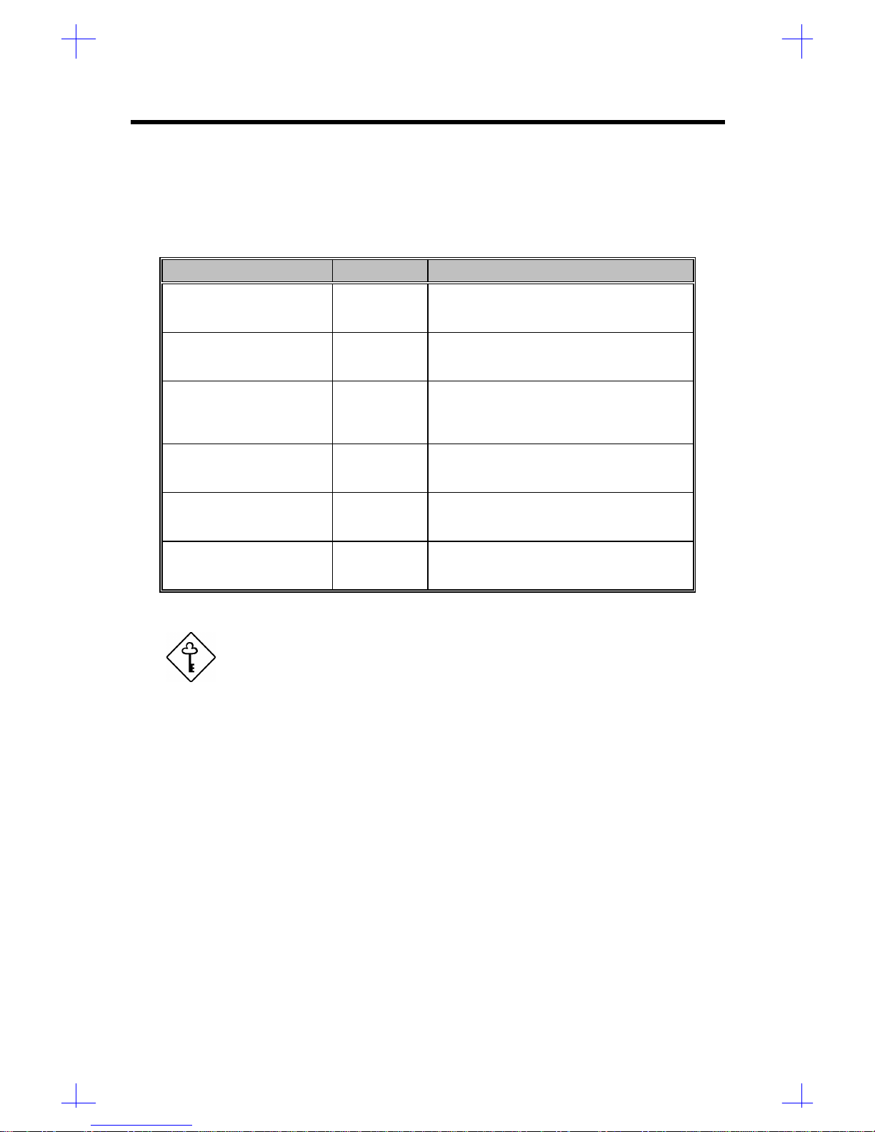
1.3.1 Jumper Settings
System Board
Table 1-1 System Board Jumper Settings
Jumper Setting Function
Password Security
JP1 1-2
2-3 Check password
Bypass password
BIOS Type
JP2 1-2
2-3 Acer
OEM
SCSI Termination
JP3 1-2
2-3 Terminator always set to ON
Use SCSI Setup Utility to set terminator to
ON or OFF
SCSI Feature
JP4 1-2
2-3 Wide SCSI
Standard
Hardware Reset
JP5 1-2
2-3 Enabled
Disabled
Sound Feature
JP6 1-2
2-3 Buzzer
Speaker
If both narrow and wide SCSI interfaces are present, set JP4 to
pins 1-2 for wide SCSI function.
System Introduction 1-7
CPU Board
Table 1-2 CN1 Settings for CPU Core/Bus Frequency Ratio
CN1 Settings CPU Core /
1-5 2-6 3-7 4-8 Bus Freq. Ratio
1 1 1 1 2
1 1 0 1 3
1 1 1 0 4
1 1 0 0 5
0 1 1 1 2.5
0 1 0 1 3.5
0 - Pins open 1 - Pins Closed
Table 1-3 lists the CPU core voltages depending on CN2 and CN3 settings.
Table 1-3 CN2 and CN3 Settings for CPU Core Voltage
CN2/CN3 Settings
1-5 2-6 3-7 4-8 CPU Voltage
1 1 1 1 3.5
1 1 1 0 3.4
1 1 0 1 3.3
1 1 0 0 3.2
1 0 1 1 3.1
1 0 1 0 3.0
1 0 0 1 2.9
1 0 0 0 2.8
0 1 1 1 2.7
0 1 1 0 2.6
0 1 0 1 2.5
0 1 0 0 2.4
0 0 1 1 2.3
0 0 1 0 2.2
0 0 0 1 2.1
0 0 0 0 Reserved
0 - Pins open 1 - Pins Closed
Table 1-4 Clock Settings
J16 CPU
1-2 2-3 Clock Speed
1 0 60 MHz
0 1 66 MHz
0 - Pins open 1 - Pins Closed
1-8Service Guide
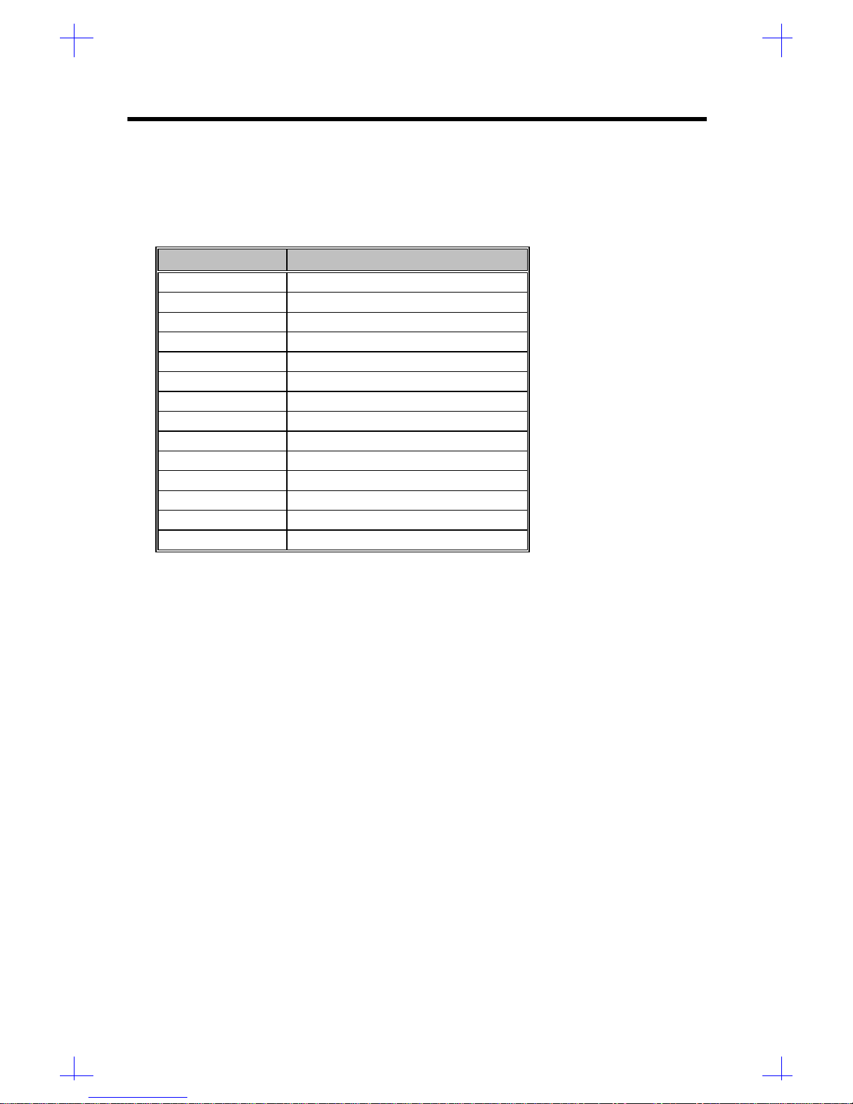
1.3.2 Connector Functions
Table 1-5 lists the different connectors on the system board and their respective functions.
Table 1-5 System Board Connectors
Connector Function
CN1 Power connector
CN2 Power connector
CN3 Backplane board HDD status connector
CN5 IDE hard disk connector
CN6 RDM connector
CN7 RDM connector
CN8 Diskette drive connector
CN11 68-pin Wide SCSI connector
CN12 50-pin Fast SCSI-II connector
CN13 RDM cable and LED board connector
CN14 Hard disk LED connector
CN15 Power LED connector
CN16 Speaker connector
SW1 NMI switch

System Introduction 1-9
1.4 System Specifications
Table 1-6 System Specifications
Item Description
CPU P54C/P55C, 100/120/133/150/166/200 MHz
System Memory Eight SIMM sockets that support up to 256 MB of system memory
using 60/70ns 4/8/16/32-MB SIMMs1.
Video Memory Onboard 1-MB (256K16x2) video memory upgradable to 2-MB by
installing another two pieces of 256K16 70ns SOJ chip into the
upgrade socket
Cache Onboard 512-KB synchronous pipeline burst second-level cache
data SRAM chip (32K32x4)
Onboard 64-KB tag SRAM chip (32K8x2)
BIOS2256-KB Flash ROM for system, SCSI and video BIOS
Video interface Onboard ATI264CT PCI accelerator that supports a resolution of
1024x768, 65536 color interlaced with 2-MB video RAM.
Hard Disk Interface IDE interface supports up to two IDE devices
PCI bus master fast SCSI II interface supports up to seven devices
or fifteen SCSI devices when wide SCSI is used.
Diskette Drive Interface One diskette drive interface that supports 2.88/1.44/1.2-MB
diskette drives
Supports three-mode diskette type
Onboard I/O One PS/2 keyboard port (6-pin, mini-din type x1)
One PS/2 mouse port (6-pin, mini-din type x1)
Two NS16C550-compatible serial ports (9-pin D-type x2)
One ECP/EPP parallel port (15-pin D-type x1)
Real-time Clock System clock/calendar with 128 bytes extended CMOS RAM and
battery backup
Expansion slots One CPU board slot
Two first-level PCI bus slot (master/slave)
Two second-level PCI bus slot (master/slave)
Two EISA bus slot (master/slave)
One first-level PCI/EISA shared bus slot (master/slave)
Power Supply 525/350/200-watt switching power supply
Housings IDUN or IDATX housing
1Supports both traditional fast-page mode and EDO mode SIMMs.
2Supports PCI v2.1, PnP v1.0a, and APM v1.1 protocols.
1-10 Service Guide
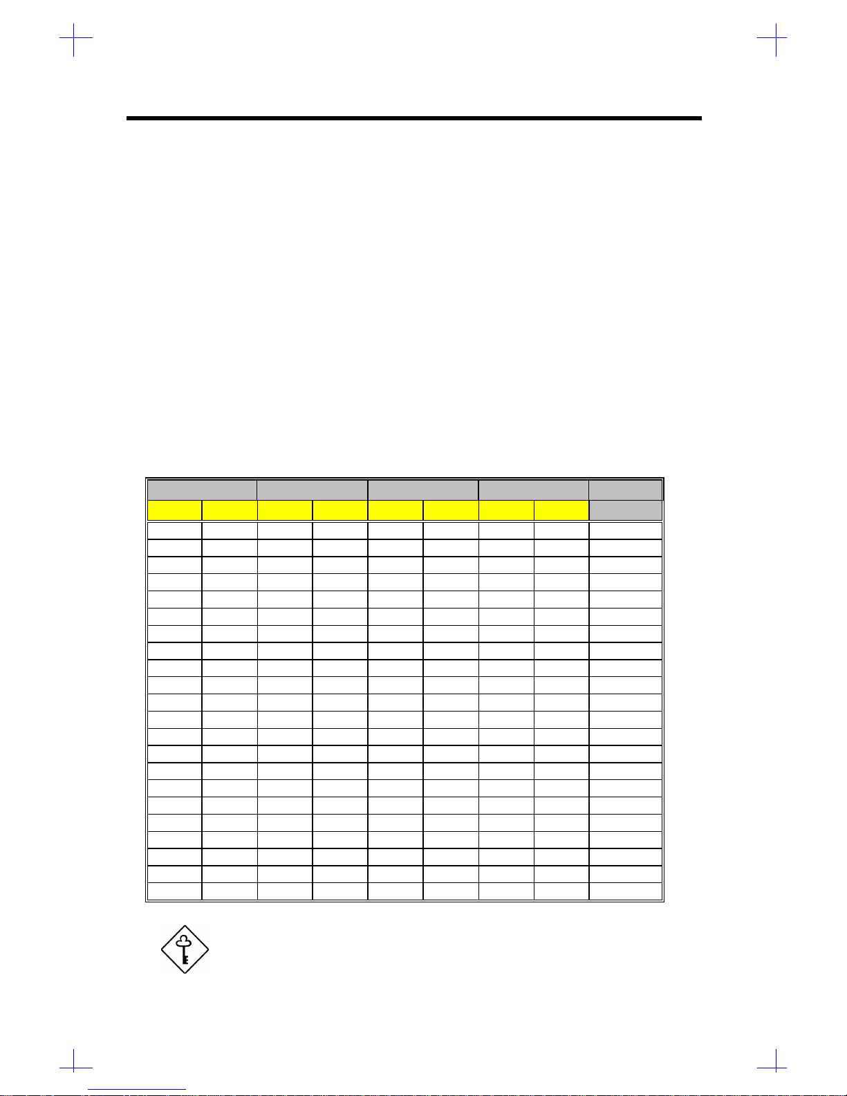
1.5 Hardware Configurations
1.5.1 Memory Configurations
The system board comes with eight 72-pin SIMM sockets that support 4-MB and 16-MB single-
density SIMMs as well as 8-MB and 32-MB double-density SIMMs for a total system memory of
256-MB. The sockets support both the fast page mode and EDO 60/70 ns SIMMs.
Rules for Adding Memory
•You may use the memory banks (Bank0 ~Bank3) in any order.
•Use only one type of SIMM in a given bank. You may combine EDO or fast-page mode
SIMMs for a memory configuration as long as the SIMMs in each bank are of the same type.
•Use only SIMMs with the same capacity in a bank. For example, do not combine 8-MB and
16-MB SIMMs in a bank.
•Always install SIMMs in pairs. For example, for a total memory of 16 MB, install two 8-MB
SIMMs in a bank. You can not use a 16-MB SIMM alone for a 16-MB memory.
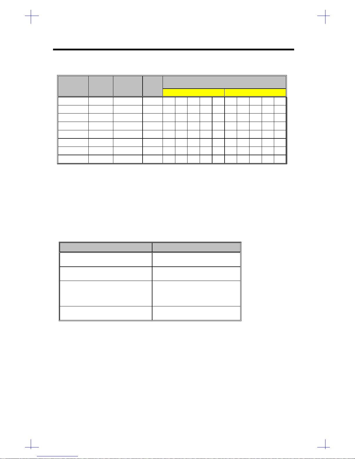
Table 1-7 Memory Configurations
Bank0 Bank1 Bank2 Bank3 Total
S1 S2 S3 S4 S5 S6 S7 S8 Memory
8 MB 8 MB 16 MB
16 MB 16 MB 32 MB
32 MB 32 MB 64 MB
8 MB 8 MB 16 MB
16 MB 16 MB 32 MB
32 MB 32 MB 64 MB
8 MB 8 MB 8 MB 8 MB 32 MB
16 MB 16 MB 16 MB 16 MB 64 MB
32 MB 32 MB 32 MB 32 MB 128 MB
8 MB 8 MB 16 MB 16 MB 48 MB
8 MB 8 MB 32 MB 32 MB 80 MB
16 MB 16 MB 32 MB 32 MB 96 MB
8 MB 8 MB 16 MB 16 MB 48 MB
8 MB 8 MB 16 MB 16 MB 16 MB 16 MB 80 MB
8 MB 8 MB 16 MB 16 MB 32 MB 32 MB 112 MB
8 MB 8 MB 16 MB 16 MB 32 MB 32 MB 32 MB 32 MB 176 MB
8 MB 8 MB 8 MB 8 MB 16 MB 16 MB 16 MB 16 MB 96 MB
8 MB 8 MB 8 MB 8 MB 32 MB 32 MB 32 MB 32 MB 160 MB
16 MB 16 MB 16 MB 16 MB 32 MB 32 MB 32 MB 32 MB 192 MB
8 MB 8 MB 8 MB 8 MB 8 MB 8 MB 8 MB 8 MB 64 MB
16 MB 16 MB 16 MB 16 MB 16 MB 16 MB 16 MB 16 MB 128 MB
32 MB 32 MB 32 MB 32 MB 32 MB 32 MB 32 MB 32 MB 256 MB
The above configurations are only some of the available memory
combinations. You can use other combinations as long as you
follow the above rules for upgrading memory.

System Introduction 1-11
1.5.2 Second-level Cache Configurations
The 512-KB pipeline burst second-level cache consists of four pieces of SRAM chips located on
the CPU board (U3~U6).
1.5.3 Video RAM Configurations
The system comes with a 1-MB onboard video RAM composed of two 514260ASL (256Kb x 16,
70ns SOJ) chips. The video RAM is upgradable to 2 MB by adding two more 514260ASL chips
into the video RAM upgrade sockets labeled U18 and U21 (see Figure 1-1 for the location).
1.5.4 Video Display Modes
Table 1-8 shows the video display modes using 45ns video RAM.
Table 1-8 Video Display Modes
Display
Resolution Refresh
Rate Horizontal
Frequency Pixel
Clock Colors (Bits / Pixel)
(Hz) (KHz) (MHz) 1MB DRAM 2MB DRAM
640*480 60 31.4 25.2 4 8 16 24 32 4 8 16 24 32
640*480 60 31.4 25.2 üüüü- üüüüü
640*480 72 37.7 31.2 üüüü- üüüüü
640*480 75 37.5 31.5 üüüü- üüüüü
640*480 90 47.9 39.9 üüü- - üüü- -
640*480 100 52.9 44.9 üüü- - üüüü-
800*600 48 int. 33.8 36.0 - üü- - - üüü-
800*600 56 35.1 36.0 üüü- - üüüü-
800*600 60 37.8 40.0 üüü- - üüü- -
800*600 70 44.5 44.9 üüü- - üüü- -
800*600 72 48.0 50.0 üüü- - üüü- -
800*600 75 46.8 49.5 üüü- - üüü- -
800*600 90 57.0 56.6 üü- - - üü- - -
800*600 100 62.5 67.5 üü- - - üü- - -
1024*768 43 int. 35.5 44.9 üü- - - üüü- -
1024*768 60 48.3 65.0 üü- - - üüü- -
1024*768 70 56.4 75.0 üü- - - üüü- -
1024*768 72 58.2 75.0 üü- - - üüü- -
1024*768 75 60.0 78.8 üü- - - üüü- -
1024*768 90 76.2 100 - - - - - üü- - -
1024*768 100 79.0 110 - - - - - üü- - -
1152*864 43 int. 45.9 65.0 üü- - - üü- - -
1152*864 47 int. 44.8 65.0 üü- - - üü- - -
1152*864 60 54.9 80.0 üü- - - üü- - -
1152*864 70 66.1 100 - - - - - üü- - -
1-12 Service Guide
Table 1-8 Video Display Modes (continued)
Display
Resolution Refresh
Rate Horizontal
Frequency Pixel
Clock Colors (Bits / Pixel)
(Hz) (KHz) (MHz) 1MB DRAM 2MB DRAM
1152*864 75 75.1 110 - - - - - üü- - -
1152*864 80 75.1 110 - - - - - üü- - -
1280*1024 43 int. 50.0 80.0 ü- - - - üü- - -
1280*1024 47 int. 50.0 80.0 ü- - - - üü- - -
1280*1024 60 63.9 110 - - - - - üü- - -
1280*1024 70 74.6 126 - - - - - üü- - -
1280*1024 74 78.8 135 - - - - - üü- - -
1280*1024 75 79.9 135 - - - - - üü- - -
int. - interlaced
1.5.5 Parallel Port Configurations
The onboard parallel port interface supports a 25-pin D-type connector. The port functions in
different operation modes and is adjustable to select LPT1, LPT2, and LPT3 by changing the
CMOS settings in the BIOS Utility.
Table 1-9 lists the operation mode settings and their corresponding functions.
Table 1-9 Parallel Port Operation Mode Settings
Setting Function
Standard Parallel Port (SPP) Allows normal speed operation but in
one direction only
Enhanced Parallel Port (EPP 1.7/1.9) Allows bidirectional parallel port
operation at maximum speed
Extended Capabilities Port (ECP) Allows parallel port to operate in
bidirectional mode and at a speed
higher than the maximum data
transfer rate
Standard and Bidirectional Allows normal speed operation in a
two-way mode
1.5.6 Serial Port Configurations
The system board has two high-speed 9-pin D-type serial ports. These ports are NS16C550-
compatible UARTs with 16-byte FIFO send/receive capability. The port functions are software
adjustable to select COM1, COM2, COM3, and COM4.
1.5.7 IDE Interface Configurations
The system board includes PCI enhanced local bus IDE interfaces that accommodate up to four
IDE devices. The interfaces functions as PCI bus master IDE and support PIO mode-4 and DMA
mode-2. The interfaces are fully compatible with ANSIS ATA Rev. 3.0 specifications and ATAPI
specifications.
System Introduction 1-13
1.5.8 Memory Address Map
Table 1-10 Memory Address Map
Address Size Function
0000000 ~ 009FFFF 640 KB system memory Onboard DRAM
00A0000 ~ 00BFFFF 128 KB video RAM Reserved for graphics display buffer,
non-cacheable
00C0000 ~ 00C7FFF 32 KB for VGA BIOS Reserved for onboard VGA
00C8000 ~ 00CFFFF 32 KB I/O expansion ROM Reserved for ROM on I/O adapters
00D0000 ~ 00D3FFF 16 KB I/O expansion ROM Reserved for ROM on I/O adapters
00D4000 ~ 00D7FFF 16 KB I/O expansion ROM Reserved for ROM on I/O adapters
00D8000 ~ 00DBFFF 16 KB I/O expansion ROM Reserved for ROM on I/O adapters
00DC000 ~ 00DFFFF 16 KB I/O expansion ROM Reserved for ROM on I/O adapters
00E0000 ~ 00E7FFF 32 KB for SCSI BIOS Reserved SCSI BIOS
00E8000 ~ 00EFFFF 32 KB Reserved onboard (video RAM BIOS)
00F0000 ~ 00FFFFF 64 KB BIOS System ROM BIOS (ROM)
System RAM BIOS (DRAM)
0100000 ~ 0F9FFFF System memory Onboard DRAM
0FA0000 ~ 0FFFFFF 384 KB I/O card memory Reserved for memory map I/O card,
non-cacheable
1000000 ~ Upper limit1System memory Onboard DRAM
1.5.9 PCI INTx# Map
Table 1-11 PCI INTx# Map
PCI Bus# PCI INTx PCI Device
PCI Bus 0 INTA AIC-7880 SCSI; PCI slot s1, 2
INTB PCI slots 1, 2
INTC PCI slots 1, 2
INTD PCI slots 1, 2
PCI Bus 1 INTA PCI slots 3, 4, 5
INTB PCI slots 3, 4, 5
INTC PCI slots 3, 4, 5
INTD PCI slots 3, 4, 5
1Upper limit means the maximum size of main memory.

1-14 Service Guide
1.5.10 Interrupt Channels Map
Table 1-12 Interrupt Channels Map
IRQ System Device
IRQ0 Timer output 0
IRQ1 Keyboard
IRQ2 Reserved
IRQ3 Serial port 2
IRQ4 Serial port 1
IRQ5 Reserved
IRQ6 Diskette drive
IRQ7 Parallel port
IRQ8 Real-time clock
IRQ9 Reserved
IRQ10 Reserved
IRQ11 Reserved
IRQ12 PS/2 mouse
IRQ13 Math coprocessor
IRQ14 IDE hard disk
IRQ15 Reserved
1.5.11 DMA Channels Map
Table 1-13 DMA Channels Map
Channel Function
0Available
1Available
2Floppy Controller
3Available
4Cascaded
5Available
6Available
7Available
System Introduction 1-15
1.5.12 I/O Address Map
Table 1-14 I/O Address Map
Hex Range Device
000 ~ 01F DMA controller 1, (8237)
020 ~ 027 Interrupt controller 1, (8259)
030 ~ 037 Interrupt controller 1, (8259)
040 ~ 047 System timer (8254-1)
050 ~ 057 System timer (8254-1)
060 ~ 06F Keyboard controller (8742)
070 ~ 07F Real-time clock, NMI mask
080 ~ 09F DMA page register 74LS612, speed status register
0A0 ~ 0BF Interrupt controller 2, (8259)
0C0 ~ 0DF DMA controller 2, (8237)
0F0 Clear math coprocessor busy
0F1 Reset math coprocessor
0F8 ~ 0FF Math coprocessor
4F01Onboard VGA enabled/disable
Flash ROM programming
RDM reset
DMA channel 1 selection
DMA channel 3 selection
4F11ASM data read/write port
IRQ mapper read/write port
4F21ASM index write port
IRQ mapper index read/write port
0CF8 PCI configuration address regulation
0CFC PCI configuration data regulation
1F0 ~ 1F7 Hard disk
278 ~ 27F Parallel port 2
2F8 ~ 2FF Serial port 2
378 ~ 37F Parallel port 1
3B0 ~ 3BF Monochrome display
3C0 ~ 3CF EGA, VGA, SVGA
3D0 ~ 3DF CGA, VGA, SVGA
3F0 ~ 3F7 Diskette drive controller
3F7 ~ 3FF Serial port 1
1Special I/O port

1-16 Service Guide
1.6 System Block Diagram
Figure 1-7 System Block Diagram

System Introduction 1-17
Figure 1-8 System Clock Block Diagram

1-18 Service Guide
1.7 Operation Theory
1.7.1 Memory Address Structure
M9B is a Pentium Pro system based on 440FX PCIset supports 4GB of addressable memory
space and 64 KB of addressable I/O space. The Pentium Pro processor family supports
addressing of memory ranges larger than 4GB via the REQa[4:0]# signals (see Chapter 4 for
details). The PMC claims any access over 4GB by terminating transaction (without forwarding it to
the PCI bus). Writes are terminated simply by dropping the data and the PMC returns all zeros for
reads.
15M
1M
640K512K
0M
Extended
ISA
Memory
DOS
Compatible
Memory
and
Buffer Area
(128KB)
Optional
Fixed
Memory
Hole
(128KB)
DOSArea
(512KB)
768KB640KB512KB
Standard
PCI/ISA
Video
Memory
Area
(128KB)0C0000h0BFFFFh0A0000h09FFFFh080000h07FFFFh000000h
Figure 1-9 Memory Address Structure
DOS Area (0000-9FFFFh)
The DOX area is 640KB in size and it is further devided into two parts. The 512KB area at 0 to
7FFFFh is always mapped to the main memory controlled by the PMC, while the 128KB address
range from 080000 to 09FFFFh can be mapped to PCI or to main DRAM. By default this range is
mapped to main memory and can be diclared as a main memory hole by BIOS CMOS setup.
Video Buffer Area (A0000-BFFFFh)
The 128KB graphics adapter memory region in normally mapped to a video device on the PCI bus
(typically VGA controller). This region is also the default region for SMM space.

System Introduction 1-19
Expansion Area (C0000-DFFFFh), Extended System BIOS Area (E0000-EFFFFh)
This two areas can be assigned as shadow or disable(read/write for other use, not shadow for
expansion ROM BIOS use) states by BIOS CMOS setup. By manipulating the shadow attributes,
the PMC can “shadow” the expansion ROM BIOS into the main DRAM Typically, these blocks
are mapped through the PCI bridge to ISA space. Memory that is disabled is not remapped.
System BIOS Area (F0000-FFFFFh)
This area is a single 64KB segment. This segment can be assigned as shadow or disable
(read/write for other use, not shadow for system BIOS use) states by BIOS CMOS setup. By
manipulating the shadow attributes, the PMC can “shadow” system BIOS into the main DRAM.
Memory that is disabled is mot remapped.
Extended Memory Area
This memory area covers 100000h (1 MB) to FFFFFFFFh (4GB minus 1) address range and it is
devided into the following regions:
•DRAM memory from 1 MB to a Top of Memory
•PCI memory space from the Top of Memory to 4GB with two specific ranges
•APIC Configuration Space from FEC00000h (4GB minus 20 MB) to FEC0_FFFFh
•High BIOS area from 4GB to 4GB minus 2 MB
DRAM memory from 1 MB to a Top of Memory
The address range from 1 MB to the top of main memory is mapped to main DRAM address range
controlled by PMC. All accesses to addresses within this range are forwarded by the PMC to the
DRAM unless a hole in this range is created by BIOS CMOS setup.
PCI memory space from the Top of Memory to 4GB with two specific ranges
The address range from the top of main DRAM to 4GB is normally mapped to PCI. The PMC
forwards all accesses within this address range to PCI.
There are two sub-ranges within this address range defined as APIC configuration space and high
BIOS address range.
APIC Configuration Space from FEC00000h (4GB minus 20 MB) to FEC0_FFFFh
This range is reserved for APIC(Advanced Programmable Interrupt Controller) configuration space
which includes the default I/O APIC configuration space.
The Pentium Pro accesses to the Local APIC configuration space do not result in external bus
activity since the Local APIC configuration space is internal to the Pentium Pro CPU.

1-20 Service Guide
High BIOS area from 4GB to 4GB minus 2 MB
The top 2 MB of the Extended Memory Region is reserved for System BIOS (High BIOS),
extended BIOS for PCI devices, and the A20 alias of the system BIOS. The CPU begins
execution from the High BIOS after reset. This region is mapped to the PCI so that the upper
subset of this region is aliased to 16 MB minus 256KB range.
Memory shadowing
A block of memory that can be desiged as “shadowed” into PMC DRAM memory. Typically this is
done to allow ROM code to execute more rapidly our of main DRAM. ROM is used as a read-only
during the copy process while DRAM at the same time is designated write-only. After copying, the
DRAM is designated read-only so that ROM is shadowed. CPU bus transactions are routed
accordingly. The PMC does not respond to transactions originating from the PCI or ISA masters
and targeted at shadowed memory blocks.
1.7.2 System Arbitration Logic
P6
CPU
82374SB
ESC
82439HX
EISAMaster
&ISA DMA
BOFF#
MREQ[2:0]#
DRQ[7:0]
DACK[7:0]#MACK[2:0]#
PCEBGNT#PCEBREQ#
EISAHOLD
EISAHOLDA
PHLD#
PHLDA#
82375SB
PCEB
PAL
Figure 1-10 System Arbitration Logic
The master device request from ISA and EISA Bus are centralized arbitrated by PCEB, then
convey to 82439HX. The ESC generates the EISA Master Acknowledge (MACK[2:0]) signals in
response to the Master Request (MREQ[2:0]) signals from EISA master devices. The ESC has a
DMA controller includes the DISA Bus arbiter which works with the 82439HX’s PCI bus arbiter.
This arbiter determines which requester from among the requesting ISA Bus DMA master, EISA
Bus master, the PCI Bus, or Refresh should have the bus.
Table of contents
Popular Motherboard manuals by other brands


Avalue Technology
Avalue Technology ENX-CDD user manual

Texas Instruments
Texas Instruments TPL0501EVM user guide

ASROCK
ASROCK 880GMH/U3S3 user manual

MSI
MSI 740GM-P21 Series manual

Unicorn
Unicorn ENDAT-4052I/M user manual

Peregrine Semiconductor Corporation
Peregrine Semiconductor Corporation UltraCMOS PE22100 user manual


