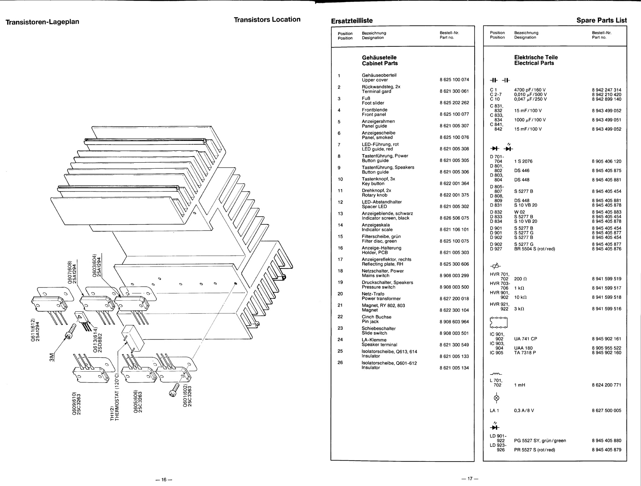
Blaupunkt-Gerate
erfullen
die
in
der
DIN
45
500
geforderten
Werte.
Die
Sicherheitsbestimmungen
der
internationalen
Sicherheitsnorm
IEC
65
werden
eingehalten
und
sind
bei
jeder
Reparatur
zu
beach-
ten.
Alle
Bauteile,
die
mit
einem
solchen
Symbol
A
gekenn-
zeichnet
sind,
mUssen
durch
Originalteile
ersetzt
werden.
Technische
Daten
Bezeichnung
NetzanschluB
Leistungsaufnahme
Nennausgangsleistung
20
Hz
-
20
kHz,
K
=
0,02%,
4
20
Hz
-
20
kHz,
K
=
0,008%,
8
©
1kHz,40
1kHz,80
1kHz,80
bei
max.
Ausgangsleistung
Musikausgangsleistung
Dampfungsfaktor
Anstiegszeit
,slew
rate
Klirrfaktor
1TW,8
2
Intermodulation
250/8000
Hz
Leistungsbreite
Frequenzgang
Gerausch-Spannungsabstand
Fremdspannungsabstand
Kanaltrennung
250
-
10000
Hz
Eingangsempfindlichkeit/Impedanz
Abmessungen
Breite
Hohe
Tiefe
Gewicht
Wert/value
220
V,
50
Hz
800
W
2x240
W
2x
220
W
2x270W
2x270W
100
90
V/pus
0,01%
0,008%
5
Hz
-
100
kHz;
+1/-1dB
5
Hz
-
100
kHz;
+0/-0,5
dB
115
dB
95
dB
60
dB
1,0
V/50
kQ
437
mm
191
mm
428
mm
ca.
22
kg
The
Biaupunkt
units
fulfil
the
values
required
by
DIN
45
500.
The
unit
conforms
to
the
security
regulations
set
by
the
International
Security
Standard
IEC
65
and
these
must
be
observed
when
reparing
the
set.
Allcomponents
marked
by
A
mustbe
replaced
by
original
parts.
Technical
Data
Designation
Mains
Voltage
Power
Consumption
Output
Power
at
full
power
20
Hz
-
20
kHz,
K
=
0,02%,
4
0
20
Hz
—
20
kHz,
K
=
0,008%,
8
0
1
kHz,
40
1
kHz,80
1
kHz,
8
0
Music
Power
Damping
Factor
Slew
Rate
Distortion
Factor
Tw,8O
Intermodulation
250/8000
Hz
Power
Bandwidth
Frequency
Response
S/N
Ratio
Unweighted
S/N
Ratio
Channel
Separation
Input
Sensitivity
/Impedance
Dimensions
Width
Heigth
Depth
250
-
10000
Hz
Weight
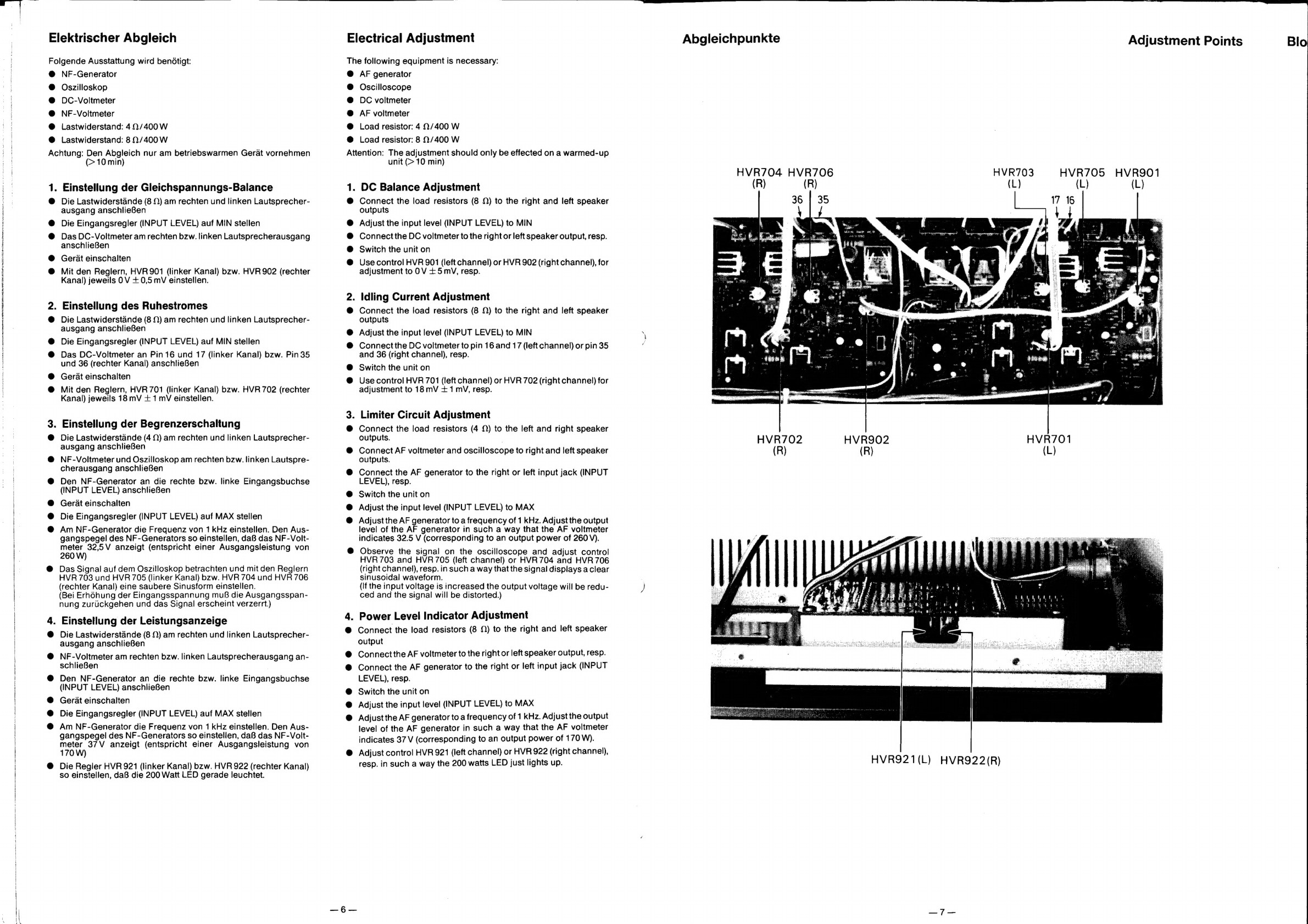
Funktionsbeschreibung
1.
Variable
Vorspannschaltung
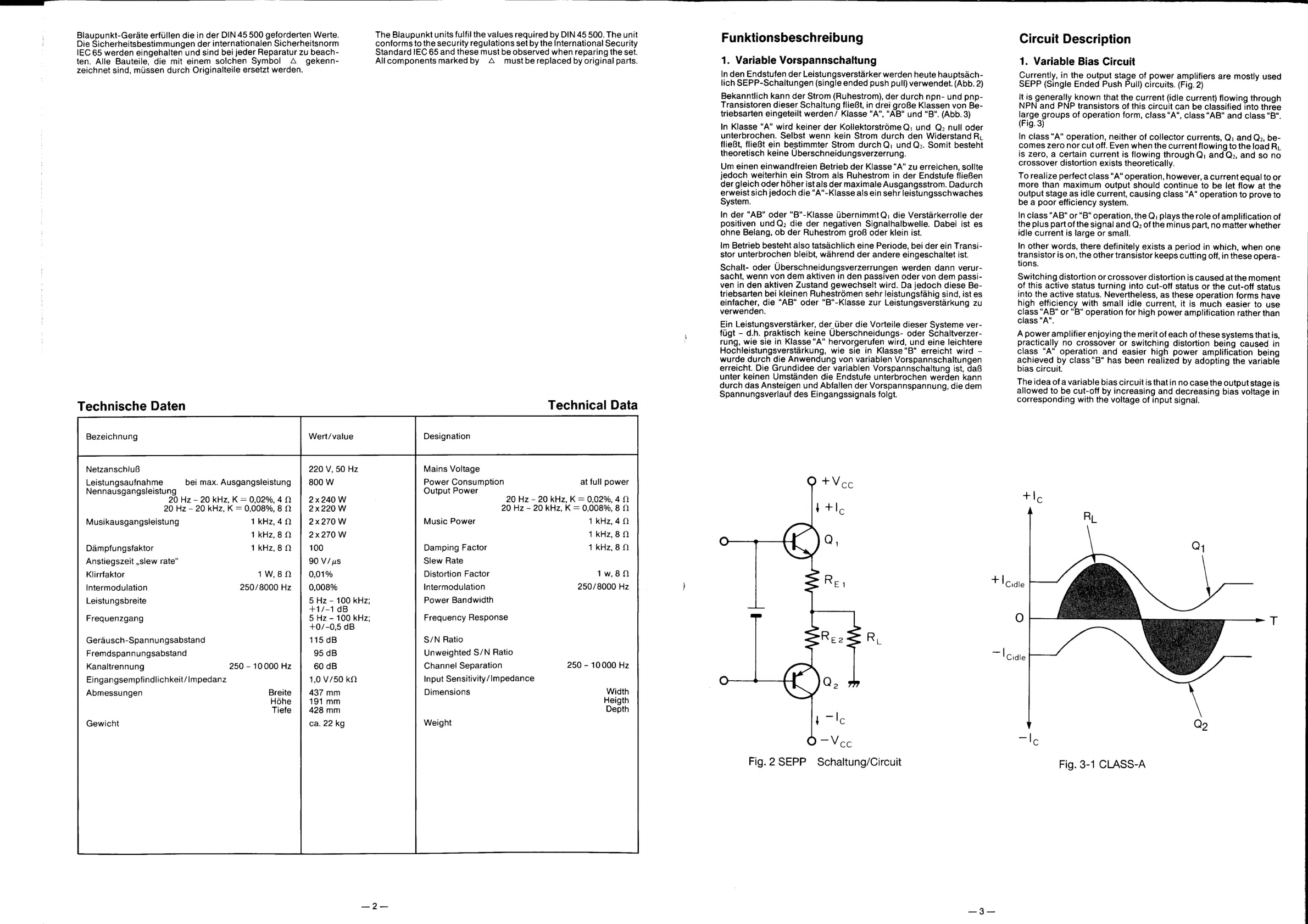
In
den
Endstufen
der
Leistungsverstarker
werden
heute
hauptsach-
lich
SEPP-Schaltungen
(single
ended
push
pull)
verwendet.
(Abb.
2)
Bekanntlich
kann
der
Strom
(Ruhestrom),
der
durch
npn-
und
pnp-
Transistoren
dieser
Schaltung
flieBt,
in
drei
groBe
Klassen
von
Be-
triebsarten
eingeteilt
werden/
Kiasse
“A*,
“AB“
und
“B“.
(Abb.
3)
In
Klasse
“A“
wird
keiner
der
Kollektorstrome
Q;
und
Q>
null
oder
unterbrochen.
Selbst
wenn
kein
Strom
durch
den
Widerstand
R;
flieBt,
flieBt
ein
bestimmter
Strom
durchQ,
und
Q2.
Somit
besteht
theoretisch
keine
Uberschneidungsverzerrung.
Um
einen
einwandfreien
Betrieb
der
Klasse
“A“
zu
erreichen,
sollte
jedoch
weiterhin
ein
Strom
als
Ruhestrom
in
der
Endstufe
flieBen
der
gleich
oder
hoher
ist
als
der
maximale
Ausgangsstrom.
Dadurch
erweist
sich
jedoch
die
“A“-Klasse
als
ein
sehr
leistungsschwaches
System.
In
der
“AB“
oder
“B“-Klasse
UbernimmtQ,
die
Verstarkerrolle
der
positiven
und
Q,
die
der
negativen
Signalhalbwelie.
Dabei
ist
es
ohne
Belang,
ob
der
Ruhestrom
groB
oder
klein
ist.
im
Betrieb
besteht
also
tatsachlich
eine
Periode,
bei
der
ein
Transi-
stor
unterbrochen
bleibt,
wahrend
der
andere
eingeschaltet
ist.
Schalt-
oder
Uberschneidungsverzerrungen
werden
dann
verur-
sacht,
wenn
von
dem
aktiven
in
den
passiven
oder
von
dem
passi-
ven
in
den
aktiven
Zustand
gewechselt
wird.
Da
jedoch
diese
Be-
triebsarten
bei
kleinen
Ruhestro6men
sehr
leistungsfahig
sind,
ist
es
einfacher,
die
“AB"
oder
“B"-Klasse
zur
Leistungsverstarkung
zu
verwenden.
Ein
Leistungsverstarker,
der
Uber
die
Vorteile
dieser
Systeme
ver-
fugt
-
d.h.
praktisch
keine
Uberschneidungs-
oder
Schaltverzer-
rung,
wie
sie
in
Klasse
“A*
hervorgerufen
wird,
und
eine
leichtere
Hochleistungsverstarkung,
wie
sie
in
Klasse“B“
erreicht
wird
-
wurde
durch
die
Anwendung
von
variablen
Vorspannschaltungen
erreicht.
Die
Grundidee
der
variablen
Vorspannschaltung
ist,
daB
unter
keinen
Umstanden
die
Endstufe
unterbrochen
werden
kann
durch
das
Ansteigen
und
Abfallen
der
Vorspannspannung,
die
dem
Spannungsverlauf
des
Eingangssignals
folgt.
—Vec
Fig.2
SEPP
Schaltung/Circuit
sg
loidle
—
lcidle
Circuit
Description
1.
Variable
Bias
Circuit
Currently,
in
the
output
stage
of
power
amplifiers
are
mostly
used
SEPP
(Single
Ended
Push
Pull)
circuits.
(Fig.
2)
It
is
generally
known
that
the
current
(idle
current)
flowing
through
NPN
and
PNP
transistors
of
this
circuit
can
be
classified
into
three
rate
groups
of
operation
form,
class
“A“,
class
“AB"
and
class
“B*“.
ig.
3)
In
class
“A*
operation,
neither
of
collector
currents,
Q;
and
Q:,
be-
comes
zero
nor
cut
off.
Even
when
the
current
flowing
to
the
load
Ri
is
zero,
a
certain
current
is
flowing
through
Q,
and
Q:,
and
so
no
crossover
distortion
exists
theoretically.
To
realize
perfect
class
“A“
operation,
however,
a
current
equal
to
or
more
than
maximum
output
should
continue
to
be
let
flow
at
the
output
stage
as
idle
current,
causing
class
“A“
operation
to
prove
to
be
a
poor
efficiency
system.
In
class
“AB*“
or
“B“
operation,
the
Q,
plays
the
role
of
amplification
of
the
pius
part
of
the
signal
and
Q:
of
the
minus
part,
no
matter
whether
idle
current
is
large
or
small.
In
other
words,
there
definitely
exists
a
period
in
which,
when
one
transistor
is
on,
the
other
transistor
keeps
cutting
off,
in
these
opera-
tions.
Switching
distortion
or
crossover
distortion
is
caused
at
the
moment
of
this
active
status
turning
into
cut-off
status
or
the
cut-off
status
into
the
active
status.
Nevertheless,
as
these
operation
forms
have
high
efficiency
with
small
idle
current,
it
is
much
easier
to
use
te
ne
or
“B"
operation
for
high
power
amplification
rather
than
class
“A“.
A
power
amplifier
enjoying
the
merit
of
each
of
these
systems
thatis,
practically
no
crossover
or
switching
distortion
being
caused
in
class
“A“
operation
and
easier
high
power
amplification
being
achieved
by
class
“B“
has
been
realized
by
adopting
the
variable
bias
Circuit.
The
idea
ofa
variable
bias
circuit
is
that
in
no
case
the
output
stage
is
allowed
to
be
cut-off
by
increasing
and
decreasing
bias
voltage
in
corresponding
with
the
voltage
of
input
signal.
tio
Fig.
3-1
CLASS-A