Elenco Electronics TCT-255K User guide

MULTI-NETWORK CABLE TESTER KIT
MODEL TCT-255K
Elenco Electronics, Inc.
Assembly and Instruction Manual
Copyright © 2001 Elenco Electronics, Inc. 753089

GENERAL DISCUSSION
You can see a block diagram of the TCT-255 in Figure 1 below.
The TCT-255 Cable Tester has five basic blocks:
1. Power Supply
It powers all of the circuits of the tester (not including the terminator). The power supply has a low battery
indicator (less than 7.5V) and a circuit to disconnect power 30 - 50 seconds after the last push on the
test switch.
2. Oscillator
Uses a 555 timer IC with two resistors and one capacitor. They control the free running frequency and
duty cycle.
3. Step Pulses with Counter
The outputs change by the positive pulses from the test button switch.
4. Switches and LED Indicator
It includes eight electronic switches for operating the indicators (16 LEDs).
5. Terminator
Connected to cable under test. Identifies the polarity signals.
Cable Tester TCT-200 Terminator LD-100
Figure 1
COUNTER SWITCHES
INPUT & OUTPUT
CONNECTORS
INPUT & OUTPUT
CONNECTORS
STEP PULSES
OSCILLATOR LED
INDICATOR
CIRCUIT
IDENTIFY
POLARITY
POWER
SUPPLY
-1-
The TCT-255 Cable Tester is a convenient instrument
for testing different unshielded wiring schemed
communication cable with RJ-11 and RJ-45
connectors and coax cable. This tester can be used
for testing cables before and/or after they are
installed. The tester offers easy operation by having
to push only one button.Testing status is indicated by
multiple LEDs and an auto power-off function
maximizes battery life.
The unique design of the TCT-255 allows you to
place the parts over their corresponding symbol in
the schematic drawing on the surface of the PC
board during assembly. This technique maximizes
the learning process while keeping the chances of
an assembly error at a minimum. It is very
important, however, that good soldering practices
are used to prevent bad connections.
The actual assembly is broken into SEVEN
SECTIONS. After each assembly, you will be
instructed to make certain tests and measurements
to prove that each section is functioning properly.
The theory for each section, or stage, should be
read before the test is started. This will provide the
student with an understanding of what that stage
has been designed to accomplish, and how it
actually works. If a test fails to produce the proper
results, a troubleshooting guide is provided to help
you correct the problem. For testing you need to
have only a voltmeter for measuring DC and AC.
INTRODUCTION

IDENTIFYING RESISTOR VALUES
Use the following information as a guide in properly identifying the value of resistors.
IDENTIFYING CAPACITOR VALUES
Capacitors will be identified by their capacitance value in pF (picofarads), nF (nanofarads), or mF (microfarads). Most
capacitors will have their actual value printed on them. Some capacitors may have their value printed in the following
manner. The maximum operating voltage may also be printed on the capacitor.
Second Digit
First Digit
Multiplier
Tolerance The letter M indicates a tolerance of +20%
The letter K indicates a tolerance of +10%
The letter J indicates a tolerance of +5%
FortheNo.01234589
Multiply By 1 10 100 1k 10k 100k .01 0.1
Multiplier
Note: The letter “R” may be used at times
to signify a decimal point; as in 3R3 = 3.3
BANDS
12 Multiplier Tolerance
103K
100
Maximum Working Voltage
The value is 10 x 1,000 = 10,000pF or .01mF 100V
-2-

-3-
CONSTRUCTION
Introduction
Assembly of your TCT-255 Multi-Network Cable Tester Kit will prove to be an exciting project
and give you much satisfaction and personal achievement. If you have experience in soldering
and wiring techniques, then you should have no problem with the assembly of this kit. Care
must be given to identifying the proper components and in good soldering habits. Above all,
take your time and follow these easy step-by-step instructions. Remember, “An ounce of
prevention is worth a pound of cure”. Avoid making mistakes and no problems will occur.
Safety Procedures
• Wear eye protection when soldering.
•
Locate soldering iron in an area where you do not have to go around it or reach over it.
• Do not hold solder in your mouth. Solder contains lead and is a toxic substance. Wash your
hands thoroughly after handling solder.
• Be sure that there is adequate ventilation present.
Assemble Components
In all of the following assembly steps, the components must be installed on the top side of the
PC board unless otherwise indicated. The top legend shows where each component goes.
The leads pass through the corresponding holes and the board is turned to solder the
component leads on the foil side. Solder immediately unless the pad is adjacent to another
hole which will interfere with the placement of the other component. Cut excessive leads with
a diagonal cutter. Then, place a check mark in the box provided next to each step to indicate
that the step is completed. Be sure to save the extra leads for use as jumper wires if needed.
Soldering
The most important factor in assembling your cable tester kit is good soldering techniques.
Using the proper soldering iron is of prime importance. A small pencil type soldering iron of
25 - 40 watts is recommended. The tip of the iron must be kept clean at all times and well
tinned. Many areas on the PC board are close together and care must be given not to form
solder shorts. Size and care of the tip will eliminate problems.
For a good soldering job, the areas being soldered must be heated sufficiently so that the
solder flows freely. Apply the solder simultaneously to the component lead and the component
pad on the PC board so that good solder flow will occur. Be sure that the lead extends through
the solder smoothly indicating a good solder joint. Use only rosin core solder of 63/37 or
60/40 alloy.
DO NOT USE ACID CORE SOLDER! Do not blob the solder over the lead because this can
result in a cold solder joint.
Heat Sinking
Electronic components such as transistors,
IC’s, and diodes can be damaged by the heat
during soldering. Heat sinking is a way of
reducing the heat on the components while
soldering. Dissipating the heat can be
achieved by using long nose pliers, an alligator
clip, or a special heat dissipating clip. The heat
sink should be held on the component lead
between the part and the solder joint.
Mount Part Bend Leads to Hold Part Solder and Cut Off Leads
Foil Side
Rx - 100W5% 1/4W Resistor
(brown-black-brown-gold)
Heat Sink (this can be ordered as part of Elenco’s Solder Ease
Kit Model SE-1).
Soldering Iron
Solder
Heat Sensitive
Component (Diode)
PC Board
Figure 6

-4-
What Good Soldering Looks Like
A good solder connection should be bright, shiny,
smooth, and uniformly flowed over all surfaces.
Soldering a PC board
1. Solder all components
from the copper foil side
only. Push the soldering
iron tip against both the
lead and the circuit board
foil.
2. Apply a small amount of
solder to the iron tip. This
allows the heat to leave
the iron and onto the foil.
Immediately apply solder
to the opposite side of the
connection, away from
the iron. Allow the heated
component and the circuit
foil to melt the solder.
3. Allow the solder to flow
around the connection.
Then, remove the solder
and the iron and let the
connection cool. The
solder should have flowed
smoothly and not lump
around the wire lead.
4.
Here is what a good
solder connection looks
like.
Types of Poor Soldering Connections
1. Insufficient heat - the
solder will not flow onto
the lead as shown.
2. Insufficient solder -
let the solder flow over
the connection until it is
covered. Use just
enough solder to cover
the connection.
3. Excessive solder -
could make
connections that you
did not intend to
between adjacent foil
areas or terminals.
4. Solder bridges - occur
when solder runs
between circuit paths
and creates a short
circuit. This is usually
caused by using too
much solder. To correct
this, simply drag your
soldering iron across
the solder bridge as
shown.
A poorly soldered joint can greatly affect small current flow in circuits and can cause equipment failure. You can damage
a PC board or a component with too much heat or cause a cold solder joint with insufficient heat. Sloppy soldering can
cause bridges between two adjacent foils preventing the circuit from functioning.
Solder Soldering Iron
Foil
Solder
Soldering Iron
Foil
Component Lead
Soldering Iron
Circuit Board
Foil
Rosin
Soldering iron positioned
incorrectly.
Solder
Gap
Component Lead
Solder
Soldering Iron
Drag
Foil
TROUBLESHOOTING
1. One of the most frequently occurring problems is poor
solder connections.
a) Tug slightly on all parts to make sure that they
are indeed soldered.
b) All solder connections should be shiny.
Resolder any that are not.
c) Solder should flow into a smooth puddle rather
than a round ball. Resolder any connection that
has formed into a ball.
d) Have any solder bridges formed? A solder
bridge may occur if you accidentally touch an
adjacent foil by using too much solder or by
dragging the soldering iron across adjacent foils.
Break the bridge with your soldering iron.

PARTS LIST - SECTION A
RESISTORS
Qty. Symbol Description Color Code Part #
2 R12, R17 1kW5% 1/4W brown-black-red-gold 141000
1 R16 5.6kW5% 1/4W green-blue-red-gold 145600
1 R15 12kW5% 1/4W brown-red-orange-gold 151200
1 R9 3.3MW5% 1/4W orange-orange-green-gold 173300
CAPACITORS
Qty. Symbol Value Description Part #
1 C2 22mF Electrolytic Radial 272244
SEMICONDUCTORS
Qty. Symbol Value Description Part #
1 D17 1N4001 Silicon Diode 314001
1*1N4736 Zener Diode 6.8V 1W 314736
1 D18 1N5235 Zener Diode 6.8V 0.5W 315235
2 Q2, Q3 2N3904 Transistor NPN 323904
1 Q1 2N3906 Transistor PNP 323906
1 D19 LED Red 350003
1 U4 40106 Integrated Circuit (IC) Hex Inverter 330106
MISCELLANEOUS
Qty. Symbol Description Part #
1 PC Board Tester TCT-200 517041
1 SW1 Switch Push Button DPDT 540203
1 Battery 9V 590009
1 Battery Snap 9V 590098
1 Spacer 624018
1 U4 Socket IC 14-pin 664014
1 Tubing #20 1/2” 890020
1 Solder 9ST4
* Packaged in a separate bag, used for testing only.
SECTION A
Power Supply
PARTS IDENTIFICATION
Integrated Circuit (IC)
-5-
Resistor DiodesElectrolytic Transistor LED
IC Socket 14-pin
PC Board (Tester)
Switch Push Button
Epoxy
Zener
Battery Snap Spacer
Tubing

Figure B
Mount the LED with the tubing and
plastic spacer to the PC board as
shown. Note the flat side of the
LED and the PC board marking.
ASSEMBLE THE FOLLOWING COMPONENTS TO THE PC BOARD
In all of the following steps the components must be installed on the top legend side of the PC board. The
board is turned to solder the component leads on the foil side.
R17 - 1kW5% 1/4W Resistor
(brown-black-red-gold)
(see Figure A)
D19 - LED Red
Tubing
Spacer
(see Figure B)
R9 - 3.3MW5% 1/4W Resistor
(orange-orange-green-gold)
(see Figure A)
Q2 - 2N3904 Transistor NPN
(see Figure C)
D17 - 1N4001 Diode (epoxy)
(see Figure D)
Q3 - 2N3904 Transistor NPN
(see Figure C)
U4 - 14-pin IC Socket
U4 - 40106 IC Hex Inverter
(see Figure E)
SW1 - Push Button Switch
(see Figure F)
R16 - 5.6kW5% 1/4W Resistor
(green-blue-red-gold)
(see Figure A)
C2 - 22mF Electrolytic
(see Figure G)
R15 - 12kW5% 1/4W Resistor
(brown-red-orange-gold)
(see Figure A)
R12 - 1kW5% 1/4W Resistor
(brown-black-red-gold)
(see Figure A)
D18 - 1N5235 Zener Diode 0.5W
(see Figure D)
Battery Snap
(see Figure H)
Q1 - 2N3906 Transistor PNP
(see Figure C)
Figure A
Mount the resistor
flat against the PC
board as shown.
Figure D
Diodes have polarity. Mount the
diodes in the direction marked on
the PC board as shown.
Polarity
Marking
Polarity
Marking
Epoxy
Zener
-6-
Figure F
IMPORTANT!!! Mount the push button
switch as shown. The circle MUST be
facing the other direction from the marking
“SW1” on the PC board.
Figure G
Electrolytic capacitors have polarity. Be sure
to mount them with the negative (--) lead
(marked on the side) in the correct hole.
Polarity
Marking
Flat Side Spacer
LED
Tubing
Figure C
Mount the
transistor to
the PC board
noting the flat
side.
Flat Side
Figure E
Insert the IC socket into the PC board with the
notch in the direction shown on the top
legend. Solder the IC socket into place.
Insert the IC into the socket with the notch in
the same direction as the notch on the socket.
Notch
Notch
Marking
Figure H
Mount the battery
snap as shown.
The black (--) lead
goes to --B and
the red (+) lead
goes to +B.
Circle
Red Lead
Black Lead
(--) (+)
1/8”

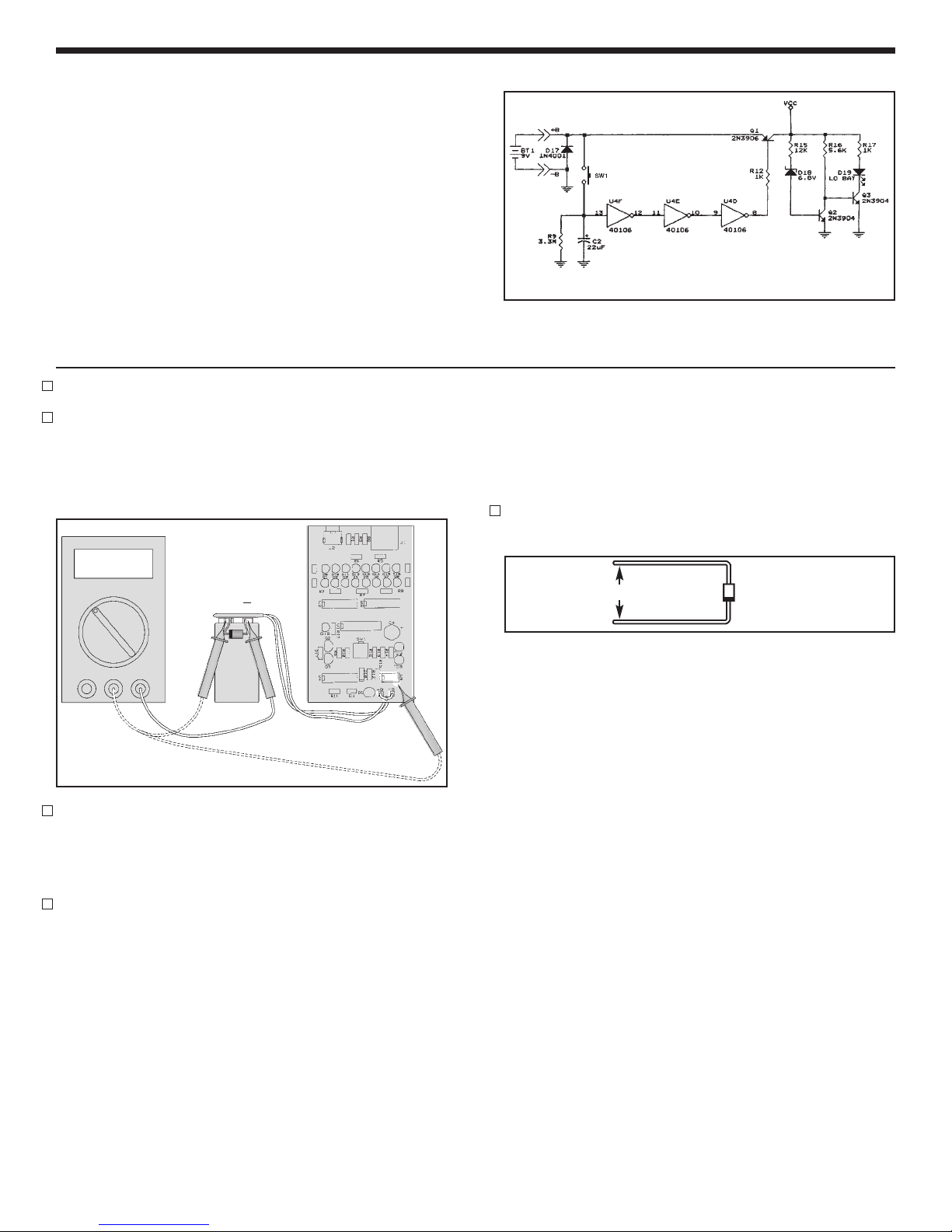
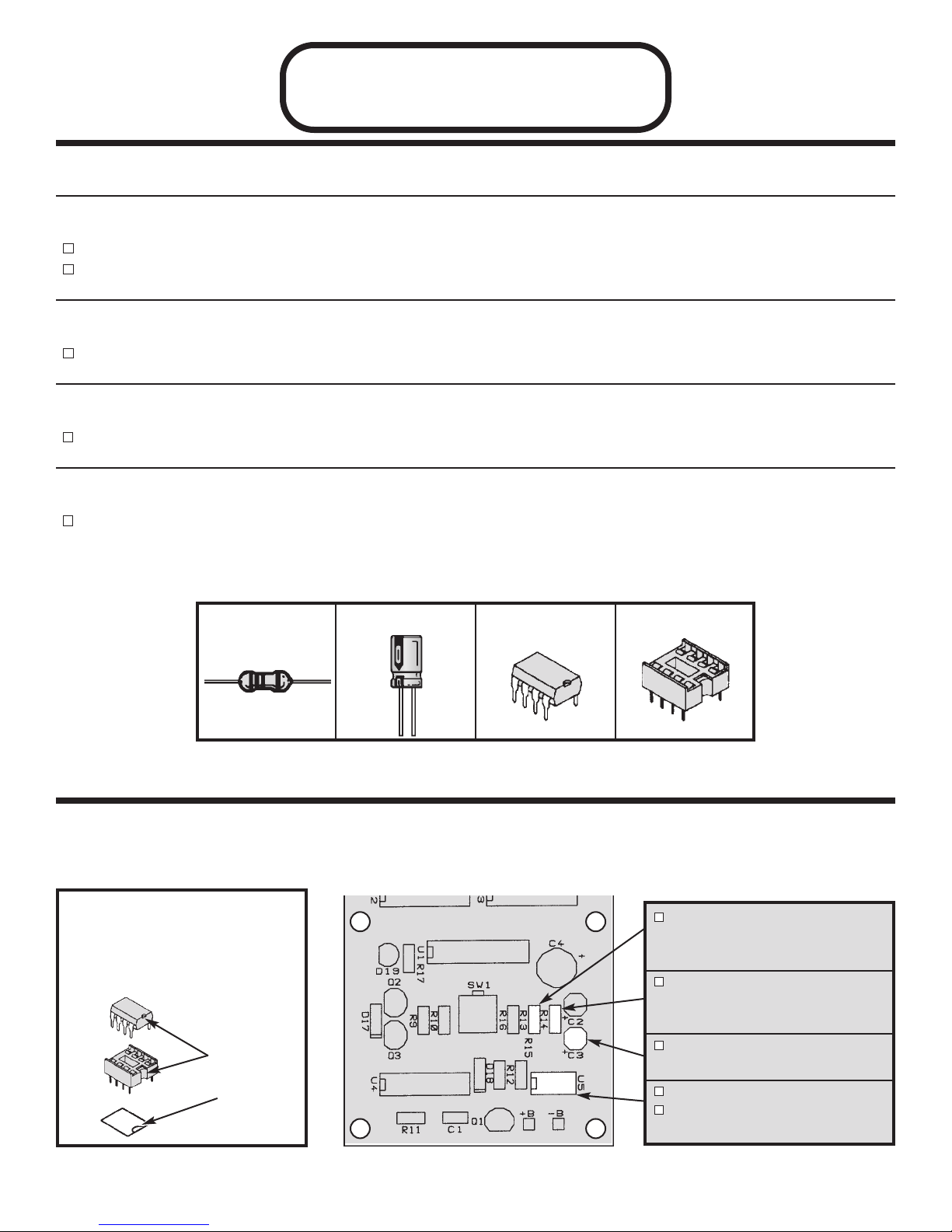
SECTION A - POWER SUPPLY
When the SW1 (test button) is pushed, capacitor C2
(see schematic diagram, Figure 1) is charged to the
battery voltage. Transistor Q1 turns on and all of the
circuits in the tester are powered. If you don’t push
SW1, capacitor C2 begins discharging. When the
voltage on C2 is less than 0.7V, transistor Q1 and
the power turn off after 30-50 seconds.
When the voltage of the battery is less than 7.5V,
transistors Q2 and Q3 turn on and LED D19 (Low
Battery) lights. The diode D17 protects the tester
from wrong polarity input voltage.
-7-
1. Connect the battery to the battery snap.
2. Set the voltmeter to read 20VDC and connect the
COM lead to the negative (--) side of the battery
and the V lead to the positive (+) side of the
battery as shown in Figure 2. The meter should
indicate 9-10VDC. Push switch SW1.
3.
Remove the V lead from the positive (+) side of the
battery and move to pad of pin 4 of IC U5. The
meter should indicate the same voltage, but after
30-50 seconds, the voltage should drop to 0V.
4. Push the switch SW1 again. The meter should
indicate the same voltage as in step 2. If not:
a) Check that the battery snap is connected
with the the right polarity as shown in the
assembly instructions.
b) Check that the transistor Q1 is 2N3906 and
mounted with the emitter, base and collector
leads as shown in the assembly instructions.
c) Check that R9, R12 and C2 are the correct
values.
d) Check that D17, D18, C2, U4 and SW1 are
installed as shown in the assembly
instructions.
5. Bend the zener diode 1N4736 (6.8V 1W, located
in a separate bag) as shown in Figure 3.
Push the switch SW1 again and short the battery
by the zener diode for 1-2 seconds (the side with
the band should be touching the “+” terminal of the
battery, see Figure 2). LED D19 (Lo Batt.) should
be lit. Remove the zener diode and the LED should
turn off. If not:
a) Check that the transistors Q2 and Q3 are
2N3904 and mounted as shown in the
assembly instructions.
b) Check zener diode D18 and LED D19. Be
sure that they are installed as shown in the
assembly instructions.
c) Check that resistors R15, R16 and R17 are
the correct values.
Remove the battery from the battery snap and
the leads from the tester.
TESTING
Figure 1
Figure 3
0.5” - 0.6”
VCOM
VDC +
9V
Figure 2
1
8

PARTS LIST - SECTION B
RESISTORS
Qty. Symbol Description Color Code Part #
1 R13 18kW5% 1/4W brown-gray-orange-gold 151800
1 R14 100kW5% 1/4W brown-black-yellow-gold 161000
CAPACITORS
Qty. Symbol Value Description Part #
1C3 1mF Electrolytic Radial 261047
SEMICONDUCTORS
Qty. Symbol Value Description Part #
1 U5 555 Integrated Circuit (IC) 555 Timer 330555
MISCELLANEOUS
Qty. Symbol Description Part #
1 U5 Socket IC 8-pin 664008
SECTION B
Oscillator
PARTS IDENTIFICATION
-8-
Resistor
Integrated Circuit (IC)
Electrolytic IC Socket 8-pin
Figure I
Insert the IC socket into the PC board with the
notch in the direction shown on the top
legend. Solder the IC socket into place.
Insert the IC into the socket with the notch in
the same direction as the notch on the socket.
ASSEMBLE THE FOLLOWING COMPONENTS TO THE PC BOARD
In all of the following steps the components must be installed on the top legend side of the PC board. The
board is turned to solder the component leads on the foil side.
R13 - 18kW5% 1/4W Resistor
(brown-gray-orange-gold)
(see Figure A)
R14 - 100kW5% 1/4W Resistor
(brown-black-yellow-gold)
(see Figure A)
C3 - 1mF Electrolytic Radial
(see Figure G)
U5 - 8-pin IC Socket
U5 - 555 IC Timer
(see Figure I)
Notch
Notch
Marking

1. Connect the battery to the battery snap.
2. Set the voltmeter to read 20VAC and connect the
COM lead to the negative (–) side of the battery
and the V lead to pad of pin 8 of IC U3 as shown
in Figure 5. The meter should indicate 0V. Push
switch SW1. The meter should indicate 3-5VAC.
If not:
a) Check U5 and C3 to be sure that they are
installed as shown in the assembly
instructions.
b) Check R13 and R14 are the correct values.
Remove the battery from the battery snap and
the leads from the tester.
-9-
SECTION B - OSCILLATOR
The oscillator section consists of a 555 timing
circuit, resistors R13, R14, and capacitor C3. The
555 IC is configured as an astable or free-running
oscillator. The values of the resistor R14 and
capacitor C3 set the output frequency at 8Hz. The
IC will produce a continuous 8Hz square wave from
pin 3 as long as it is powered.
TESTING
Figure 4
To Switches
Figure 5
VCOM
VAC +
9V
1
14

Figure J
Insert the IC socket into the PC board with the
notch in the direction shown on the top
legend. Solder the IC socket into place.
Insert the IC into the socket with the notch in
the same direction as the notch on the socket.
-10-
PARTS LIST - SECTION C
RESISTORS
Qty. Symbol Description Color Code Part #
1 R11 680kW5% 1/4W blue-gray-yellow-gold 166800
1 R10 1.2MW5% 1/4W brown-red-green-gold 171200
CAPACITORS
Qty. Symbol Value Description Part #
1 C1 .001mF Discap (102 or .001) 231035
SEMICONDUCTORS
Qty. Symbol Value Description Part #
1 U1 4017 Integrated Circuit (IC) Decade Counter 334017
MISCELLANEOUS
Qty. Symbol Description Part #
1 U1 Socket IC 16-pin 664016
SECTION C
Step Pulses with Counter
PARTS IDENTIFICATION
Resistor
Integrated Circuit (IC)
Capacitor IC Socket 16-pin
102
ASSEMBLE THE FOLLOWING COMPONENTS TO THE PC BOARD
In all of the following steps the components must be installed on the top legend side of the PC board. The
board is turned to solder the component leads on the foil side.
U1 - 16-pin IC Socket
U1 - 4017 IC Decade Counter
(see Figure J)
R10 - 1.2MW5% 1/4W Resistor
(brown-red-green-gold)
(see Figure A)
R11 - 680kW5% 1/4W Resistor
(blue-gray-yellow-gold)
(see Figure A)
C1 - .001mF Discap
(102 or .001)
Notch
Notch
Marking

1. Connect the battery to the battery snap.
2. Set the voltmeter to read 20VDC and connect the
COM lead to the negative (–) side of the battery
and the V lead to pin 3 of IC U1 as shown in
Figure 7.
3.
Push switch SW1 until the voltmeter indicates
9-10VDC.
4. Move the V lead of the voltmeter to pin 2. The
voltmeter should indicate 0V. Push SW1 again.
The voltmeter should indicate 8-9VDC.
In the same manner, test the outputs of the
counter (pins 4, 7, 10, 1, 5, and 6).
If the test results are not satisfactory, then:
a) Check U1. Be sure that it is installed as
shown in the assembly instructions.
Remove the battery from the battery snap and
the leads from the tester.
SECTION C - STEP PULSES WITH COUNTER
In this section, a 4017 counter IC and a 40106
inverter IC are used to control eight electronic
switches. A short positive pulse must be generated
and applied to the clock input of the 4017 IC
whenever switch SW1 is depressed. This is done by
wiring three inverters in series. When switch SW1 is
depressed, the voltage at pin 1 of the 40106 is
pulled to ground. This low condition is then inverted
three times to produce a positive pulse to the CLK
pin of the 4017.
The 4017 IC is a five-stage Johnson decade
counter. The IC has 10 outputs, but only one output
will be driven high at any given time, the other nine
will be low. For each pulse at the clock (CLK) input,
the output will move one position. In this design,
only eight outputs are used, the ninth output is wired
to the reset (RST) pin. When the reset pin goes
high, it sets the Q0 output high again. The clock
enable (ENA) pin is tied to ground, so every clock
pulse will move the output.
TESTING
Figure 6
-11-
To Switches
}
1
16
VDC
9V
+
VCOM
Figure 7

-12-
PARTS LIST - SECTION D
RESISTORS
Qty. Symbol Description Color Code Part #
8 R1-R8 200W5% 1/4W red-black-brown-gold 132000
CAPACITORS
Qty. Symbol Value Description Part #
1 C4 470mF 16V Electrolytic Radial 284744
SEMICONDUCTORS
Qty. Symbol Value Description Part #
16 D1-D16 LED Red 350003
2 U2, U3 74HC4066 Integrated Circuit (IC) Quad Analog Switch 394066
MISCELLANEOUS
Qty. Symbol Description Part #
1 J2 F-Connector 590500
1 J1 Modular Jack RJ-45 621028
2 Spacer 624006
2 U2, U3 IC Socket 14-pin 664014
SECTION D
Switches and LED Indicator
PARTS IDENTIFICATION
Resistor
Integrated Circuit (IC)
Electrolytic IC Socket 14-pin
F-Connector Modular Jack LED Spacer

ASSEMBLE THE FOLLOWING COMPONENTS TO THE PC BOARD
In all of the following steps the components must be installed on the top legend side of the PC board. The
board is turned to solder the component leads on the foil side.
R6 - 200W5% 1/4W Resistor
(red-black-brown-gold)
(see Figure A)
R3 - 200W5% 1/4W Resistor
(red-black-brown-gold)
(see Figure A)
R1 - 200W5% 1/4W Resistor
(red-black-brown-gold)
(see Figure A)
J2 - F-Connector
(see Figure K)
R4 - 200W5% 1/4W Resistor
(red-black-brown-gold)
(see Figure A)
R2 - 200W5% 1/4W Resistor
(red-black-brown-gold)
(see Figure A)
R7 - 200W5% 1/4W Resistor
(red-black-brown-gold)
(see Figure A)
U2 - 14-pin IC Socket
U2 - 74HC4066 IC
(see Figure E)
J1 - Modular Jack RJ-45
(see Figure L)
R5 - 200W5% 1/4W Resistor
(red-black-brown-gold)
(see Figure A)
R8 - 200W5% 1/4W Resistor
(red-black-brown-gold)
(see Figure A)
U3 - 14-pin IC Socket
U3 - 74HC4066 IC
(see Figure E)
C4 - 470mF Electrolytic Radial
(see Figure G)
-13-
Figure K
Mount and solder the F-connector to the PC board in the
location shown. Note: The connector must be soldered
in straight.
Figure L
Mount and solder the modular jack to the PC board as
shown.

-14-
ASSEMBLE THE FOLLOWING COMPONENTS TO THE PC BOARD (cont.)
Spacer
(see Figure M)
D9 - LED
D10 - LED
D11 - LED
D12 - LED
D13 - LED
D14 - LED
D15 - LED
D16 - LED
(see Figure N)
Figure M
Mount the spacer to the PC board as shown.
Figure N
Mount the LEDs onto the spacer as shown. Note the flat
side of the LED in relation to the marking on the PC
board. Solder and cut off the excess leads.
Spacer
(see Figure M)
D1 - LED
D2 - LED
D3 - LED
D4 - LED
D5 - LED
D6 - LED
D7 - LED
D8 - LED
(see Figure N)

1. Connect the battery to the battery snap.
2. Push the switch SW1. Two vertical LEDs should
be blinking at a frequency of approximately 8Hz.
3. Test the other pairs of LEDs by pushing switch
SW1. For every step, there should be only two
vertical blinking LEDs. If not, then:
a) Check U2, U3, C4 and diodes D1-D16. Be
sure that they are installed as shown in the
assembly instructions.
b) Check that the resistors R1-R8 installed are
the correct values.
c) Check the soldering on the modular jack and
F-connector.
TESTING
Figure 10
SECTION D - SWITCHES AND LED INDICATOR
In this section, two quad analog switches
(74HC4066) and 16 LEDs are used to indicate
which pins are being tested and the type of cable.
Figure 8 shows the logic diagram for each switch.
Each switch contains an input, output and a control
pin. The inputs are connected to the oscillator
section and the outputs to two LEDs and connector.
The control pins connect to the outputs of the 4017
IC (see Figure 10).
When switch A is closed, capacitor C charges and
discharges at the oscillator frequency. This causes
LEDs D1 and D2 to blink at the same rate (see
Figure 9a).
Connecting a straight cable, LED D3 will light only
during the charging cycle. The diode in the
terminator only allows the current flow in one
direction (see Figure 9b).
Connecting a cross-pinning cable, LED D4 will light
only during the discharging cycle (see Figure 9c).
Figure 8
Without Terminator
Figure 9a
ON/OFF Control
Analog
Input/Output
Analog
Output/Input
-15-
{
From
Counter
From Oscillator
Charge
Discharge
Straight Cable
Figure 9b
Cross-Pinning Cable
Figure 9c
A
B
A
B
A
B

-16-
PARTS LIST - SECTION E
SEMICONDUCTORS
Qty Symbol Value Description Part #
4 D1-D4 1N4148 Diode 314148
MISCELLANEOUS
Qty Symbol Description Part #
1 PC Board Terminator LD-100 510005
1 J2 F-Connector 590500
1 J1 Modular Jack RJ-45 621028
SECTION E
Terminator
PARTS IDENTIFICATION
F-Connector Modular Jack Diode PC Board
ASSEMBLE THE FOLLOWING COMPONENTS TO THE PC BOARD
In all of the following steps the components must be installed on the top legend side of the PC board. The
board is turned to solder the component leads on the foil side.
D4 - 1N4148 Diode
D3 - 1N4148 Diode
D2 - 1N4148 Diode
D1 - 1N4148 Diode
(see Figure D)
Note: R1 is not used.
Modular Jack (RJ-45)
(see Figure L)
J2 - F-Connector
Note: The connector must be
soldered in straight.
(see Figure K)
IMPORTANT: Cut off the
excess leads after soldering the
F-Connector to the PC board.

SECTION E - TERMINATOR
The terminator uses four diodes to identify the
polarity of the input signals. The diodes are placed
in series with wires 1-8, 2-7, 3-6, and 4-5 (see
Figure 11).
Figure 11
PARTS LIST - SECTION F
MISCELLANEOUS
Qty. Symbol Description Part #
4 Plug RJ-45 621032
2’ Cable Flat 8 Wires 870984
SECTION F
Assemble Telecom Cables
PARTS IDENTIFICATION
Plug RJ-45
8 Wire Flat Cable
-17-

-18-
ASSEMBLE THE TELECOM CABLES
For testing and troubleshooting the tester, you need to assemble straight and cross-pinning cables.
For cutting, stripping, and crimping, use a standard tool for RJ-45 plugs (flat cable).
Elenco Electronics has modular crimping tools Models ST-500 and HT-568.
Cut the 2’ telecom cable in half (see Figure 12).
Using the instructions for your tool, make two
cables (straight and cross-pinning) as shown in
Figures 13 - 15. Make sure that you make a clean
cut on the cable.
Figure 12 Cutting Figure 13 Stripping
Figure 15 Crimping
Figure 14
(BL) 1
(OR)2
(BK) 3
(R) 4
(G) 5
(Y) 6
(BN) 7
(S) 8
1
2
3
4
5
6
7
8
(BL) 1
(OR)2
(BK) 3
(R) 4
(G) 5
(Y) 6
(BN) 7
(S) 8
1
2
3
4
5
6
7
8
Straight Cable
Cross-Pinning Cable
Note the orientation of the
RJ-45 plug for each cable.

-19-
PARTS LIST - SECTION G
MISCELLANEOUS
Qty. Symbol Description Part #
2 F to BNC Adapter 596020
1 Button Cap 622006
1 Case Top Tester 623114
1*Case Top Terminator 623115
1 Case Bottom Tester 623211
1*Case Bottom Terminator 623212
1 Cover Battery 623401
1 Velcro Hook and Loop Set 628002
2 Screw #4 5/16” AB Phillips Pan Head 642442
4 Screw 3 x 12mm Thread Cutting Phillips Flat Head 643104
1 Screw M3 x 10mm Machine Phillips Flat Head 643105
1*Screw 2.6 x 10mm Thread Cutting Phillips Flat Head 643107
1*Label Terminator 727050
1 Label Tester 727051
* Used for the assembly of the terminator.
SECTION G
Final Test and Assembly
PARTS IDENTIFICATION
Button Cap Case Top Terminator
Case Top Tester Case Bottom Tester
Case Bottom Terminator Cover Battery
Velcro Hook & Loop Set Screws (actual size) Label Tester Label Terminator
#4 5/16” AB Phillips
Pan Head
3 x 12mm Thread Cutting
Phillips Flat Head
2.6 x 10mm Thread
Cutting Phillips Flat Head
Hook Loop
F to BNC
Adapter
M3 x 10mm Machine
Phillips Flat Head
Table of contents
Other Elenco Electronics Network Cables manuals
Popular Network Cables manuals by other brands

ADInstruments
ADInstruments AD8108 Instrument manual

Tripp Lite
Tripp Lite N002-007-WH Specification sheet

Tripp Lite
Tripp Lite N201-025-YW Specification sheet

Tripp Lite
Tripp Lite N002-007-BK Specification sheet

Tripp Lite
Tripp Lite N312-03M Specification sheet

Tripp Lite
Tripp Lite N201-025-BK Specifications