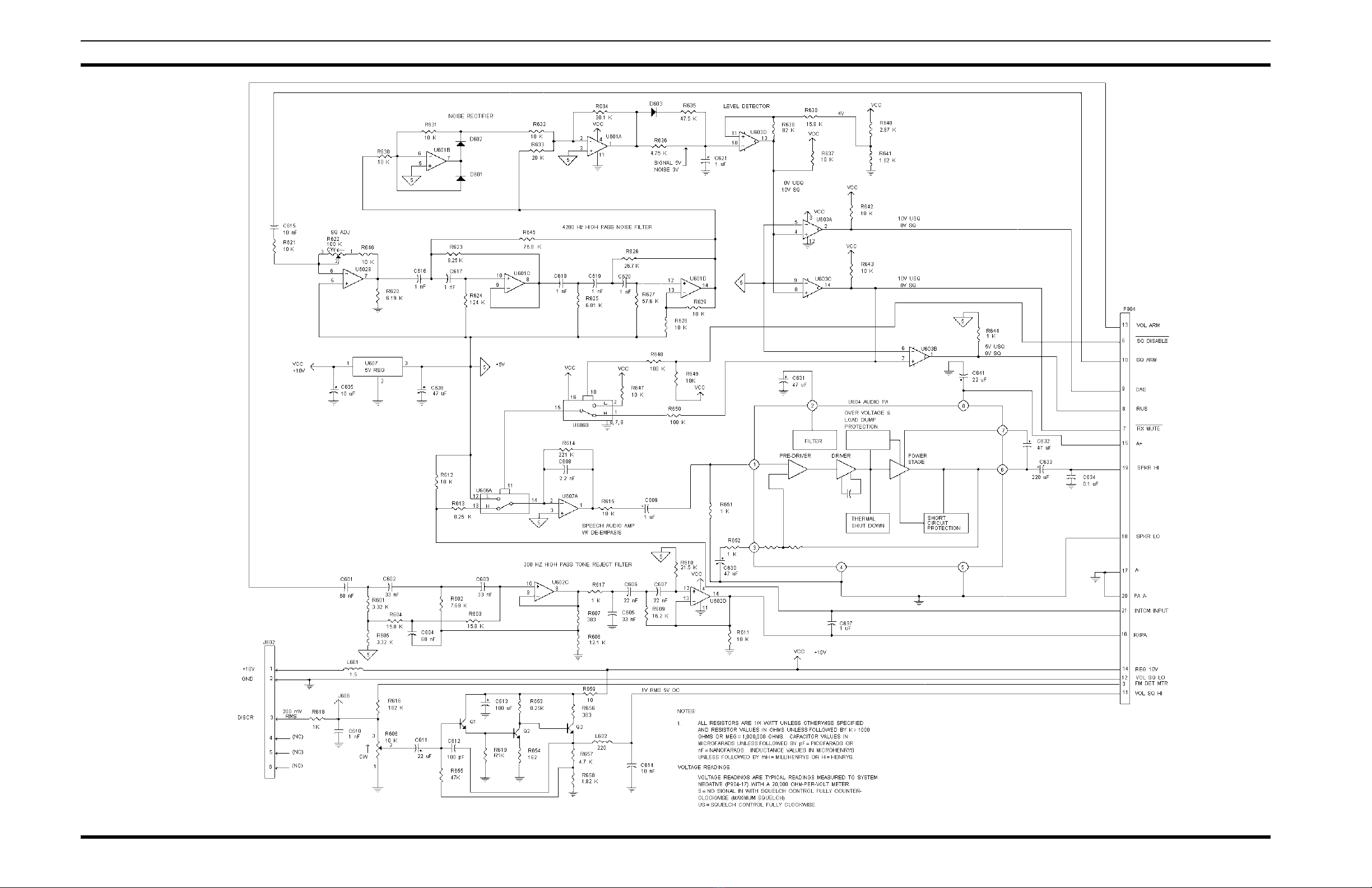
Pin 2 of U606-10 is connected to the system boardthrough
P904-6 (SQ DISABLE) so that the receiver audio stages can
be activated for an alert tone output whenever the Carrier
Controlled Timer or other options are used.
Squelch ICs
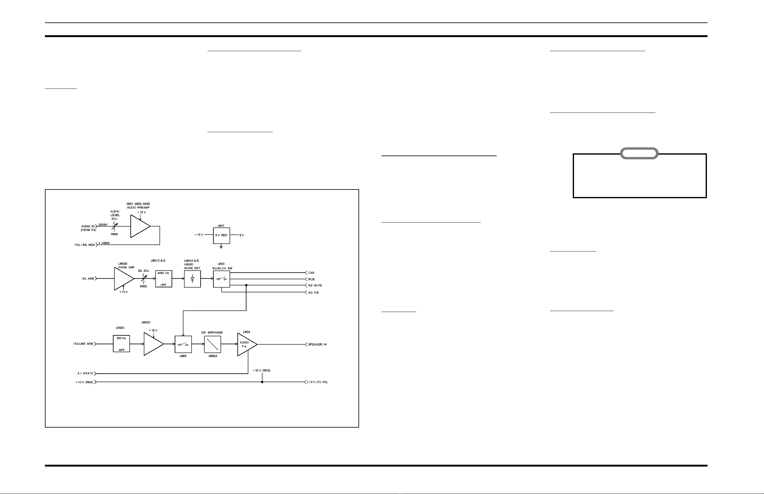
The receiver squelch circuit consists of noise amplifier
U602B, active noise filter U601C and U601D, noise rectifier
U601B, DC amp U601A, and level detector U603D. In addi-
tion, the squelch circuit contains the Receiver Unsquelched
Sensor (RUS) switch U603B, Carrier Activity Sensor (CAS)
switch U603A, and the RX MUTE switch U603C. The RX
MUTE switch controls the audio path to audio IC U604
through U606.
Noise Amp, Filter & Level Detector
Noise from the limiter/detector at P904-10 is coupled to
the noise amplifier U602B through the SQUELCH control,
andthenappliedtothe activenoisefilter(U601CandU601D).
The active filter provides the gain and selectivity necessary to
distinguish between noise and audio. The filter output at
U601D-14 drives the level detector circuit to provide the
squelch switching functions. Potentiometer R622 adjusts the
noise level for the proper squelch operation.
SQUELCH SWITCHES
Level detector U603D controls two of the switched
squelch outputs. The first output controls the RX MUTE
switch (U603C), and the second output controls the CAS
switch (U603A). The RUS switch (U603B) is also controlled
by the RX MUTE signal.
The squelch input to the level detector is at U603D-10.
U603D-11isreferencedto4VoltsfromvoltagedividerR640and
R641. When the receiver is squelched, the input at U603D-10 is
near 3 Volts, and the output at pin 13 is approximately 10 Volts.
This keeps the output of receiver audio stages turned off, muting
the audio. The level detector output is connected to its input
through R639, providing a hysteresis loop in the squelch circuit
to prevent squelch closing on weak signals.
When the receiver is quieted by an on-frequency signal
(receiver unsquelches),thevoltageatU603D-10risesto approxi-
mately 5 Volts DC, and the output at pin 14 drops to near 0 volts.
This turns on the audio stages and sound is heard at the speaker.
RUS Switch (Receiver Unsquelched Sensor)
When the receiver is unsquelched, the output of the level
detector(U603D-13)goeslow.ThelowturnsoffU603C,causing
U603B-1 to go high (approximately 10 Vdc), turning on RUS
switch U603B. The RUS output at U603B-1 is also connected
to the system board through P904-8 for use in special applica-
tions.
CAS Switch (Carrier Activity Sensor)
Leveldetector U603Dalso drivesCAS switch U603A.When
the receiver unsquelches, the voltage at U603A-2 rises to ap-
proximately 10 volts. This voltage is connected to the system
board through P904-9 where it is used to activated such options
as the Channel Busy light, Carrier Control Timer, and Carrier
Operated Relay.
MAINTENANCE
SERVICING
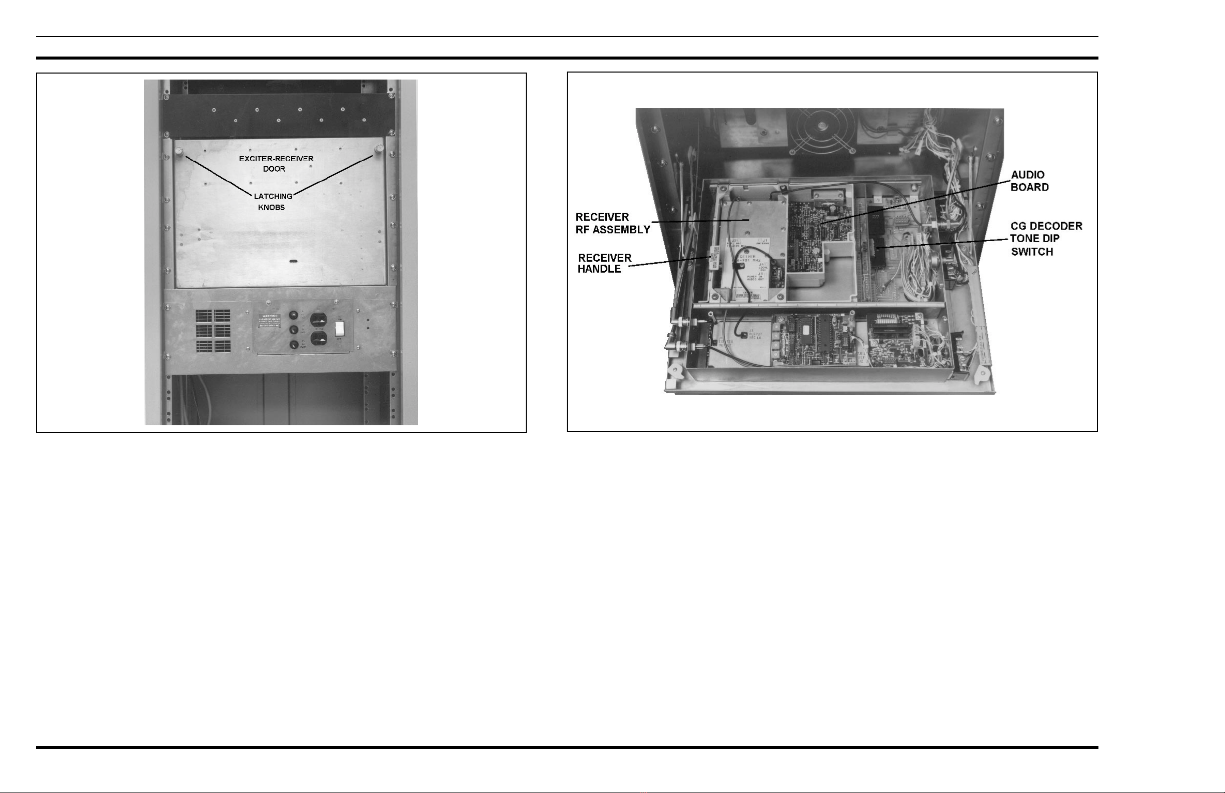
To gain access to the receiver for servicing:
To service the receiver from the top:
1. Turn the two latching knobs shown in Figure 3 counter-
clockwise to unlatch the exciter/receiver door.
2. Swing the exciter/receiver door housing down as shown
in Figure 4 and remove the top cover (exciter/receiver
door shown with cover removed).
To service the receiver from the bottom:
1. Turn the two latching knobs shown in Figure 3 counter-
clockwise to unlatch the exciter/receiver door housing
and swing the housing down as shown.
2. Remove the top cover. Then, grasp the receiver handle
shown in Figure 4 and swing the housingup for accessto
the bottom of the receiver.
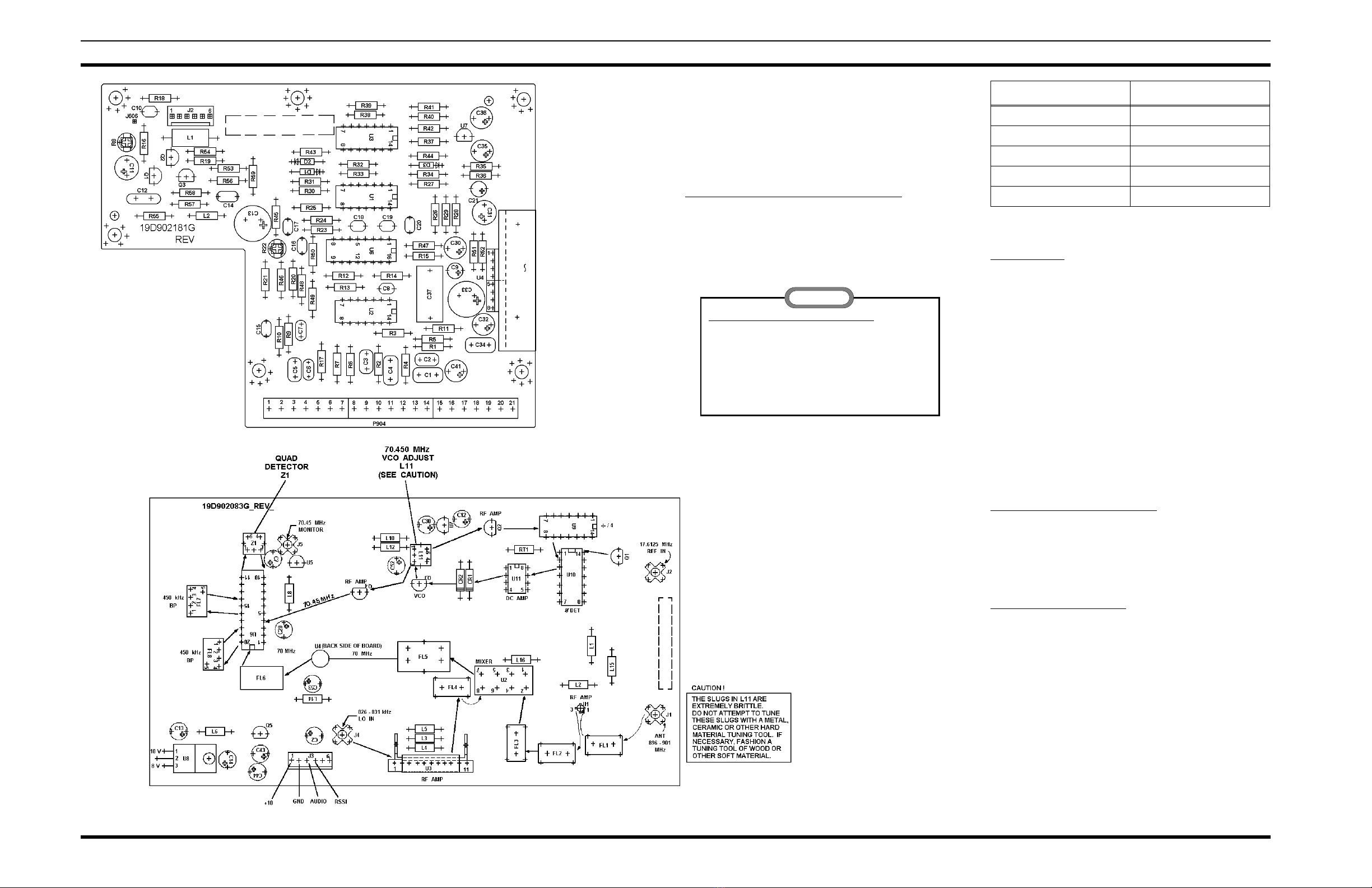
ADJUSTMENTS
The 900 MHz conventional receiver has no adjustments for
"peaking" up receiver performance. If some adjustment is re-
quired as a result of component replacement or other mainte-
nance, refer to the Adjustment Procedure contained in this Main-
tenance Manual.
TROUBLESHOOTING
Both the Schematic and Outline diagrams contain trou-
bleshooting information to assist in servicing the receiver. This
service information includes voltage and gain readings, power
levels and signal flowinformation.Referto these diagramswhen
troubleshooting the receiver (see Table of Contents).
Disconnect the two RF cables connecting the re-
ceiver and exciter, and remove the cable retaining
screw before raising the receiver housing as di-
rected in Step 2.
CAUTION
Figure 2 - Audio Board Block Diagram
LBI-38310
3