ESMT F25L02PA Series User manual

ESMT
F25L02PA (2F)
Operation Temperature Condition -40
°
C~85
°
C
Elite Semiconductor Memory Technology Inc.
Publication Date: Jan. 2012
Revision:
1.0
1/32
Flash
3V Only 2 Mbit Serial Flash Memory
with Dual Output
FEATURES
Single supply voltage 2.3~3.6V
Standard, Dual SPI
Speed
- Read max frequency: 33MHz
- Fast Read max frequency: 50MHz; 86MHz; 100MHz
- Fast Read Dual max frequency: 50MHz / 86MHz
(100MHz / 172MHz equivalent Dual SPI)
Low power consumption
- Active current: 20 mA
- Standby current: 25
µ
A
- Deep Power Down current: 10
µ
A
Reliability
- 100,000 typical program/erase cycles
- 20 years Data Retention
Program
- Page programming time: 0.7 ms (typical)
Erase
- Chip erase time 0.5 sec (typical)
- Block erase time 0.15 sec (typical)
- Sector erase time 30 ms (typical)
Page Programming
- 256 byte per programmable page
SPI Serial Interface
- SPI Compatible: Mode 0 and Mode 3
End of program or erase detection
Write Protect (
WP )
Hold Pin ( HOLD )
All Pb-free products are RoHS-Compliant
ORDERING INFORMATION
Product ID Speed
Package Comments
F25L02PA -50PIG2F 50MHz
F25L02PA -86PIG2F 86MHz
F25L02PA -100PIG2F 100MHz
8-lead
SOIC 150 mil
Pb-free
F25L02PA -50PAIG2F 50MHz
F25L02PA -86PAIG2F 86MHz
F25L02PA -100PAIG2F
100MHz
8-lead
SOIC 200 mil
Pb-free
F25L02PA -50HIG2F 50MHz
F25L02PA -86HIG2F 86MHz
F25L02PA -100HIG2F 100MHz
8-contact
WSON 6x5 mm
Pb-free
GENERAL DESCRIPTION
The F25L02PA is a 2Megabit, 3V only CMOS Serial Flash
memory device. The device supports the standard Serial
Peripheral Interface (SPI), and a Dual SPI. ESMT’s memory
devices reliably store memory data even after 100,000
programming and erase cycles.
The memory array can be organized into 1,024 programmable
pages of 256 byte each. 1 to 256 byte can be programmed at a
time with the Page Program instruction.
The device features sector erase architecture. The memory array
is divided into 64 uniform sectors with 4K byte each; 4 uniform
blocks with 64K byte each. Sectors can be erased individually
without affecting the data in other sectors. Blocks can be erased
individually without affecting the data in other blocks. Whole chip
erase capabilities provide the flexibility to revise the data in the
device. The device has Sector, Block or Chip Erase but no page
erase.
The sector protect/unprotect feature disables both program and
erase operations in any combination of the sectors of the
memory.
ESMT
F25L02PA (2F)
Operation Temperature Condition -40
°
C~85
°
C
Elite Semiconductor Memory Technology Inc.
Publication Date: Jan. 2012
Revision:
1.0
2/32
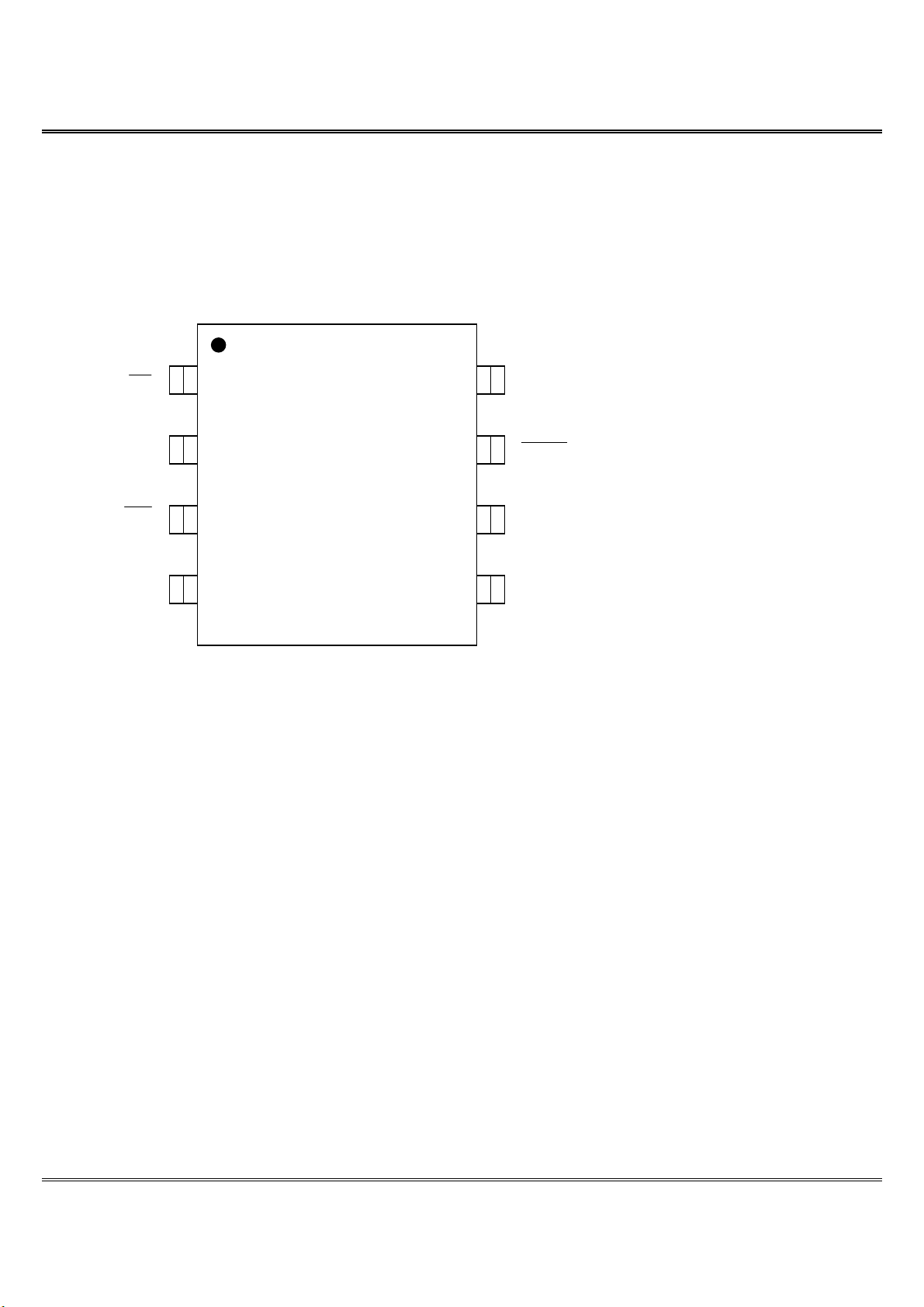
PIN CONFIGURATIONS
8- Lead SOIC
(SOIC 8L, 150mil Body, 1.27mm Pin Pitch)
(SOIC 8L, 208mil Body, 1.27mm Pin Pitch)
1 8
2 7
3 6
4 5
VDD
HOLD
SCK
SI
CE
SO
WP
VSS
ESMT
F25L02PA (2F)
Operation Temperature Condition -40
°
C~85
°
C
Elite Semiconductor Memory Technology Inc.
Publication Date: Jan. 2012
Revision:
1.0
3/32
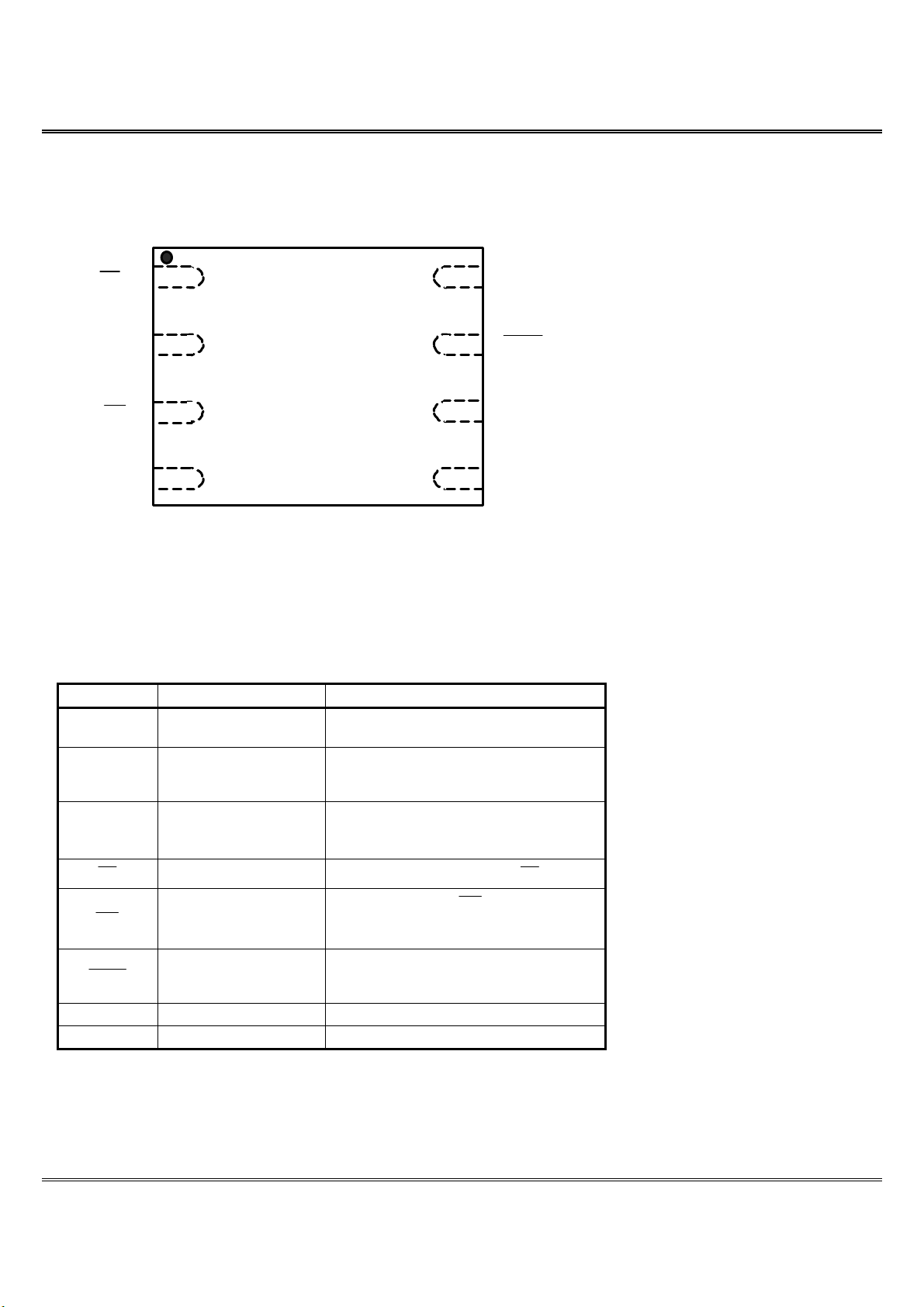
8- Contact WSON
(WSON 8C, 6mmX5mm Body, 1.27mm Contact Pitch)
PIN DESCRIPTION
Symbol Pin Name Functions
SCK Serial Clock To provide the timing for serial input and
output operations
SI Serial Data Input
To transfer commands, addresses or data
serially into the device.
Data is latched on the rising edge of SCK.
SO Serial Data Output
To transfer data serially out of the device.
Data is shifted out on the falling edge of
SCK.
CE Chip Enable To activate the device when CE is low.
WP Write Protect
The Write Protect ( WP ) pin is used to
enable/disable BPL bit in the status
register.
HOLD Hold
To temporality stop serial communication
with SPI flash memory without resetting
the device.
VDD Power Supply To provide power.
VSS Ground
1
2
3
4
8
7
6
5
CE
SO
WP
VSS
VDD
HOLD
SCK
SI
ESMT
F25L02PA (2F)
Operation Temperature Condition -40
°
C~85
°
C
Elite Semiconductor Memory Technology Inc.
Publication Date: Jan. 2012
Revision:
1.0
4/32
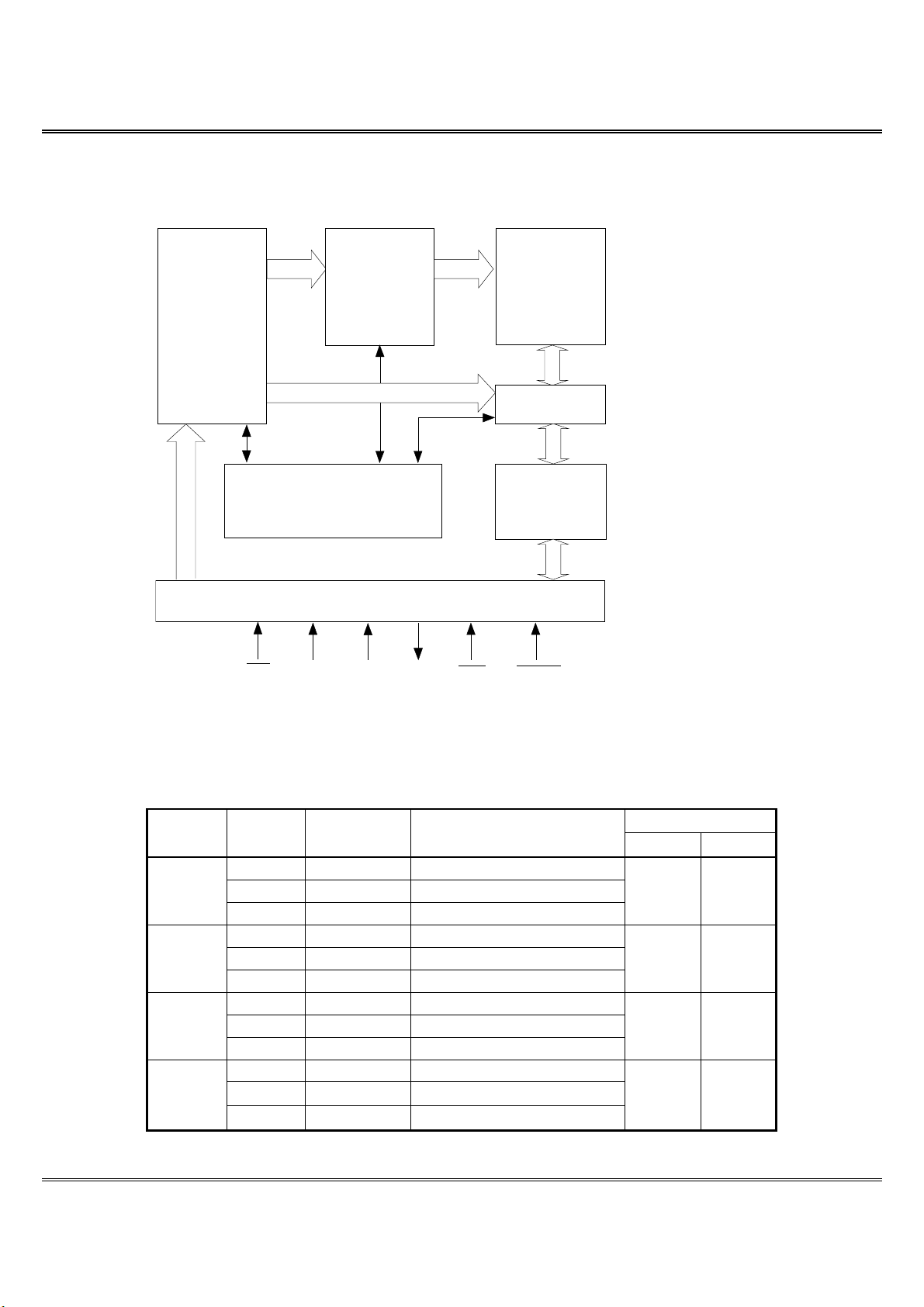
FUNCTIONAL BLOCK DIAGRAM
Address
Buffers
and
Latches
X-Decoder Flash
Y-Decoder
I/O Butters
and
Data Latches
Serial Interface
Control Logic
CE SCK SI WPSO HOLD
SECTOR STRUCTURE
Table 1: F25L02PA Sector Address Table
Block Address
Block Sector Sector Size
(Kbytes) Address range A17 A16
63 4KB 03F000H – 03FFFFH
: : :
3
48 4KB 030000H – 030FFFH
1 1
47 4KB 02F000H – 02FFFFH
: : :
2
32 4KB 020000H – 020FFFH
1 0
31 4KB 01F000H – 01FFFFH
: : :
1
16 4KB 010000H – 010FFFH
0 1
15 4KB 00F000H – 00FFFFH
: : :
0
0 4KB 000000H – 000FFFH
0 0

ESMT
F25L02PA (2F)
Operation Temperature Condition -40
°
C~85
°
C
Elite Semiconductor Memory Technology Inc.
Publication Date: Jan. 2012
Revision:
1.0
5/32
STATUS REGISTER
The software status register provides status on whether the flash
memory array is available for any Read or Write operation,
whether the device is Write enabled, and the state of the memory
Write protection. During an internal Erase or Program operation,
the status register may be read only to determine the completion
of an operation in progress. Table 2 describes the function of
each bit in the software status register.
Table 2: Software Status Register
Bit Name Function Default at
Power-up Read/Write
0 BUSY 1 = Internal Write operation is in progress
0 = No internal Write operation is in progress 0 R
1 WEL 1 = Device is memory Write enabled
0 = Device is not memory Write enabled 0 R
2 BP0 Indicate current level of block write protection (See Table 3) 0 R/W
3 BP1 Indicate current level of block write protection (See Table 3) 0 R/W
4 BP2 Indicate current level of block write protection (See Table 3) 0 R/W
5 TB Top / Bottom write protect 0 R/W
6 RESERVED
Reserved for future use 0 N/A
7 BPL 1 = BP2,BP1,BP0 and TB are read-only bits
0 = BP2,BP1,BP0 and TB are read/writable 0 R/W
Note:
1. Only BP0, BP1, BP2, TB and BPL are writable.
2. BP0, BP1, BP2, TB and BPL are non-volatile.
3. All area are unprotected at power-on (BP2=BP1=BP0=0).
WRITE ENABLE LATCH (WEL)
The Write-Enable-Latch bit indicates the status of the internal
memory Write Enable Latch. If this bit is set to “1”, it indicates the
device is Write enabled. If the bit is set to “0” (reset), it indicates
the device is not Write enabled and does not accept any memory
Write (Program/ Erase) commands. This bit is automatically reset
under the following conditions:
•
Power-up
•
Write Disable (WRDI) instruction completion
•
Page Program instruction completion
•
Sector Erase instruction completion
•
Block Erase instruction completion
•
Chip Erase instruction completion
•
Write Status Register instructions
BUSY
The Busy bit determines whether there is an internal Erase or
Program operation in progress. A “1” for the Busy bit indicates
the device is busy with an operation in progress. A “0” indicates
the device is ready for the next valid operation.
Top/Bottom Block Protect (TB)
The Top/Bottom bit (TB) controls if the Block-Protection (BP2,
BP1, BP0) bits protect from the Top (TB=0) or the Bottom (TB=1)
of the array as show in Table 3, The TB bit can be set with Write
Status Register (WRSR) instruction. The TB bit can not be written
to if the Block- Protection-Look (BPL) bit is 1 or WP is low.

ESMT
F25L02PA (2F)
Operation Temperature Condition -40
°
C~85
°
C
Elite Semiconductor Memory Technology Inc.
Publication Date: Jan. 2012
Revision:
1.0
6/32
Table 3: F25L02PA Block Protection Table
Status Register Bit
Protected Memory Area
Protection Level TB BP2 BP1 BP0 Block Range Address Range
0 X 0 0 0 None None
Upper 1/4 0 0 0 1 Block 3 030000H – 03FFFFH
Upper 1/2 0 0 1 0 Block 2~3 020000H – 03FFFFH
Upper 3/4 0 1 1 0 Block 1~3 010000H – 03FFFFH
Lower 1/4 1 0 0 1 Block 0 000000H – 00FFFFH
Lower 1/2 1 0 1 0 Block 0~1 000000H – 01FFFFH
Lower 3/4 1 1 1 0 Block 0~2 000000H – 02FFFFH
All Blocks X X 1 1 Block 0~3 000000H – 03FFFFH
Block Protection (BP2, BP1, BP0)
The Block-Protection (BP2, BP1, BP0) bits define the size of the
memory area, as defined in Table 3, to be software protected
against any memory Write (Program or Erase) operations. The
Write Status Register (WRSR) instruction is used to program the
BP2, BP1, BP0 bits as long as WP is high or the Block-
Protection-Look (BPL) bit is 0. Chip Erase can only be executed if
Block-Protection bits are all 0. After power-up, BP2, BP1 and BP0
are set to 0.
Block Protection Lock-Down (BPL)
WP pin driven low (V
IL
), enables the Block-Protection-
Lock-Down (BPL) bit. When BPL is set to 1, it prevents any
further alteration of the TB, BPL, BP2, BP1, and BP0 bits. When
the WP pin is driven high (V
IH
), the BPL bit has no effect and its
value is “Don’t Care”. After power-up, the BPL bit is reset to 0.

ESMT
F25L02PA (2F)
Operation Temperature Condition -40
°
C~85
°
C
Elite Semiconductor Memory Technology Inc.
Publication Date: Jan. 2012
Revision:
1.0
7/32
HOLD OPERATION
HOLD pin is used to pause a serial sequence underway with the
SPI flash memory without resetting the clocking sequence. To
activate the HOLD mode, CE must be in active low state. The
HOLD mode begins when the SCK active low state coincides
with the falling edge of the HOLD signal. The HOLD mode ends
when the HOLD signal’s rising edge coincides with the SCK
active low state.
If the falling edge of the HOLD signal does not coincide with the
SCK active low state, then the device enters Hold mode when the
SCK next reaches the active low state.
Similarly, if the rising edge of the HOLD signal does not
coincide with the SCK active low state, then the device exits in
Hold mode when the SCK next reaches the active low state. See
Figure 1 for Hold Condition waveform.
Once the device enters Hold mode, SO will be in high impedance
state while SI and SCK can be V
IL
or V
IH
.
If CE is driven active high during a Hold condition, it resets the
internal logic of the device. As long as HOLD signal is low, the
memory remains in the Hold condition. To resume
communication with the device, HOLD must be driven active
high, and CE must be driven active low. See Figure 22 for Hold
timing.
A c tiv e H o ld A c ti v e H old A c tiv e
H O L D
S C K
Figure 1: HOLD Condition Waveform
WRITE PROTECTION
The device provides software Write Protection.
The Write-Protect pin ( WP ) enables or disables the lock-down
function of the status register. The Block-Protection bits (BP2,
BP1, BP0, TB and BPL) in the status register provide Write
protection to the memory array and the status register. See Table
3 for Block-Protection description.
Write Protect Pin (
WP
)
The Write-Protect ( WP ) pin enables the lock-down function of
the BPL bit (bit 7) in the status register. When WP is driven low,
the execution of the Write Status Register (WRSR) instruction is
determined by the value of the BPL bit (see Table 4). When WP
is high, the lock-down function of the BPL bit is disabled.
Table 4: Conditions to Execute Write-Status-Register (WRSR)
Instruction
WP
BPL
Execute WRSR Instruction
L 1 Not Allowed
L 0 Allowed
H X Allowed

ESMT
F25L02PA (2F)
Operation Temperature Condition -40
°
C~85
°
C
Elite Semiconductor Memory Technology Inc.
Publication Date: Jan. 2012
Revision:
1.0
8/32
INSTRUCTIONS
Instructions are used to Read, Write (Erase and Program), and
configure the F25L02PA. The instruction bus cycles are 8 bits
each for commands (Op Code), data, and addresses. Prior to
executing any Page Program, Write Status Register, Sector
Erase, Block Erase, or Chip Erase instructions, the Write Enable
(WREN) instruction must be executed first. The complete list of
the instructions is provided in Table 5. All instructions are
synchronized off a high to low transition of CE . Inputs will be
accepted on the rising edge of SCK starting with the most
significant bit. CE must be driven low before an instruction is
entered and must be driven high after the last bit of the instruction
has been shifted in (except for Read, Read ID, Read Status
Register, Read Electronic Signature instructions). Any low to high
transition on CE , before receiving the last bit of an instruction
bus cycle, will terminate the instruction in progress and return the
device to the standby mode.
Instruction commands (Op Code), addresses, and data are all
input from the most significant bit (MSB) first.
Table 5: Device Operation Instructions
Bus Cycle
1~3
1 2 3 4 5 6 N
Operation Max.
Freq
S
IN
S
OUT
S
IN
S
OUT
S
IN
S
OUT
S
IN
S
OUT
S
IN
S
OUT
S
IN
S
OUT
S
IN
S
OUT
Read
33 MHz
03H
Hi-Z
A
23
-A
16
Hi-Z
A
15
-A
8
Hi-Z
A
7
-A
0
Hi-Z
X D
OUT0
X D
OUT1
X cont.
Fast Read
13
50 MHz
~
100
MHz
0BH
Hi-Z
A
23
-A
16
Hi-Z
A
15
-A
8
Hi-Z
A
7
-A
0
Hi-Z
X X X D
OUT0
X cont.
Fast Read Dual
Output
11,12
50MHz
~
86 MHz
3BH A
23
-A
16
A
15
-A
8
A
7
-A
0
X D
OUT0~1
cont.
Sector Erase
4
(4K Byte)
20H
Hi-Z
A
23
-A
16
Hi-Z
A
15
-A
8
Hi-Z
A
7
-A
0
Hi-Z
- - - - - -
Block Erase
4,
(64K Byte) D8H
Hi-Z
A
23
-A
16
Hi-Z
A
15
-A
8
Hi-Z
A
7
-A
0
Hi-Z
- - - - - -
Chip Erase
60H /
C7H
Hi-Z
- - - - - - - - - - - -
Page Program
(PP)
02H
Hi-Z
A
23
-A
16
Hi-Z
A
15
-A
8
Hi-Z
A
7
-A
0
Hi-Z
D
IN0
Hi-Z D
IN1
Hi-Z
Up to
256
bytes
Hi-Z
Read Status Register
(RDSR)
6
05H
Hi-Z
X D
OUT
- - - - - - - - - -
Write Status Register
(WRSR)
01H
Hi-Z
D
IN
Hi-Z
- - -. - - - - - - -
Write Enable (WREN)
9
06H
Hi-Z
- - - - - - - - - - - -
Write Disable (WRDI) 04H
Hi-Z
- - - - - - - - - - - -
Deep Power Down (DP) B9h
Hi-Z
- - - - - - - - - - - -
Release from Deep
Power Down (RDP) ABH
Hi-Z
- - - - - - - - - - - -
Read Electronic
Signature (RES)
7
ABH
Hi-Z
X X X
X
X
X
X
11H - - - -
Jedec Read ID
(JEDEC-ID)
8
9FH
Hi-Z
X 8CH
X 30H
X 12H
- - - - - -
00H
Hi-Z
X 8CH
X 11H - -
Read ID (RDID)
10
50 MHz
~
100
MHz
90H
Hi-Z
00H Hi-Z
00H
Hi-Z
01H
Hi-Z
X 11H X 8CH
- -
Note:
1. Operation: S
IN
= Serial In, S
OUT
= Serial Out, Bus Cycle 1 = Op Code
2. X = Dummy Input Cycles (V
IL
or V
IH
); - = Non-Applicable Cycles (Cycles are not necessary); cont. = continuous
3. One bus cycle is eight clock periods.
4. Sector Earse addresses: use A
MS
-A
12
, remaining addresses can be V
IL
or V
IH
Block Earse addresses: use A
MS
-A
16
, remaining addresses can be V
IL
or V
IH
5. To continue programming to the next sequential address location, enter the 8-bit command, followed by the data to be
programmed.
6. The Read-Status-Register is continuous with ongoing clock cycles until terminated by a low to high transition on CE .

ESMT
F25L02PA (2F)
Operation Temperature Condition -40
°
C~85
°
C
Elite Semiconductor Memory Technology Inc.
Publication Date: Jan. 2012
Revision:
1.0
9/32
7. The Read-Electronic-Signature is continuous with on going clock cycles until terminated by a low to high transition on CE .
8. The Jedec-Read-ID is output first byte 8CH as manufacture ID; second byte 30H as memory type; third byte 12H as
memory capacity.
9. The Write-Enable (WREN) instruction and the Write-Status-Register (WRSR) instruction must work in conjunction of each
other. The WRSR instruction must be executed immediately (very next bus cycle) after the WREN instruction to make both
instructions effective. WREN can enable WRSR, user just need to execute it. A successful WRSR can reset WREN.
10. The Manufacture ID and Device ID output will repeat continuously until CE terminates the instruction.
11. Dual commands use bidirectional IO pins. D
OUT
and
cont. are serial data out; others are serial data in.
12. Dual output data:
IO
0
= (D
6
, D
4
, D
2
, D
0
), (D
6
, D
4
, D
2
, D
0
)
IO
1
= (D
7
, D
5
, D
3
, D
1
), (D
7
, D
5
, D
3
, D
1
)
D
OUT0
D
OUT1
13. Max Load capacitance is 15pF.

ESMT
F25L02PA (2F)
Operation Temperature Condition -40
°
C~85
°
C
Elite Semiconductor Memory Technology Inc.
Publication Date: Jan. 2012
Revision:
1.0
10/32
CE
SCK
SI
0 1 2 3 4 5 6 7 8 15 16 23 24 31 32 39 40 47 48 55 56 63 64 80
N+4
D
OUT
N+3
D
OU T
N+2
D
OUT
N+1
D
OUT
N
D
OUT
MSB
MSB
MSB
HIGH IMPENANCE
SO
0B ADD. ADD. ADD.
MODE3
MODE0
71 72
X
Note : X = Dummy Byte : 8 Clocks Input Dummy (V
IL
or V
IH
)
Read (33MHz)
The Read instruction supports up to 33 MHz, it outputs the data
starting from the specified address location. The data output
stream is continuous through all addresses until terminated by a
low to high transition on CE . The internal address pointer will
automatically increment until the highest memory address is
reached. Once the highest memory address is reached, the
address pointer will automatically increment to the beginning
(wrap-around) of the address space, i.e. for 2Mbit density, once
the data from address location 03FFFFH had been read, the next
output will be from address location 000000H.
The Read instruction is initiated by executing an 8-bit command,
03H, followed by address bits [A
23
-A
0
]. CE must remain active
low for the duration of the Read cycle. See Figure 2 for the Read
sequence.
Figure 2: Read Sequence
Fast Read (50 MHz ~ 100 MHz)
The Fast Read instruction supporting up to 100 MHz is initiated
by executing an 8-bit command, 0BH, followed by address bits
[A
23
-A
0
] and a dummy byte. CE must remain active low for the
duration of the Fast Read cycle. See Figure 3 for the Fast Read
sequence.
Following a dummy byte (8 clocks input dummy cycle), the Fast
Read instruction outputs the data starting from the specified
address location. The data output stream is continuous through
all addresses until terminated by a low to high transition on CE .
The internal address pointer will automatically increment until the
highest memory address is reached. Once the highest memory
address is reached, the address pointer will automatically
increment to the beginning (wrap-around) of the address space,
i.e. for 2Mbit density, once the data from address location
03FFFFH has been read, the next output will be from address
location 000000H.
Figure 3: Fast Read Sequence
ESMT
F25L02PA (2F)
Operation Temperature Condition -40
°
C~85
°
C
Elite Semiconductor Memory Technology Inc.
Publication Date: Jan. 2012
Revision:
1.0
11/32
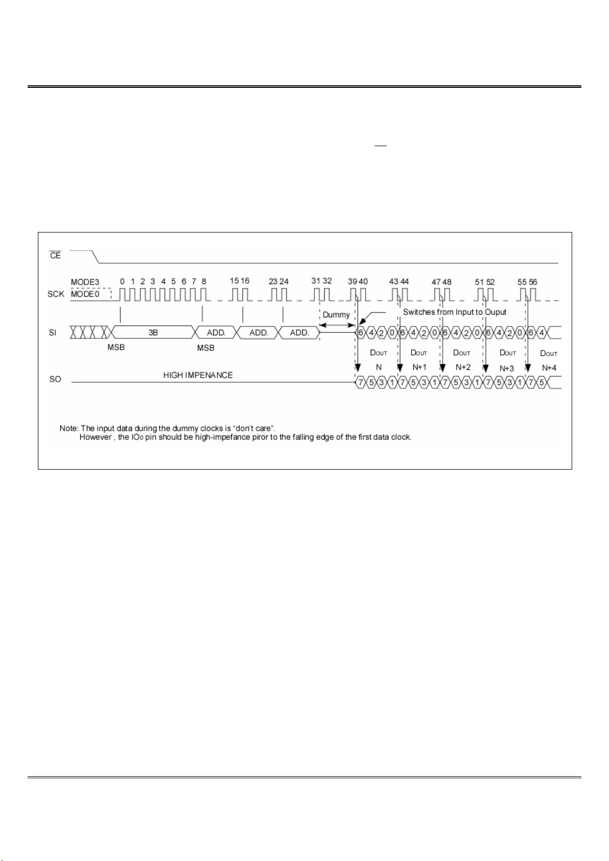
Fast Read Dual Output (50 MHz ~ 86 MHz)
The Fast Read Dual Output (3BH) instruction is similar to the
standard Fast Read (0BH) instruction except the data is output
on SI and SO pins. This allows data to be transferred from the
device at twice the rate of standard SPI devices. This instruction
is for quickly downloading code from Flash to RAM upon
power-up or for applications that cache code- segments to RAM
for execution.
The Fast Read Dual Output instruction is initiated by executing
an 8-bit command, 3BH, followed by address bits [A
23
-A
0
] and a
dummy byte. CE must remain active low for the duration of the
Fast Read Dual Output cycle. See Figure 4 for the Fast Read
Dual Output sequence.
Figure 4: Fast Read Dual Output Sequence

ESMT
F25L02PA (2F)
Operation Temperature Condition -40
°
C~85
°
C
Elite Semiconductor Memory Technology Inc.
Publication Date: Jan. 2012
Revision:
1.0
12/32
Page Program (PP)
The Page Program instruction allows many bytes to be
programmed in the memory. The bytes must be in the erased
state (FFH) when initiating a Program operation. A Page
Program instruction applied to a protected memory area will be
ignored.
Prior to any Write operation, the Write Enable (WREN) instruction
must be executed. CE must remain active low for the duration
of the Page Program instruction. The Page Program instruction is
initiated by executing an 8-bit command, 02H, followed by
address bits [A
23
-A
0
]. Following the address, at least one byte
Data is input (the maximum of input data can be up to 256 bytes).
If the 8 least significant address bits [A
7
-A
0
] are not all zero, all
transmitted data that goes beyond the end of the current page
are programmed from the start address of the same page (from
the address whose 8 least significant bits [A
7
-A
0
] are all zero).
If more than 256 bytes Data are sent to the device, previously
latched data are discarded and the last 256 bytes Data are
guaranteed to be programmed correctly within the same page. If
less than 256 bytes Data are sent to device, they are correctly
programmed at the requested addresses without having any
effects on the other bytes of the same page.
CE must be driven high before the instruction is executed. The
user may poll the Busy bit in the software status register or wait
T
PP
for the completion of the internal self-timed Page Program
operation. While the Page Program cycle is in progress, the Read
Status Register instruction may still be accessed for checking the
status of the Busy bit. It is recommended to wait for a duration of
T
BP
before reading the status register to check the BUSY bit. The
BUSY bit is a 1 during the Page Program cycle and becomes a 0
when the cycle is finished and the device is ready to accept other
instructions again. After the Page Program cycle has finished, the
Write-Enable-Latch (WEL) bit in the Status Register is cleared to
0. See Figure 7 for the Page Program sequence.
Figure 7: Page Program Sequence
ESMT
F25L02PA (2F)
Operation Temperature Condition -40
°
C~85
°
C
Elite Semiconductor Memory Technology Inc.
Publication Date: Jan. 2012
Revision:
1.0
13/32
64K Byte Block Erase
The 64K-byte Block Erase instruction clears all bits in the
selected block to FFH. A Block Erase instruction applied to a
protected memory area will be ignored. Prior to any Write
operation, the Write Enable (WREN) instruction must be
executed. CE must remain active low for the duration of the any
command sequence. The Block Erase instruction is initiated by
executing an 8-bit command, D8H, followed by address bits [A
23
-A
0
]. Address bits [A
MS
-A
16
] (A
MS
= Most Significant address) are
used to determine the block address (BA
X
), remaining address
bits can be V
IL
or V
IH
. CE must be driven high before the
instruction is executed. The user may poll the Busy bit in the
Software Status Register or wait T
BE
for the completion of the
internal self-timed Block Erase cycle. See Figure 8 for the Block
Erase sequence.
Figure 8: 64K-byte Block Erase Sequence
4K Byte Sector Erase
The Sector Erase instruction clears all bits in the selected sector
to FFH. A Sector Erase instruction applied to a protected memory
area will be ignored. Prior to any Write operation, the Write
Enable (WREN) instruction must be executed. CE must remain
active low for the duration of the any command sequence. The
Sector Erase instruction is initiated by executing an 8-bit
command, 20H, followed by address bits [A
23
-A
0
]. Address bits
[A
MS
-A
12
] (A
MS
= Most Significant address) are used to determine
the sector address (SA
X
), remaining address bits can be V
IL
or
V
IH
. CE must be driven high before the instruction is executed.
The user may poll the Busy bit in the Software Status Register or
wait T
SE
for the completion of the internal self-timed Sector Erase
cycle. See Figure 9 for the Sector Erase sequence.
CE
SCK
SI
012345678 15 16 23 24 31
MSB
MSB
HIGH IMPENANCE
S
O
20 ADD. ADD. ADD.
MODE3
MODE0
Figure 9: 4K-byte Sector Erase Sequence

ESMT
F25L02PA (2F)
Operation Temperature Condition -40
°
C~85
°
C
Elite Semiconductor Memory Technology Inc.
Publication Date: Jan. 2012
Revision:
1.0
14/32
Chip Erase
The Chip Erase instruction clears all bits in the device to FFH. A
Chip Erase instruction will be ignored if any of the memory area is
protected. Prior to any Write operation, the Write Enable (WREN)
instruction must be executed. CE must remain active low for
the duration of the Chip-Erase instruction sequence. The Chip
Erase instruction is initiated by executing an 8-bit command, 60H
or C7H. CE must be driven high before the instruction is
executed. The user may poll the Busy bit in the Software Status
Register or wait T
CE
for the completion of the internal self-timed
Chip Erase cycle. See Figure 10 for the Chip Erase sequence.
Figure 10: Chip Erase Sequence
Read Status Register (RDSR)
The Read Status Register (RDSR) instruction allows reading of
the status register. The status register may be read at any time
even during a Write (Program/Erase) operation.
When a Write operation is in progress, the Busy bit may be
checked before sending any new commands to assure that the
new commands are properly received by the device.
CE must be driven low before the RDSR instruction is entered
and remain low until the status data is read. Read Status
Register is continuous with ongoing clock cycles until it is
terminated by a low to high transition of the CE . See Figure 11
for the RDSR instruction sequence.
Figure 11: Read Status Register (RDSR) Sequence
CE
SCK
SI
0 1 2 3 4 5 6 7
MSB
HIGH IMPENANCE
S
O
60 or C7
MODE3
MODE0

ESMT
F25L02PA (2F)
Operation Temperature Condition -40
°
C~85
°
C
Elite Semiconductor Memory Technology Inc.
Publication Date: Jan. 2012
Revision:
1.0
15/32
Write Enable (WREN)
The Write Enable (WREN) instruction sets the Write-Enable-
Latch bit in the Software Status Register to 1 allowing Write
operations to occur.
The WREN instruction must be executed prior to any Write
(Program/Erase) operation. CE must be driven high before the
WREN instruction is executed.
Figure 12: Write Enable (WREN) Sequence
Write Disable (WRDI)
The Write Disable (WRDI) instruction resets the Write-Enable-
Latch bit to 0 disabling any new Write operations from occurring. CE must be driven high before the WRDI instruction is
executed.
Figure 13: Write Disable (WRDI) Sequence
CE
SCK
SI
0 1 2 3 4 5 6 7
MSB
HIGH IMPENANCE
S
O
06
MODE3
MODE0
CE
SCK
SI
0 1 2 3 4 5 6 7
MSB
HIGH IMPENANCE
S
O
04
MODE3
MODE0

ESMT
F25L02PA (2F)
Operation Temperature Condition -40
°
C~85
°
C
Elite Semiconductor Memory Technology Inc.
Publication Date: Jan. 2012
Revision:
1.0
16/32
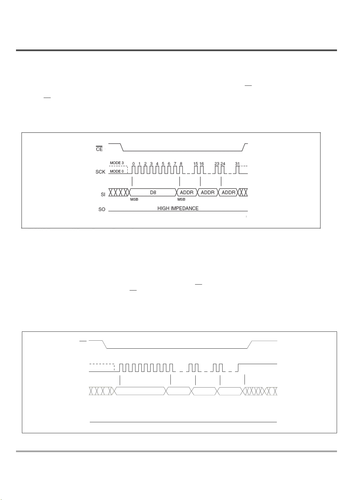
Write-Status-Register (WRSR)
The Write Status Register instruction writes new values to the
BP2, BP1, BP0, TB and BPL bits of the status register. CE
must be driven low before the command sequence of the WRSR
instruction is entered and driven high before the WRSR
instruction is executed. See Figure 14 for WREN and WRSR
instruction sequences.
Executing the Write Status Register instruction will be ignored
when WP is low and BPL bit is set to “1”. When the WP is
low, the BPL bit can only be set from “0” to “1” to lock down the
status register, but cannot be reset from “1” to “0”.
When WP is high, the lock-down function of the BPL bit is
disabled and the BPL, TB, BP0, BP1,and BP2 bits in the status
register can all be changed. As long as BPL bit is set to 0 or WP
pin is driven high (V
IH
) prior to the low-to-high transition of the
CE pin at the end of the WRSR instruction, the bits in the status
register can all be altered by the WRSR instruction. In this case,
a single WRSR instruction can set the BPL bit to “1” to lock down
the status register as well as altering the TB, BP0; BP1 and BP2
bits at the same time. See Table 4 for a summary description of
WP and BPL functions.
Figure 14: Write-Enable (WREN) and Write-Status-Register (WRSR)
CE
SCK
SI
0 1 2 3 4 5 6 7
MSBMSB
HIGH IMPENANCE
S
O
06
MODE3
MODE0
7 6 54 3 2 10
01
0 1 2 3 4 5 6 7 8 9 10 11 12 13 14 15
Stauts Register
Data In

ESMT
F25L02PA (2F)
Operation Temperature Condition -40
°
C~85
°
C
Elite Semiconductor Memory Technology Inc.
Publication Date: Jan. 2012
Revision:
1.0
17/32
Deep Power Down (DP)
The Deep Power Down instruction is for minimizing power
consumption (the standby current is reduced from I
SB1
to I
SB2
.).
This instruction is initiated by executing an 8-bit command, B9H,
and then CE must be driven high. After CE is driven high, the
device will enter to deep power down within the duration of T
DP
.
Once the device is in deep power down status, all instructions will
be ignored except the Release from Deep Power Down
instruction (RDP) and Read Electronic Signature instruction
(RES). The device always power-up in the normal operation with
the standby current (I
SB1
). See Figure 15 for the Deep Power
Down instruction.
Figure 15: Deep Power Down Instruction
Release from Deep Power Down (RDP) and Read-Electronic-Signature (RES)
The Release form Deep Power Down and Read-Electronic-
Signature instruction is a multi-purpose instruction.
The instruction can be used to release the device from the deep
power down status. This instruction is initiated by driving CE
low and executing an 8-bit command, ABH, and then drive CE
high. See Figure 16 for RDP instruction. Release from the deep
power down will take the duration of T
RES1
before the device will
resume normal operation and other instructions are accepted.
CE must remain high during T
RES1
.
The instruction also can be used to read the 8-bit Electronic-
Signature of the device on the SO pin. It is initiated by driving
CE low and executing an 8-bit command, ABH, followed by 3
dummy bytes. The Electronic-Signature byte is then output from
the device. The Electronic-Signature can be read continuously
until CE go high. See Figure 17 for RES sequence. After
driving CE high, it must remain high during for the duration of
T
RES2
, and then the device will resume normal operation and
other instructions are accepted.
The instruction is executed while an Erase, Program or WRSR
cycle is in progress is ignored and has no effect on the cycle in
progress.
SCK
0 1 2 3 4 5 6 7MODE3
MODE0
SI
CE
Standard Current
T
DP
MSB
B9
Deep Power Down Current
(I
SB2
)
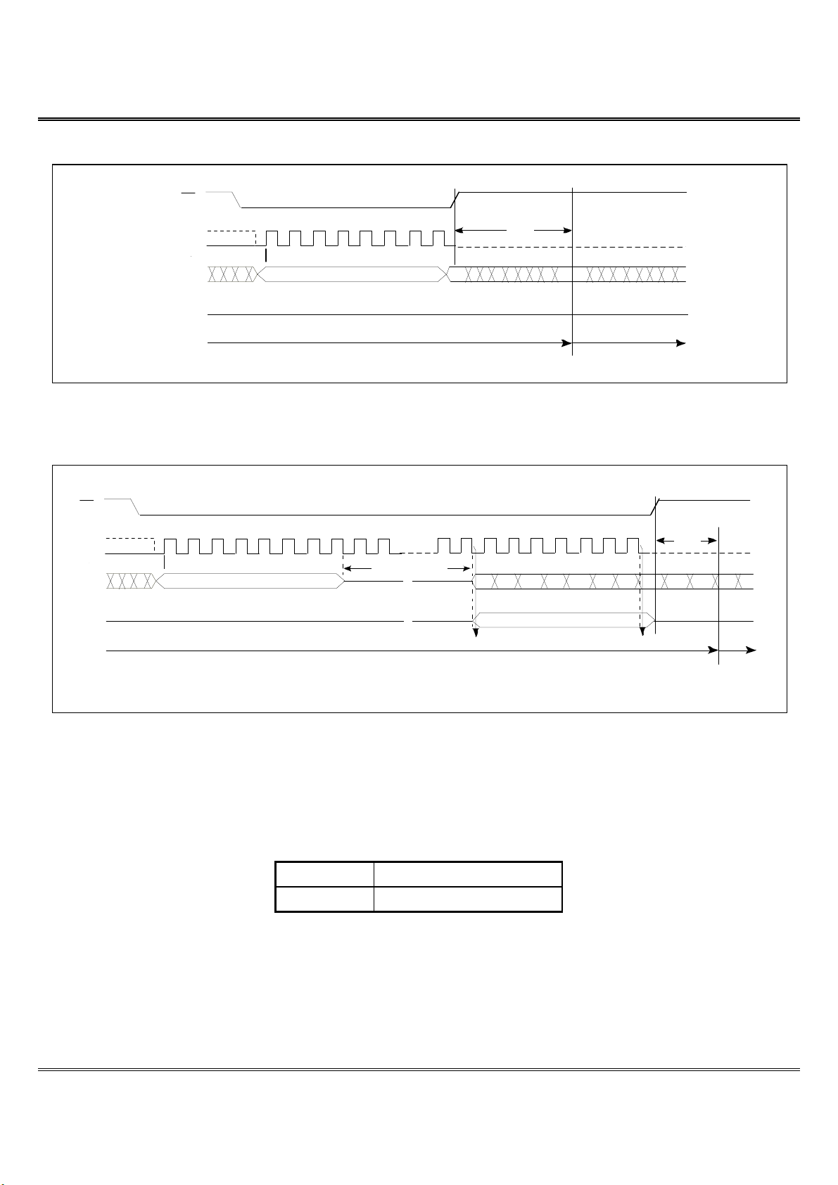
ESMT
F25L02PA (2F)
Operation Temperature Condition -40
°
C~85
°
C
Elite Semiconductor Memory Technology Inc.
Publication Date: Jan. 2012
Revision:
1.0
18/32
Figure 16: Release from Deep Power Down (RDP) Instruction
Figure 17: Read Electronic -Signature (RES) Sequence
Table 6: Electronic Signature Data
Command Electronic Signature Data
RES 11H
SCK
0 1 2 3 4 5 6 7MODE3
MODE0
SI
CE
Standby Current
T
RES1
MSB
AB
Deep Power Down Current
(
I
SB2
)
SO
HIGH IMPEDANCE
SCK
0 1 2 3 4 5 6 7 8 9
MODE3
MODE0
SI
CE
Standby
Current
T
RES2
MSB
AB
Deep Power Down Current
(
I
SB2
)
SO
HIGH IMPEDANCE
SS
30 31 32 33 34 35 36 37 38
SS
Electronic-Signature Data Out
SS
MSB
3 Dummy Bytes

ESMT
F25L02PA (2F)
Operation Temperature Condition -40
°
C~85
°
C
Elite Semiconductor Memory Technology Inc.
Publication Date: Jan. 2012
Revision:
1.0
19/32
JEDEC Read-ID
The JEDEC Read-ID instruction identifies the device as
F25L02PA and the manufacturer as ESMT. The device
information can be read from executing the 8-bit command, 9FH.
Following the JEDEC Read-ID instruction, the 8-bit
manufacturer’s ID, 8CH, is output from the device. After that, a
16-bit device ID is shifted out on the SO pin. Byte1, 8CH,
identifies the manufacturer as ESMT. Byte2, 30H, identifies the
memory type as SPI Flash. Byte3, 12H, identifies the device as
F25L02PA. The instruction sequence is shown in Figure 18.
The JEDEC Read ID instruction is terminated by a low to high
transition on CE at any time during data output. If no other
command is issued after executing the JEDEC Read-ID
instruction, issue a 00H (NOP) command before going into
Standby Mode ( CE =V
IH
).
Figure 18: JEDEC Read-ID Sequence
Table 7: JEDEC READ-ID Data
Device ID
Manufacturer’s ID
(Byte 1) Memory Type
(Byte 2)
Memory Capacity
(Byte 3)
8CH 30H 12H
CE
SCK
SI
MSB
HIGH IMPENANCE
SO
9F
MODE3
MODE0
0 1 2 3 4 5 6 7 8 9 10 11 12 13 1415 1617 1819 2021 22 23 24 25 2627 2829 3031
8C
M
S
B
30 12
M
S
B
MSB

ESMT
F25L02PA (2F)
Operation Temperature Condition -40
°
C~85
°
C
Elite Semiconductor Memory Technology Inc.
Publication Date: Jan. 2012
Revision:
1.0
20/32
Read-ID (RDID)
The Read-ID instruction (RDID) identifies the devices as
F25L02PA and manufacturer as ESMT. This command is
backward compatible to all ESMT SPI devices and should be
used as default device identification when multiple versions of
ESMT SPI devices are used in one design. The device
information can be read from executing an 8-bit command, 90H,
followed by address bits [A
23
-A
0
]. Following the Read-ID
instruction, the manufacturer’s ID is located in address 000000H
and the device ID is located in address 000001H.
Once the device is in Read-ID mode, the manufacturer’s and
device ID output data toggles between address 000000H and
000001H until terminated by a low to high transition on CE .
Figure 19: Read-ID Sequence
Table 8: Product ID Data
Address Byte1 Byte2
8CH 11H
000000H
Manufacturer’s ID Device ID
ESMT F25L02PA
11H 8CH
000001H Device ID
ESMT F25L02PA Manufacturer’s ID
CE
SCK
SI
0 1 2 3 4 5 6 7 8 15 16 23 24 31 32 39 40 47 48 55 56 63
MSB
MSB
HIGH IMPENANCE
SO
90 0 0 00 ADD
1
MODE3
MODE0
Note: The Manufacture’s an d Device ID output stream is continuous until terminated by a low to high transition on CE.
1
.
0
0
H
w
i
l
l
o
u
t
p
u
t
t
h
e
M
a
n
u
f
a
c
t
u
r
e
’
s
I
D
f
i
r
s
t
a
n
d
0
1
H
w
i
l
l
o
u
t
p
u
t
D
e
v
i
c
e
I
D
f
i
r
s
t
b
e
f
o
r
e
t
o
g
g
l
i
n
g
b
e
t
w
e
e
n
t
h
e
t
w
o
.
.
HIGH
IMPENANCE
8C 8C11 11
MSB
This manual suits for next models
9
Table of contents
Other ESMT Storage manuals


