Forlinx FET6254-C User manual


Hardware manual
OK3568-C FET3568-C
www.forlinx.net
- 2 -
Update record
Date
Manual
version
SoM
version
Carrier board
version
Update record
July, 2022
V1.0
V1.1
V1.1
First edition

Hardware manual
OK6254-C FET6254-C
www.forlinx.net
- 3 -
Content
Update record ............................................................................................................................................- 2 -
Content ......................................................................................................................................................- 3 -
Chapter 1 Overview of AM62x ................................................................................................................ - 8 -
Chapter 2 Introduction of FET6254-C SoM .............................................................................................- 9 -
2.1 FET6254-C Exterior .................................................................................................................... - 9 -
2.2 FET6254-C Mechanical Dimensions(Top layer+ bottom layer) ................................................. - 9 -
2.3 FET6254-C Features ..................................................................................................................- 10 -
2.3.1 Frequency .........................................................................................................................- 10 -
2.3.2 Power Supply ...................................................................................................................- 10 -
2.3.3 Working Environment ......................................................................................................- 10 -
2.3.4 SoM Interface Speed ........................................................................................................- 11 -
2.4 SoM Resource ............................................................................................................................ - 11 -
2.5 SoM FET6254-C Pin Definition ................................................................................................- 13 -
2.5.1 Schematic .........................................................................................................................- 13 -
2.5.2 SoM FET6254-C Pins Spec. ............................................................................................- 16 -
2.6 SoM Pin Spec. ............................................................................................................................- 25 -
2.6.1 Power Pin .........................................................................................................................- 25 -
2.6.2 Boot Pin ........................................................................................................................... - 27 -
2.6.3 LVDS Output Pin ............................................................................................................. - 28 -
2.6.4 MIPI CSI ..........................................................................................................................- 28 -
2.6.5 USB ..................................................................................................................................- 29 -
2.6.6 Ethernet ............................................................................................................................- 29 -
2.6.7 CPTS ................................................................................................................................- 30 -
2.6.8 DSS(Display Subsystem) .................................................................................................- 30 -
2.6.9 ECAP ............................................................................................................................... - 31 -
2.6.10 Emulation and Debug .................................................................................................... - 31 -
2.6.11 EPWM ............................................................................................................................- 32 -
2.6.12 EQEP ............................................................................................................................. - 33 -
2.6.13 GPMC ............................................................................................................................ - 33 -
2.6.14 IIC .................................................................................................................................. - 36 -
2.6.15 MCAN ........................................................................................................................... - 37 -
2.7.16 MCASP ..........................................................................................................................- 37 -
2.7.17 MCSPI ........................................................................................................................... - 39 -
2.7.18 MDIO .............................................................................................................................- 40 -
2.7.19 MMC ..............................................................................................................................- 40 -
2.7.20 OSPI ...............................................................................................................................- 41 -
2.7.21 System Pins ....................................................................................................................- 41 -

Hardware manual
OK6254-C FET6254-C
www.forlinx.net
- 4 -
2.7.22 TIMER ........................................................................................................................... - 42 -
2.7.23 UART.............................................................................................................................- 43 -
2.7 SoM Designing Tips .................................................................................................................. - 46 -
Chapter 3 OK6254-C Carrier Board Features ........................................................................................ - 47 -
3.1 Overview ....................................................................................................................................- 47 -
3.2 Dimensions ................................................................................................................................ - 48 -
3.3 Carrier Board Features ...............................................................................................................- 48 -
3.4 Carrier Board Introduction .........................................................................................................- 49 -
3.5.1 Power ............................................................................................................................... - 49 -
3.5.2 Reset .................................................................................................................................- 51 -
3.5.3 Boot Mode ....................................................................................................................... - 51 -
3.5.4 Debug Port ....................................................................................................................... - 53 -
3.5.5 JTAG ................................................................................................................................ - 53 -
3.5.6 LED and User Key ...........................................................................................................- 54 -
3.5.7 Display ............................................................................................................................. - 55 -
3.5.8 Video Input .......................................................................................................................- 57 -
3.5.9 TF Card ............................................................................................................................ - 57 -
3.5.10 Ethernet ..........................................................................................................................- 58 -
3.5.11 USB ................................................................................................................................- 59 -
3.5.12 4G/ 5G ............................................................................................................................- 60 -
3.5.13 WiFi& BT ...................................................................................................................... - 61 -
3.5.14 Audio ..............................................................................................................................- 62 -
3.5.15 RTC ................................................................................................................................- 63 -
3.5.16 QSPI Flash ..................................................................................................................... - 63 -
3.5.17 GPMC ............................................................................................................................ - 64 -
3.5.18 PCIe2.1 .......................................................................................................................... - 64 -
3.5.18 CAN&RS485 ................................................................................................................. - 65 -
3.5.19 EEPROM ....................................................................................................................... - 66 -
3.5.20 MCU Pins for Users .......................................................................................................- 66 -
Appendix .................................................................................................................................................- 67 -
Appendix 1 Carrier Board Designing Instruction ............................................................................- 67 -
Appendix 2 Power Consumption .....................................................................................................- 68 -
Appendix 3 Connector Dimensions .................................................................................................- 68 -
Appendix 4 Minimum System Schematic ....................................................................................... - 71 -

Hardware manual
OK6254-C FET6254-C
www.forlinx.net
- 5 -
Attentions
MUST READ BEFORE WORKING WITH THE BOARD
Product Operation Environment:
Hot-plug of system on module and peripheral modules is strictly prohibited.
Please follow all the warnings and instructions marked on the product.
Please keep the product dry. Once splashed or immersed by any liquid, cut off the power and
dry it out immediately.
Please store and operate the product in ventilating conditions to avoid damages brought by
over high temperature.
Please do not use or store the product in dusty or untidy conditions.
Please do not use or store the product in alternate cold and hot conditions to avoid
condensing which will damage components.
Please do not treat the product rudely. Any falling-off, knocking and violate shaking may cause
destruction to circuit and components.
Please do not clean the product with organic solvents or corrodible liquids.
Please do not dismantle or repair the product by yourself. Contact us when the product
malfunctions.
Please do not modify the product by yourself or use fittings unauthorized by us. Otherwise,
the damage caused by that will be on your part and not included in guarantee terms.
Any questions please feel free to contact the sales engineer or Forlinx Technical Service department.

Hardware manual
OK6254-C FET6254-C
www.forlinx.net
- 6 -
Copyright Announcement
Please note that reproduction of this User Manual in whole or in part, without express written permission from Forlinx, is
not permitted.

Hardware manual
OK6254-C FET6254-C
www.forlinx.net
- 7 -
Technical Support and Customization
1. Technical Support Range
1.1 Forlinx product related hardware and software source consulting;
1.2 Problems related to our software and hardware manual;
1.3 After-sale technical support for ODM product;
1.4 Forlinx product related trouble shooting, failure diagnose and related maintenance
2. Range of Technical Discussion ( non-compulsory)
2.1 Modification and comprehension of source code;
2.2 How to implant OS;
2.3 Software and hardware problems occured in self-modifying and programming
Note: the above three points are out of Forlinx technical service range, but Forlinx will try best but can
not promise to help users to solve the problems.
3. Accesses to Technical Support
3.1 If you are able to understand Chinese, you can try to all the technical persons directly, the tel. number
(non-instant messenger) is 0086-312-3119192
3.2 Any Forlinx product related questions or help if you need, you can send email to corresponding sales
engineer whom you keep in touch with, the sales engineer will help you to follow up your issue and get
back to you soonest;
3.3 If you are not able to call the technical person and don’t whom you should send email to, then you can
4. Access to Materials
Forlinx product related technical files will be uploaded to dropbox, when you get the board, please take
your Dropbox account to create a folder and share it with Forlinx([email protected]), Forlinx will pass
the related technical files to the shared folder.

Hardware manual
OK6254-C FET6254-C
www.forlinx.net
- 8 -
Chapter 1 Overview of AM62x
The low-cost AM62x Sitara™ MPU family of application processors are built for Linux® application
development. With scalable 64-bit Arm® Cortex®-A53 performance and embedded features, such as:
dual-display support and 3D graphics acceleration, along with an extensive set of peripherals that make
the AM62x device well-suited for a broad range of industrial and automotive applications while offering
intelligent features and optimized power architecture as well.
The 2-port Gigabit Ethernet switch has one internal port and two external ports with Time-Sensitive
Networking (TSN) support. An additional PRU module on the device enables real-time I/O capability for
customer’s own use cases. In addition, the extensive set of peripherals included in AM62x enables
system-level connectivity, such as: USB, MMC/SD, Camera interface, OSPI, CAN-FD and GPMC for
parallel host interface to an external ASIC/FPGA. The AM62x device also supports secure boot for IP
protection with the built-in Hardware Security Module (HSM) and employs advanced power management
support for portable and power-sensitive applications
Some of these applications include:
• Industrial HMI
• EV charging stations
• Touchless building access
• Driver monitoring systems(DMS/ OMS)/ ICM
• Retail automation
• TCU
• 3D Point Cloud
• V2X/ V2V
Hardware manual
OK6254-C FET6254-C
www.forlinx.net
- 9 -
Chapter 2 Introduction of FET6254-C SoM
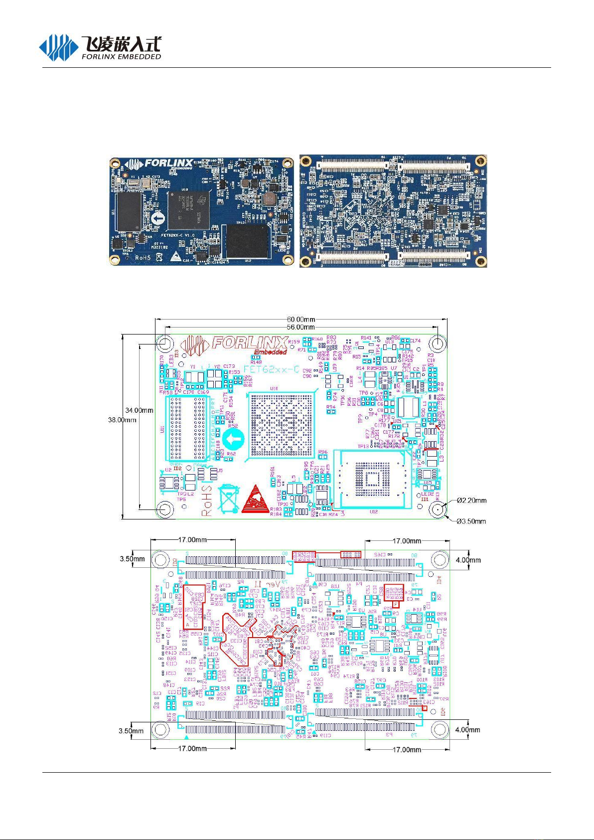
2.1 FET6254-C Exterior
2.2 FET6254-C Mechanical Dimensions(Top layer+ bottom layer)
3
Hardware manual
OK6254-C FET6254-C
www.forlinx.net
- 10 -
Dimensions: 60x 38mm, tolerance ±0.15mm
Processing: 1.6mm thickness, 10-layer ENIG PCB
Package: four 80-pin connectors with pitch of 0.5mm, SoM connector model is AXK6F80337YG, and
mating carrier board connector model is AXK5F80537YG, about connector diagram please refer to the
appendix.
The SoM is preserved with four holes with diameter of 2.2mm on its four corners which could be used for
reinforcement purpose in case of vibration circumstances.
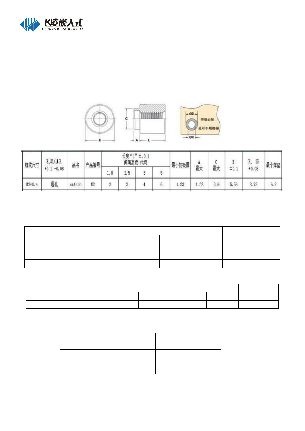
Users can take Forlinx designing for reference, use M2, L=2mm mounting nuts as below
2.3 FET6254-C Features
2.3.1 Frequency
Item
Spec.
Note
Minimum
Typical
Maximum
Unit
Arm® Cortex®-53
--
--
1400
MHz
--
Arm® Cortex®-M4F
--
--
400
MHz
RTC
--
32.768
--
KHz
--
2.3.2 Power Supply
Item
Pin mark
Spec.
Note
Minimum
Typical
Maximum
Unit
Main power
ACIN
4.5
5.0
5.5
V
--
2.3.3 Working Environment
Item
Spec.
Note
Mini
Classic
Max
Unit
Temp width
Working
-40
25
+85
℃
Industrial grade
Storage
-40
25
+85
℃
RH
Working
10
--
90
% RH
Non-condensing
Storage
5
--
95
% RH
Hardware manual
OK6254-C FET6254-C
www.forlinx.net
- 11 -
2.3.4 SoM Interface Speed
Item
Spec.
Note
Minimum
Typical
Maximum
Unit
UART
—
115200
3.6M
bps
--
SPI
—
—
50
MHz
IIC
—
100
400
Kbps
CAN FD
—
—
5
Mbps
USB
—
--
480
Mbps
--
2.4 SoM Resource
Peripheral
QTY
Spec.
LVDS*1*2
2
Two 4-lane LVDS with each lane up to 1.19Gbps;
A single LVDS is up to(1920 x 1200@60fps, 162MHz)
Can support below modes
Single LVDS output;
2x single LVDS(same content);
Dual LVDS output: 8-lane data and 2-lane clock combine to one display output
RGB Parallel
1
1x 24-bit RGB parallel interface, up to WUXGA(1920x 1200@60FPS, 165MHz)
MIPI CSI
1
1x 4-lane MIPI CSI
MIPI-DPHY 1.2
Support 1/ 2/ 3/ 4-wire mode, each up to 2.5Gbps
Ethernet
2
RMII(10/100) or RGMII(10/ 100/ 1000)
Supports IEEE1588(Annex D,Annex E, Annex F with 802.1AS PTP)
Supports TSN
Supports hardware IP/ UDP/ TCP verify and unload
USB
2
USB2.0 up to 480Mbps
Can be configured to USB host, USB device or USB dual-role device(DRD)
Integrated with USB VBUS
UART*3
≤9
Compatible with 16C750
Supports RS485 external transceiver auto current control
Rating up to 3.6Mbps baud rate
Supports stop-bit: 1, 1.5, 2 bit(s)
Parity: odd, even, none
SPI*4
≤5
Each lane has programmable frequency, polarity and phase serial clock
MCSPI is up to 50MHz
I2C*5
≤6
Supports standard mode(up to 100Kbps) and high speed mode(up to 400Kbps)
7-bit and 10-bit device addressing
Audio
≤3
Sending and receiving clock up to 50MHz
Supports TDM, Iner-IC Sound(I2X) and similar forms
Supports digital audio(SPDIF, IEC60958-1 and AES-3)
Supports audio reference output clock

Hardware manual
OK6254-C FET6254-C
www.forlinx.net
- 12 -
ePWM
≤3
Each pair PWM supports two PWM output(EPWMxA and EPWMxB) applicable for
below configuration
1. Two separate PWM output, single edge operating;
2. Two independent PWM outputs with bilateral symmetrical operation;
3. One independent PWM output with bilateral asymmetric operation,
4. Generated dead-band with independent rising and falling edge delay control
eQEP
≤3
Enhanced quadrature encoder pulse input
Supports input synchronization;
Supports quadrature encoder unit;
Supports position counters and control units for position measurement;
Supports quadrature edge capture unit for low-speed measurements
eCAP
≤3
Audio input sampling rate measurement;
Speed measurement of rotating machinery (e.g. toothed sprockets sensed by Hall sensors);
Elapsed time measurement between position sensor pulses;
Period and duty cycle measurements of pulse train signals;
Decode current or voltage magnitude from duty cycle encoded current/voltage sensors
CAN-FD*6
≤3
Complies with CAN2.0A, CAN2.0B or ISO 11898-1 protocols;
Supports complete CAN FD(up to 64 bytes)
Supports RAM parity/ ECC;
Rating up to 5Mbps
SD
≤2
2x 4-bit SD/ SDIO, up to UHS-I;
Complies with eMMC5.1, SD3.0 and SDIO3.0
GPMC
1
Up to 133MHz
Flexible 8-bit and 16-bit asynchronous memory interface, can be mounted with up to 4
chipsets(22-bit address)
Applicable for NAND, Nor, Muxed-Nor and SRAN
OSPI/ QSPI
1
166MHz DDR/200MHz SDR
JTAG
1
supported
Note:
1. Single LVDS can support WUXGA(1920x 1200@ 60p, 162MHz), it needs the receiving monitor or lin
A bridge device can accept the device's video output over a single LVDS link. Generally, it’s only used
when display resolution less than 1366x 768. in dual-link mode, the second interface won’t enlarge the
band width, but reduce the required pixel cock to half.
2. Supports 1 x 2048x1080 + 1 x 1280x720;
3. 7 among the 9 UART are resource of the main domain, and the other 2 are resource of MCU domain,
MCU domain names are WKUP_UART0, MCU_UART0;
4. 3 among the 5 SPI are resource of the main domain, and the other 2 are resource of MCU domain;
5. 4 among the 6 IIC are resource of the main domain, and the other 2 are resource of MCU domain;
6. 1 among 3 CAN is resouce of the main domain, and the other 2 are resource of the MCU domain

Hardware manual
OK6254-C FET6254-C
www.forlinx.net
- 13 -
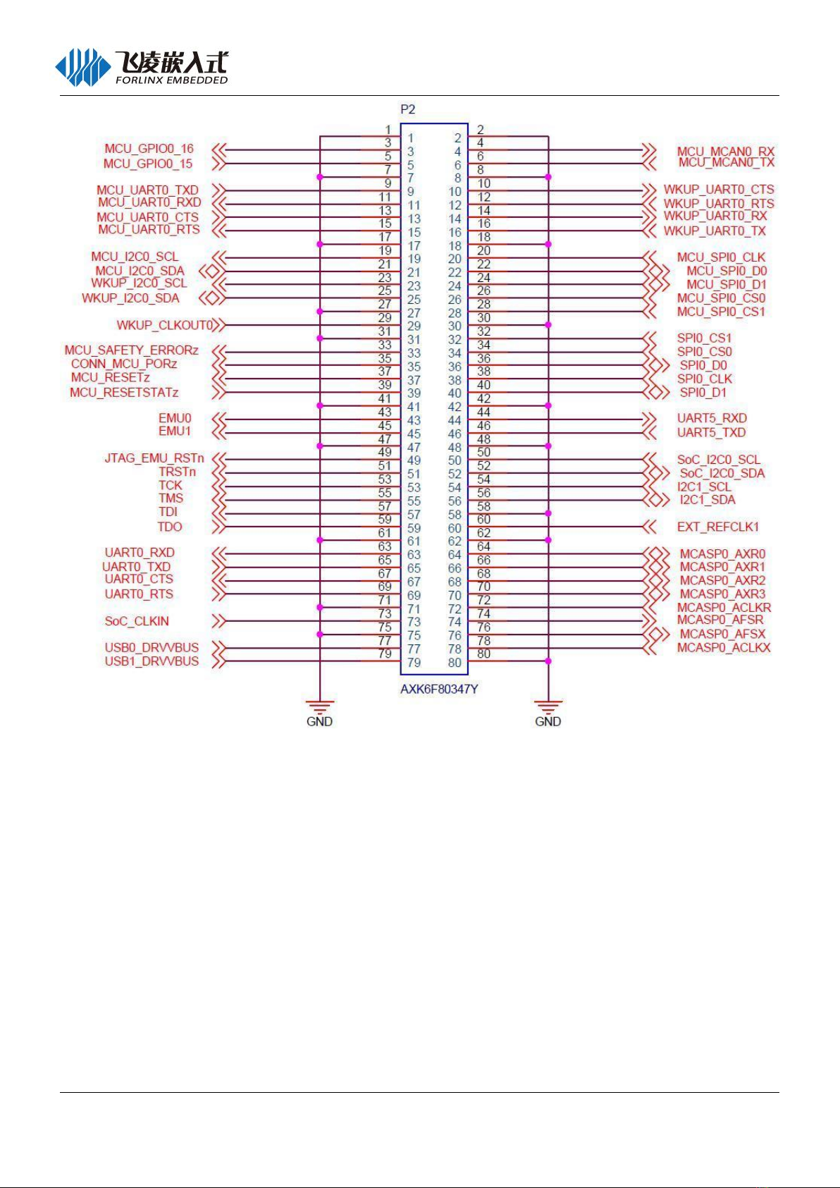
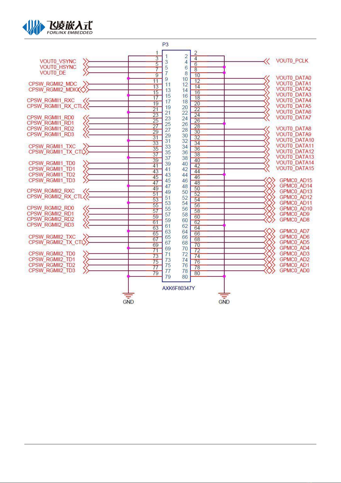
2.5 SoM FET6254-C Pin Definition
2.5.1 Schematic
Hardware manual
OK6254-C FET6254-C
www.forlinx.net
- 14 -
Hardware manual
OK6254-C FET6254-C
www.forlinx.net
- 15 -

Hardware manual
OK6254-C FET6254-C
www.forlinx.net
- 16 -
2.5.2 SoM FET6254-C Pins Spec.
Note
Subscript
Spec.
[1]
PIN can be configured to interrupt
[2]
The default power is 1.8V
[3]
PINs are related to CPU boot, not
recommended to be used as IO.
[4]
Dedicated PIN, cannot be used as IO
Hardware manual
OK6254-C FET6254-C
www.forlinx.net
- 17 -
Table 1 LEFT_UP (P1 ) connector pins (odd)
NUM
BALL
Signal name
GPIO
VOL
Pin description
Default function
1
-
GND
-
-
Ground
GND
3
-
CH1_LVDS_A0P
-
-
CH1_LVDS data A0+
CH1_LVDS_A0P
5
-
CH1_LVDS_A0N
-
-
CH1_LVDS data A0-
CH1_LVDS_A0N
7
-
GND
-
-
Ground
GND
9
-
CH1_LVDS_A1P
-
-
CH1_LVDS data A1+
CH1_LVDS_A1P
11
-
CH1_LVDS_A1N
-
-
CH1_LVDS data A1-
CH1_LVDS_A1N
13
-
GND
-
-
Ground
GND
15
-
CH1_LVDS_A2P
-
-
CH1_LVDS data A2+
CH1_LVDS_A2P
17
-
CH1_LVDS_A2N
-
-
CH1_LVDS data A2-
CH1_LVDS_A2N
19
-
GND
-
-
Ground
GND
21
-
CH1_LVDS_CLKP
-
-
CH1_LVDS clock +
CH1_LVDS_CLKP
23
-
CH1_LVDS_CLKN
-
-
CH1_LVDS clock- _
CH1_LVDS_CLKN
25
-
GND
-
-
Ground
GND
27
-
CH1_LVDS_A3P
-
-
CH1_LVDS data A3+
CH1_LVDS_A3P
29
-
CH1_LVDS_A3N
-
-
CH1_LVDS data A3-
CH1_LVDS_A3N
31
-
GND
-
-
Ground
GND
33
-
CH2_LVDS_CLKN
-
-
CH2_LVDS clock- _
CH2_LVDS_CLKN
35
-
CH2_LVDS_CLKP
-
-
CH2_LVDS clock +
CH2_LVDS_CLKP
37
-
GND
-
-
Ground
GND
39
-
CH2_LVDS_A1N
-
-
CH2_LVDS data A1-
CH2_LVDS_A1N
41
-
CH2_LVDS_A1P
-
-
CH2_LVDS data A1+
CH2_LVDS_A1P
43
-
GND
-
-
Ground
GND
45
-
CH2_LVDS_A2N
-
-
CH2_LVDS data A2-
CH2_LVDS_A2N
47
-
CH2_LVDS_A2P
-
-
CH2_LVDS data A2+
CH2_LVDS_A2P
49
-
GND
-
-
Ground
GND
51
-
CH2_LVDS_A0P
-
-
CH2_LVDS data A0+
CH2_LVDS_A0P
53
-
CH2_LVDS_A0N
-
-
CH2_LCDS data A0-
CH2_LVDS_A0N
55
-
GND
-
-
Ground
GND
57
-
CH2_LVDS_A3P
-
-
CH2_LVDS data A3+
CH2_LVDS_A3P
59
-
CH2_LVDS_A3N
-
-
CH2_LVDS data A3-
CH2_LVDS_A3N
61
-
GND
-
-
Ground
GND
63
-
GND
-
-
Ground
GND
65
-
USB1_DP
-
-
USB1 Data +
USB1_DP
67
-
USB1_DM
-
-
USB1 data- _
USB1_DM
69
-
GND
-
-
Ground
GND
71
-
GND
-
-
Ground
GND
73
-
USB0_DP
-
-
USB0 data +
USB0_DP
75
-
USB0_DM
-
-
USB0 data- _
USB0_DM
77
-
GND
-
-
Ground
GND
Hardware manual
OK6254-C FET6254-C
www.forlinx.net
- 18 -
79
-
GND
-
-
Ground
GND
Table 2 LEFT_UP (P1 ) connector pins (even)
Num
Ball
Signal
GPIO
Vol
Spec.
Default function
2
-
GND
-
-
Ground
GND
4
-
CSI0_RXCLKP
-
-
MIPI_CSI0 receive clock +
CSI0_RXCLKP
6
-
CSI0_RXCLKN
-
-
MIPI_CSI0 receive clock -
CSI0_RXCLKN
8
-
GND
-
-
Ground
GND
10
-
CSI0_RXP3
-
-
MIPI_CSI0 receive data 3+
CSI0_RXP3
12
-
CSI0_RXN3
-
-
MIPI_CSI0 receive data 3-
CSI0_RXN3
14
-
GND
-
-
Ground
GND
16
-
CSI0_RXP1
-
-
MIPI_CSI0 receive data 1+
CSI0_RXP1
18
-
CSI0_RXN1
-
-
MIPI_CSI0 receive data 1-
CSI0_RXN1
20
-
GND
-
-
Ground
GND
22
-
CSI0_RXP2
-
-
MIPI_CSI0 receive data 2+
CSI0_RXP2
24
-
CSI0_RXN2
-
-
MIPI_CSI0 receive data 2-
CSI0_RXN2
26
-
GND
-
-
Ground
GND
28
-
CSI0_RXP0
-
-
MIPI_CSI0 receive data 0+
CSI0_RXP0
30
-
CSI0_RXN0
-
-
MIPI_CSI0 receive data 0-
CSI0_RXN0
32
-
GND
-
-
Ground
GND
34
-
GND
-
-
Ground
GND
36
-
GND
-
-
Ground
GND
38
-
GND
-
-
Ground
GND
40
-
GND
-
-
Ground
GND
42
-
GND
-
-
Ground
GND
44
-
GND
-
-
Ground
GND
46
-
GND
-
-
Ground
GND
48
-
GND
-
-
Ground
GND
50
-
GND
-
-
Ground
GND
52
-
GND
-
-
Ground
GND
54
-
GND
-
-
Ground
GND
56
-
GND
-
-
Ground
GND
58
-
GND
-
-
Ground
GND
60
-
GND
-
-
Ground
GND
62
-
GND
-
-
Ground
GND
64
-
GND
-
-
Ground
GND
66
-
GND
-
-
Ground
GND
68
-
GND
-
-
Ground
GND
70
-
USB0_VBUS
-
1.8
USB0_VBUS detection
USB0_VBUS
72
-
GND
-
-
Ground
GND
74
-
GND
-
-
Ground
GND
76
-
USB1_VBUS
-
1.8
USB1_VBUS detection
USB1_VBUS
78
-
GND
-
-
Ground
GND
80
-
GND
-
-
Ground
GND

Hardware manual
OK6254-C FET6254-C
www.forlinx.net
- 19 -
Table 3 RIGHT_UP (P2 )pins (odd)
Num
Ball
Signal
GPIO
Vo l
Spec.
Default function
1
-
GND
-
-
Ground
GND
3
D4
MCU_GPIO0_16
MCU_
3.3
MCU domain GPIO0_16
MCU_GPIO0_16
5
E5
MCU_GPIO0_15
MCU_
3.3
MCU domain GPIO0_15
MCU_GPIO0_15
7
-
GND
-
-
Ground
GND
9
A5
MCU_UART0_TXD
MCU_
3.3
MCU domain UART0 send
MCU_UART0_TXD
11
B5
MCU_UART0_RXD
MCU_
3.3
MCU domain UART0
MCU_UART0_RXD
13
A6
MCU_
3.3
MCU domain UART0 clear
15
B6
MCU_UART0_RTS
MCU_
3.3
MCU domain UART0
MCU_GPIO0_8
17
-
GND
-
-
Ground
GND
19
A8
MCU_I2C0_SCL
MCU_
3.3
MCU domain I2C0 clock
MCU_I2C0_SCL
21
D1
MCU_I2C0_SDA
MCU_
3.3
MCU domain I2C0 data
MCU_I2C0_SDA
23
B9
WKUP_I2C0_SCL
MCU_
3.3
WKUP domain I2C0 clock
WKUP_I2C0_SCL
25
A9
WKUP_I2C0_SDA
MCU_
3.3
WKUP domain I2C0 data
WKUP_I2C0_SDA
27
-
GND
-
-
Ground
GND
29
A1
WKUP_CLKOUT0
MCU_
3.3
WKUP domain CLKOUT0
WKUP_CLKOUT0
31
-
GND
-
-
Ground
GND
33
-
-
1.8
MCU domain ESM error
MCU_SAFETY_ERROR
35
-
CONN_MCU_POR
-
3.3
MCU domain cold reset
CONN_MCU_PORZ
37
-
MCU_RESETZ
-
3.3
MCU domain warm reset
MCU_RESETZ
39
-
MCU_RESETSTATZ
TZ
-
3.3
V
MCU domain warm reset
output
MCU_RESETSTATZ
41
-
GND
-
-
Ground
GND
43
-
EMU0
-
3.3
Simulation Control 0
EMU0
45
-
EMU1
-
3.3
Simulation Control 1
EMU1
47
-
GND
-
-
Ground
GND
49
-
JTAG_EMU_RSTN
-
3.3
JTAG_EMU cold reset
JTAG_EMU_RSTN
51
B1
TRSTN
-
3.3
JTAG reset
TRSTN
53
A1
TCK
-
3.3
JTAG test clock input
TCK
55
B1
TMS
-
3.3
JTAG test mode select input
TMS
57
A1
TDI
-
3.3
JTAG test data input
TDI
59
D1
TDO
-
3.3
JTAG test data output
TDO
61
-
GND
-
-
Ground
GND
63
D1
UART0_RXD
GPIO1
3.3
main domain UART0
UART0_RXD
65
E1
4
UART0_TXD
GPIO1
_21
3.3
V
main domain UART0
transmit
UART0_TXD
67
A1
GPIO1
3.3
main domain UART0 clear
69
B1
GPIO1
3.3
main domain UART0
71
-
GND
-
-
Ground
GND
73
-
SOC_CLKIN
-
1.8
SoM clock input (default
SOC_CLKIN
75
-
GND
-
-
Ground
GND
77
-
USB0_DRVVBUS
-
3.3
USB0 VBUS control output
USB0_DRVVBUS
79
-
USB1_DRVVBUS
-
3.3
USB1 VBUS control output
USB1_DRVVBUS

Hardware manual
OK6254-C FET6254-C
www.forlinx.net
- 20 -
Table 4 RIGHT UP (P2) (even)
Num
Ball
Signal
GPIO
Vol
Spec.
Default function
2
-
GND
-
-
Ground
GND
4
B3
MCU_MCAN
MCU_GPIO
3.3
MCU domain CAN0
MCU_MCAN0_RX
6
D6
MCU_MCAN
MCU_GPIO
3.3
MCU domain CAN0
MCU_MCAN0_TX
8
-
GND
-
-
Ground
GND
10
C6
WKUP_UAR
MCU_GPIO
3.3
WKUP domain UART0
MCU_GPIO0_11
12
A4
WKUP_UAR
MCU_GPIO
3.3
WKUP domain UART0
MCU_GPIO0_12
14
B4
WKUP_UAR
MCU_GPIO
3.3
WKUP domain UART0
WKUP_UART0_RX
16
C5
WKUP_UAR
MCU_GPIO
3.3
WKUP domain UART0
WKUP_UART0_TX
18
-
GND
-
-
Ground
GND
20
A7
MCU_SPI0_C
MCU_GPIO
3.3
MCU domain SPI0 clock
MCU_SPI0_CLK
22
D9
MCU_SPI0_D0
MCU_GPIO0_3
3.3V
MCU domain SPI0 data 0
MCU_SPI0_D0
24
C9
MCU_SPI0_D
MCU_GPIO
3.3
MCU Domain SPI0 Data 1
MCU_SPI0_D1
26
E8
MCU_SPI0_C
MCU_GPIO
3.3
MCU domain SPI0 chip
MCU_SPI0_CS0
28
B8
MCU_SPI0_C
MCU_GPIO
3.3
MCU domain SPI0 chip
MCU_SPI0_CS1
30
-
GND
-
-
Ground
GND
32
C13
SPI0_CS1
GPIO1_16
3.3
main domain SPI0 chip
GPIO1_16
34
A13
SPI0_CS0
GPIO1_15
3.3
main domain SPI0 chip
GPIO1_15
36
B13
SPI0_D0
GPIO1_18
3.3
main domain SPI0 data 0
GPIO1_18
38
A14
SPI0_CLK
GPIO1_17
3.3
main domain SPI0 clock
GPIO1_17
40
B14
SPI0_D1
GPIO1_19
3.3
main domain SPI0 data 1
GPIO1_19
42
-
GND
-
-
Ground
GND
44
C15
UART5_RXD
GPIO1_24
3.3
main domain UART5
UART5_RXD
46
E15
UART5_TXD
GPIO1_25
3.3
main domain UART5
UART5_TXD
48
-
GND
-
-
Ground
GND
50
B16
SOC_I2C0_S
GPIO1_26
3.3
main domain I2C0 clock
SOC_I2C0_SCL
52
A16
SOC_I2C0_S
GPIO1_27
3.3
main domain I2C0 data
SOC_I2C0_SDA
54
B17
I2C1_SCL
GPIO1_28
3.3
main domain I2C1 clock
I2C1_SCL
56
A17
I2C1_SDA
GPIO1_29
3.3
main domain I2C1 data
I2C1_SDA
58
-
GND
-
-
Ground
GND
60
-
EXT_REFCL
-
3.3
External clock input to
EXT_REFCLK1
62
-
GND
-
-
Ground
GND
64
E18
MCASP0_AX
GPIO1_10
3.3
MCASP0 Serial Data 0
LCD_PWM
66
B18
MCASP0_AX
GPIO1_9
3.3
MCASP0 Serial Data 1
LVDS_PWM
68
A19
MCASP0_AX
GPIO1_8
3.3
MCASP0 Serial Data 2
MCASP0_AXR2
70
B19
MCASP0_AX
GPIO1_7
3.3
MCASP0 Serial Data 3
MCASP0_AXR3
72
A20
MCASP0_AC
GPIO1_14
3.3
MCASP0 receive bit
MCASP0_ACLKR
74
E19
MCASP0_AF
GPIO1_13
3.3
MCASP0 receive frame
MCASP0_AFSR
76
D20
MCASP0_AF
GPIO1_12
3.3
MCASP0 transmit bit
MCASP0_AFSX
78
B20
MCASP0_AC
GPIO1_11
3.3
MCASP0 transmit frame
MCASP0_ACLKX
80
-
GND
-
-
Ground
GND
This manual suits for next models
1
Table of contents
Other Forlinx Motherboard manuals


