Forlinx SoM FETMX8MPQ-C User manual


2
2
Attentions
MUST READ BEFORE WORKING WITH OKMX8MM-C
Product Operation Environment:
Hot-plug of CPU module and peripheral modules is strictly prohibited.
Please follow all the warnings and instructions marked on the product.
Please keep the product dry. Once splashed or immersed by any liquid, cut off the power and
dry it out immediately.
Please store and operate the product in ventilating conditions to avoid damages brought by
over high temperature.
Please do not use or store the product in dusty or untidy conditions.
Please do not use or store the product in alternate cold and hot conditions to avoid
condensing which will damage components.
Please do not treat the product rudely. Any falling-off, knocking and violate shaking may cause
destruction to circuit and components.
Please do not clean the product with organic solvents or corrodible liquids.
Please do not dismantle or repair the product by yourself. Contact us when the product
malfunctions.
Please do not modify the product by yourself or use fittings unauthorized by us. Otherwise,
the damage caused by that will be on your part and not included in guarantee terms.
Any questions please feel free to contact Forlinx Technical Service Department..

3
3
Copyright Announcement
Please note that reproduction of this User Manual in whole or in part, without express written permission from
Forlinx, is not permitted.

4
4
Updating Record
Date
Version
Updated
Manual
SoM
Carrier board
Oct., 2021
V2.0
V1.0
V2.0
Carrier board PCB version updated to V2.0
1. PHY chip changed from AR8031-AL18 to YT8521;
2. Power circuited controlled by MOS, added with RC to
avoid previous power drops during powering, including
VSYS_5V, LVDS and audio power circuit on carrier board.
Aug., 2021
V1.0
V1.0
V1.1
First edition

5
5
Technical Support and Customization
1. Technical Support Range
1.1 Forlinx product related hardware and software source consulting;
1.2 Problems related to our software and hardware manual;
1.3 After-sale technical support for ODM product;
1.4 Forlinx product related trouble shooting, failure diagnose and related maintenance
2. Range of Technical Discussion ( non-compulsory)
2.1 Modification and comprehension of source code;
2.2 How to implant OS;
2.3 Software and hardware problems occured in self-modifying and programming
Note: the above three points are out of Forlinx technical service range, but Forlinx will try best but
can not promise to help users to solve the problems.
3. Accesses to Technical Support
3.1 If you are able to understand Chinese, you can try to all the technical persons directly, the tel.
number (non-instant messenger) is 0086-312-3119192
3.2 Any Forlinx product related questions or help if you need, you can send email to corresponding
sales engineer whom you keep in touch with, the sales engineer will help you to follow up your
issue and get back to you soonest;
3.3 If you are not able to call the technical person and don’t whom you should send email to, then
4. Access to Materials
Forlinx product related technical files will be uploaded to dropbox, once users buy product from
Forlinx, the sales engineer will provide users related product technical source download link;
6
6
Contents
Attentions .................................................................................................................................................... 2
Chapter 1 Overview of NXP i.MX8MP SoC ...........................................................................................................8
Chapter 2 Introduction of SoM FETMX8MPQ-C ................................................................................................ 10
2.1 Exterior of SoM FETMX8MPQ-C ...................................................................................................... 10
2.2 Dimension Drawing ............................................................................................................................. 10
2.3 SoM Parameters ................................................................................................................................... 11
2.3.1 Frequency ..................................................................................................................................11
2.3.2 Power Supply ............................................................................................................................ 11
2.3.3 Working Environment ...............................................................................................................11
2.3.4 SoM Interface Speed .................................................................................................................12
2.4 SoM Resource .......................................................................................................................................12
2.5 SoM FETMX8MPQ-C Pin Definition .................................................................................................13
2.5.1 SoM Connector Schematic ....................................................................................................... 13
2.5.2 SoM FETMX8MPQ-C Pin Details ...........................................................................................15
2.6 SoM FETMX8MM-C Pin Spec. .......................................................................................................... 23
2.6.1 Power Pins .................................................................................................................................23
2.6.2 Reset Control Pin ...................................................................................................................... 23
2.6.3 Boot Pin .....................................................................................................................................23
2.6.4 Function Control Pin .................................................................................................................23
2.6.5 USB ........................................................................................................................................... 24
2.6.6 SPI ............................................................................................................................................. 24
2.6.7 SAI ............................................................................................................................................ 24
2.6.8 UART........................................................................................................................................ 25
2.6.9 IIC ..............................................................................................................................................25
2.6.10 JTAG ....................................................................................................................................... 26
2.6.11 Ethernet ................................................................................................................................... 26
2.6.12 MIPI CSI ................................................................................................................................. 27
2.6.13 MIPI DSI .................................................................................................................................27
2.6.14 LVDS .......................................................................................................................................28
2.6.15 PCIe .........................................................................................................................................28
2.6.16 HDMI ...................................................................................................................................... 28
2.6.17 SD card slot ............................................................................................................................. 29
2.6.18 SPDIF ...................................................................................................................................... 29
2.6.19 Clock input/ output ..................................................................................................................29
2.7 SoM Designing Tips .............................................................................................................................29
Chapter 3 OKMX8MPQ-C Carrier Board Features ............................................................................................. 31
3.1 Overview of OKMX8MPQ-C ..............................................................................................................31
3.2 OKMX8MPQ –C Dimensions .............................................................................................................31
3.3 Carrier Board Features ......................................................................................................................... 32
3.4 OKMX8MPQ-C Carrier Board Introduction .......................................................................................33
3.4.1 Carrier Board Power ................................................................................................................. 33
3.4.2 Key ............................................................................................................................................ 35
3.4.3 Boot ........................................................................................................................................... 35

7
7
3.4.4 Debug ........................................................................................................................................ 36
3.4.5 General UART ............................................................................................................................ 37
3.4.6 CAN ............................................................................................................................................38
3.4.7 RS485 .........................................................................................................................................39
3.4.8 SPI .............................................................................................................................................. 39
3.4.9 JTAG ........................................................................................................................................... 40
3.5.10 TF card ..................................................................................................................................... 40
3.4.11 MIPI-CSI ................................................................................................................................... 41
3.4.12 MIPI-DSI ...................................................................................................................................42
3.4.13 LVDS .........................................................................................................................................42
3.4.14 HDMI ....................................................................................................................................... 43
3.4.15 Audio ....................................................................................................................................... 43
3.4.16 4G/ 5G .....................................................................................................................................44
3.4.17 WIFI& BT ............................................................................................................................... 45
3.4.18 PCIe ..........................................................................................................................................46
3.4.19 USB Host ..................................................................................................................................47
3.4.20 USB3.0 Type-C ......................................................................................................................... 48
3.4.21 Ethernet ...................................................................................................................................50
3.4.22 LED ...........................................................................................................................................52
3.4.23 RTC ...........................................................................................................................................52
Appendix 1 Carrier Board Designing Tips ...........................................................................................................53
Appendix 2 Connector ........................................................................................................................................54
Appendix 3 Power Consumption Sheet ............................................................................................................. 56
Appendix 4 Minimum System Schematic ...........................................................................................................57
8
8
Chapter 1 Overview of NXP i.MX8MP SoC
The i.MX 8M Plus family is a set of NXP products focused on machine learning applications, combining
state-of-art multimedia features with high-performance processing optimized for low-power consumption. The
i.MX 8M Plus Applications Processor relies on a powerful fully coherent core complex based on a quad
Cortex-A53 cluster, a Cortex-M7 coprocessor, audio digital signal processor, machine learning and graphics
accelerators.
The i.MX 8M Plus provides additional computing resources and peripherals:
•Advanced security modules for secure boot, cipher acceleration and DRM support
•A wide range of audio interfaces
•Large set of peripherals that are commonly used in consumer/industrial markets
including USB , PCIe, Ethernet, and CAN
Target Applications
The i.MX 8M Plus Media Applications Processor targets applications on:
• Smart Homes, Buildings and Cities
• Machine Learning and Industrial Automation
• Consumer and Pro Audio/Voice Systems

9
9
Forlinx FETMX8MPX-C SoM can support below CPU models, the standard one we use is
MIMX8ML8CVNKZAB
Part number
Device description
Part difference description
A53 Core
number
A53 speed
Temp width
MIMX8ML8CVNKZAB
i.MX 8M PlusQuad
NPU, ISP, VPU,HiFi 4, CAN-FD
4
1.6 GHz
Industrial
MIMX8ML6CVNKZAB
i.MX 8M PlusQuad
ISP, VPU,CAN-FD
4
1.6 GHz
Industrial
MIMX8ML4CVNKZAB
i.MX 8M Plus QuadLite
CAN-FD
4
1.6 GHz
Industrial
MIMX8ML3CVNKZAB
i.MX 8M PlusDual
NPU, ISP, VPU,HiFi 4, CAN-FD
2
1.6 GHz
Industrial
MIMX8ML8DVNLZAB
i.MX 8M PlusQuad
NPU, ISP, VPU,HiFi 4, CAN
4
1.8 GHz
Consumer
MIMX8ML6DVNLZAB
i.MX 8M PlusQuad
ISP, VPU,CAN
4
1.8 GHz
Consumer
MIMX8ML4DVNLZAB
i.MX 8M PlusQuadLite
CAN
4
1.8 GHz
Consumer
MIMX8ML3DVNLZAB
i.MX 8M PlusDual
NPU, ISP, VPU,HiFi 4, CAN
2
1.8 GHz
Consumer
More details about the processor please refer to NXP website
https://www.nxp.com.cn/products/processors-and-microcontrollers/arm-processors/i-mx-applications-processors/i
-mx-8-processors/i-mx-8m-plus-arm-cortex-a53-machine-learning-vision-multimedia-and-industrial-iot:IMX8MP
LUS

10
10
Chapter 2 Introduction of SoM FETMX8MPQ-C
2.1 Exterior of SoM FETMX8MPQ-C
FETMX8MPQ-C
Note: FETMX8MPX-C is available for multiple processors, so it’s printed as FETMX8MPX-C .
2.2 Dimension Drawing
11
11
Dimensions: 36mm x 62mm, more details please fer to the DXF file.
PCB: ENIG, 8-layer, thickness: 1.6mm
Packing connector: four ultra thin 80-pin connectors with pitch of 0.5mm, SoM connector model
AXK6F80337YG, carrier board connector AXK5F80537YG, the SoM is designed with four mounting holes with
diameter of 2.2mm on the four corners.
Users can take Forlinx carrier board designing for reference, using M2, L=2mm mounting nuts as below
Thread
size
Hole depth
0.1-0.08
Name
NO.
Length ‘L’±0.1
Interval height
code
Minimum
thick
A
maximum
C
maximum
E
±0.1
Pore
+0.08
Minimum
Bonding pad
1.8
2.5
3
5
M2* 0.4
through-hole
smtsob
M2
2
3
4
6
1.53
1.53
3.6
5.56
3.73
6.2
2.3 SoM Parameters
2.3.1 Frequency
Item
Spec.
Note
Minimum
Classic
Maximum
Unit
Cortex-A53
--
--
1.6
GHz
Industrial grade
Cortex-M7
--
--
800
MHz
--
2.3.2 Power Supply
Item
Pin mark
Spec.
Note
Minimum
Classic
Maximum
Unit
Main power
VSYS_5V
4.5
5.0
5.5
V
--
2.3.3 Working Environment
Item
Spec.
Note
Mini
Classic
Max
Unit
Temp width
Working
-40
25
+85
℃
Industrial grade
Storage
-40
25
+125
℃
RH
Working
10
--
90
% RH
Non-condensing
Storage
5
--
95
% RH
12
12
2.3.4 SoM Interface Speed
Item
Spec.
Note
Minimum
Classic
Maximum
Unit
UART
—
115200
4M
bps
--
SPI
—
—
52
Mbps
IIC
—
100
400
Kbps
--
CAN FD
—
—
8
Mbps
SD/MMC/SDIO
—
—
800
Mbps
--
USB
—
--
5
Gbps
--
PCIe
—
—
8
Gbps
--
2.4 SoM Resource
Peripheral
QTY
Spec.
USB
2
CPU integrated with 2 USB3.0/ 2.0 controllers both with PHY, can support
Super-speed (5Gbit/s), high-speed(480Mbit/s), full-speed(12Mbit/s),
low-speed(1.5Mbit/s)
Device mode: SS/HS/FS
PCIe
1
PCI Express Gen3
MIPI_CSI
2
Two 4-lane MIPI CSI, up to 1.5Gbps
MIPI_DSI
1
One 4-lane MIPI DSI, up to 1.5Gbps
•1080 p60
•WUXGA (1920x1200) at 60 Hz
•1920x1440 at 60 Hz
•UWHD (2560x1080) at 60 Hz
•WQHD (2560x1440) by reduced blanking mode
HDMI
1
HDMI 2.0a, up to 4Kp30
HDMI2.1 eARC
LVDS
1
One 4-lane LVDS channel up to 7.0P60
Dual async channels(8 data, 2 clocks) 1920x 1200p60
Ethernet
≤2
2* RGMII, and one of them can support TSN
SD
≤2
SD2, 4-bit, 1.8/3.3V,
SD1, 8-bit, 1.8V
UART
≤4
up to 4.0Mbps
SPI
≤3
up to 52Mbit/s, host and slave modes configurable

13
13
IIC
≤5
Standard mode up to 100Kbit/s;
Fast mode up to 400Kbit/s
CAN
≤2
Comply with CAN FD protocol and also CAN2.0B.
SAI
≤6
Available for IIS, AC97, TDM and Codec/ DSP
SPDIF
≤1
S/ PDIF
PWM
≤4
16-bit upcounter;
JTAG
1
2x 5, pitch of 2.0mm headers
QSPI
≤1
Used by SoM, connected to 16MB Nor Flash
2.5 SoM FETMX8MPQ-C Pin Definition
2.5.1 SoM Connector Schematic
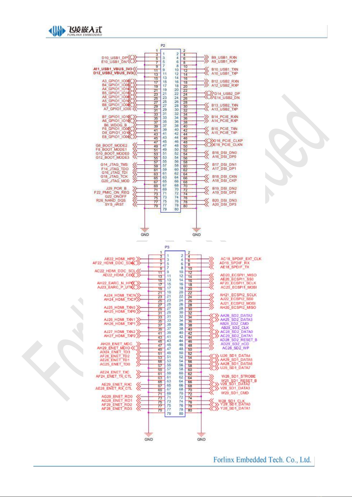
14
14
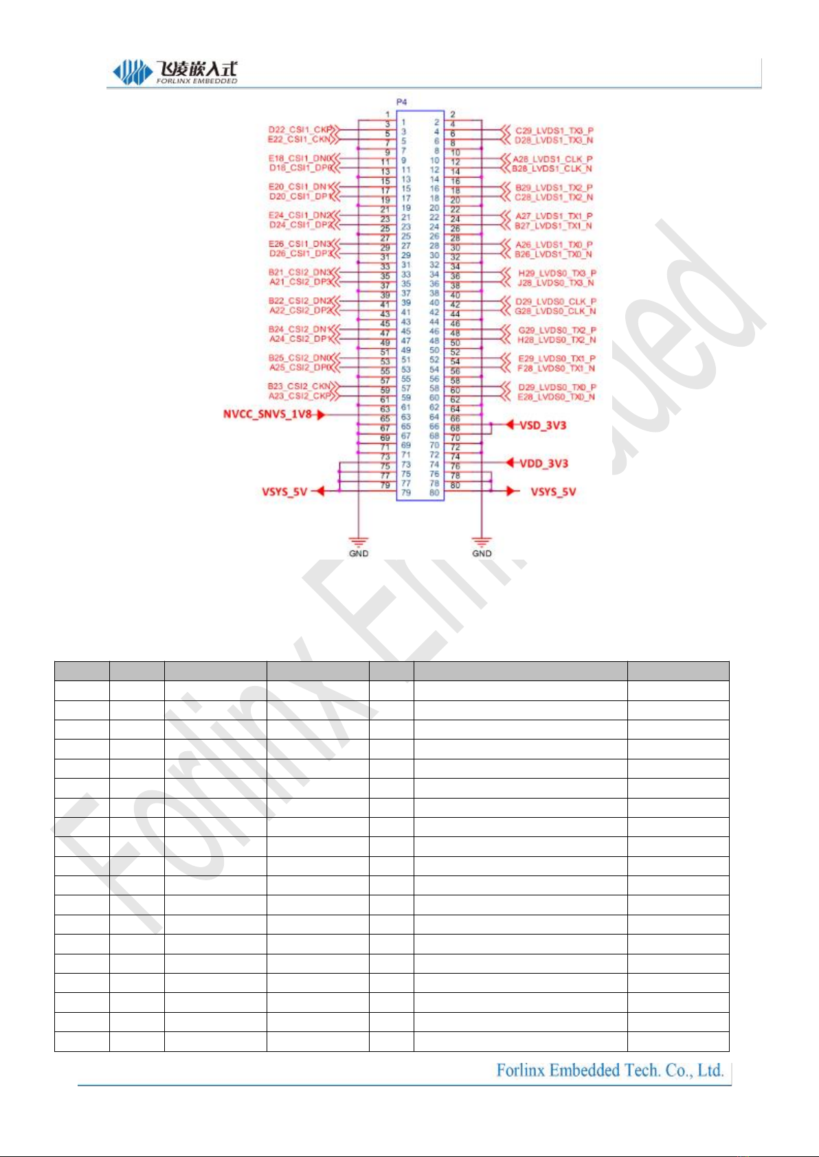
15
15
2.5.2 SoM FETMX8MPQ-C Pin Details
Table 1 LEFT_UP (P1 ) connector pins (odd)
Num
Ball
Signal
GPIO
Vol
Spec.
Default
LU_1
—
GND
—
—
GND
GND
LU_3
AH4
UART2_TXD
GPIO5_IO25
3.3V
UART2(A53 debug) data sending
UART2_TXD
LU_5
AF6
UART2_RXD
GPIO5_IO24
3.3V
UART2(A53 debug) data receiving
UART2_RXD
LU_7
AE6
UART3_RXD
GPIO5_IO26
3.3V
UART3 data receiving
UART1_CTS
LU_9
AJ4
UART3_TXD
GPIO5_IO27
3.3V
UART3 data sending
UART1_RTS
LU_11
AF8
I2C4_SCL
GPIO5_IO20
3.3V
I2C4 clock
I2C4_SCL
LU_13
AD8
I2C4_SDA
GPIO5_IO21
3.3V
I2C4 data
I2C4_SDA
LU_15
—
GND
—
—
GND
GND
LU_17
AH6
I2C2_SCL
GPIO5_IO16
3.3V
I2C2 clock
I2C2_SCL
LU_19
AE8
I2C2_SDA
GPIO5_IO17
3.3V
I2C2 data
I2C2_SDA
LU_21
AJ6
I2C3_SDA
GPIO5_IO19
3.3V
I2C3 data
I2C3_SDA
LU_23
AJ7
I2C3_SCL
GPIO5_IO18
3.3V
I2C3 clock
I2C3_SCL
LU_25
—
GND
—
—
GND
GND
LU_27
AH8
SAI1_RXC
GPIO4_IO1
1.8V
SAI1 receive bit clock
4G_RST
LU_29
AF10
SAI1_RXD1
GPIO4_IO3
1.8V
SAI1 receive data 1
5GPWR_RESE
LU_31
AC10
SAI1_RXD0
GPIO4_IO2
1.8V
SAI1 receive data 0
5GPWR_ON/O
LU_33
AJ9
SAI1_RXFS
GPIO4_IO0
1.8V
SAI1 receive frame sync
4G/5G_PWR
LU_35
—
GND
—
—
GND
GND
LU_37
AH9
SAI1_RXD2
GPIO4_IO4
1.8V
SAI1 receive data 2
ENET1_MDC

16
16
LU_39
AJ8
SAI1_RXD3
GPIO4_IO5
1.8V
SAI1 receivedata 3
ENET1_MDIO
LU_41
AD12
SAI1_TXD3
GPIO4_IO15
1.8V
SAI1 send data 3
ENET1_TD3
LU_43
AH11
SAI1_TXD2
GPIO4_IO14
1.8V
SAI1 send data 2
ENET1_TD2
LU_45
AJ10
SAI1_TXD1
GPIO4_IO13
1.8V
SAI1 send data 1
ENET1_TD1
LU_47
AJ11
SAI1_TXD0
GPIO4_IO12
1.8V
SAI1 send data 0
ENET1_TD0
LU_49
—
GND
—
—
GND
GND
LU_51
AH14
SAI1_TXD5
GPIO4_IO17
1.8V
SAI1 send data 5
ENET1_TXC
LU_53
AH13
SAI1_TXD4
GPIO4_IO16
1.8V
SAI1 send data 4
ENET1_TX_CT
LU_55
—
GND
—
—
GND
GND
LU_57
AJ12
SAI1_TXC
GPIO4_IO11
1.8V
SAI1 send bit clock
ENET1_RXC
LU_59
AF12
SAI1_TXFS
GPIO4_IO10
1.8V
SAI1 send frame sync
ENET1_RX_C
LU_61
—
GND
—
—
GND
GND
LU_63
AD10
SAI1_RXD4
GPIO4_IO6
1.8V
SAI1 receive data 4
ENET1_RD0
LU_65
AE10
SAI1_RXD5
GPIO4_IO7
1.8V
SAI1 receive data 5
ENET1_RD1
LU_67
AH10
SAI1_RXD6
GPIO4_IO8
1.8V
SAI1 receive data 6
ENET1_RD2
LU_69
AH12
SAI1_RXD7
GPIO4_IO9
1.8V
SAI1 receive data 7
ENET1_RD3
LU_71
—
GND
—
—
GND
GND
LU_73
AC12
SAI1_TXD6
GPIO4_IO18
1.8V
SAI1 send data 6
GPIO_KEY2
LU_75
AJ13
SAI1_TXD7
GPIO4_IO19
1.8V
SAI1 send data 7
CC_nINT
LU_77
AE12
SAI1_MCLK
GPIO4_IO20
1.8V
SAI1 main clock
USB1_SS_SEL
LU_79
—
GND
—
—
GND
GND
Table 2 LEFT_UP (P1 ) connector pins (even)
Num
Ball
Signal
GPIO
Vol
Spec.
Default function
LU_2
—
GND
—
—
GND
GND
LU_4
AJ3
UART1_TXD
GPIO5_IO23
3.3V
UART1 data sending
UART1_TXD
LU_6
AD6
UART1_RXD
GPIO5_IO22
3.3V
UART1 data receiving
UART1_RXD
LU_8
—
GND
—
—
GND
GND
LU_10
AH5
UART4_TXD
GPIO5_IO29
3.3V
UART4 (M7 debug)data
UART4_TXD
LU_12
AJ5
UART4_RXD
GPIO5_IO28
3.3V
UART4 (M7 debug)data
UART4_RXD
LU_14
—
GND
—
—
GND
GND
LU_16
AC14
SAI5_RXFS
GPIO3_IO19
1.8V
SAI5 receive frame sync
CSI_P2_RESET
LU_18
AD14
SAI5_RXC
GPIO3_IO20
1.8V
SAI5 receive bit clock
CSI_P2_PWDN
LU_20
AF16
SAI5_RXD2
GPIO3_IO23
1.8V
SAI5 receive data 2
HOST_WL_WA
LU_22
AD16
SAI5_RXD1
GPIO3_IO22
1.8V
SAI5 receive data 1
PCM_SYNC
LU_24
AE14
SAI5_RXD3
GPIO3_IO24
1.8V
SAI5 receive data 3
PCM_OUT
LU_26
AF14
SAI5_MCLK
GPIO3_IO25
1.8V
SAI5 main clock
PCM_CLK
LU_28
AE16
SAI5_RXD0
GPIO3_IO21
1.8V
SAI5 receive data 0
PCM_IN
LU_30
—
GND
—
—
GND
GND
LU_32
AJ16
SAI2_RXC
GPIO4_IO22
3.3V
SAI2 receive bit clock
CAN1_TX
LU_34
AH15
SAI2_TXC
GPIO4_IO25
3.3V
SAI2 send bit clock
CAN1_RX
LU_36
AH17
SAI2_RXFS
GPIO4_IO21
3.3V
SAI2 receive frame sync
SPI_INT
LU_38
AJ17
SAI2_TXFS
GPIO4_IO24
3.3V
SAI2 send frame sync
GPIO_KEY1
LU_40
AH16
SAI2_TXD
GPIO4_IO26
3.3V
SAI2 send data
CAN2_TX
LU_42
AJ15
SAI2_MCLK
GPIO4_IO27
3.3V
SAI2 main clock
CAN2_RX
LU_44
AJ14
SAI2_RXD
GPIO4_IO23
3.3V
SAI2 receive data
USB_HUB_RST
LU_46
—
GND
—
—
GND
GND
LU_48
AJ18
SAI3_RXC
GPIO4_IO29
3.3V
SAI3 receive bit clock
CODEC_PWRE
LU_50
AJ19
SAI3_RXFS
GPIO4_IO28
3.3V
SAI3 receive frame sync
AUD_nINT

17
17
LU_52
AJ20
SAI3_MCLK
GPIO5_IO2
3.3V
SAI3 main clock
SAI3_MCLK
LU_54
—
GND
—
—
GND
GND
LU_56
AH19
SAI3_TXC
GPIO5_IO0
3.3V
SAI3 send bit clock
SAI3_TXC
LU_58
AC16
SAI3_TXFS
GPIO4_IO31
3.3V
SAI3 send frame sync
SAI3_TXFS
LU_60
AH18
SAI3_TXD
GPIO5_IO1
3.3V
SAI3 send data
SAI3_TXD
LU_62
AF18
SAI3_RXD
GPIO4_IO30
3.3V
SAI3 receive data
SAI3_RXD
LU_64
—
GND
—
—
GND
GND
LU_66
K28
CLKIN1
—
3.3V
CLK input 1
CLKIN1
LU_68
—
GND
—
—
GND
GND
LU_70
K29
CLKOUT1
—
3.3V
CLK output 1
CLKOUT1
LU_72
—
GND
—
—
GND
GND
LU_74
L28
CLKIN2
—
3.3V
CLK input 2
CLKIN2
LU_76
—
GND
—
—
GND
GND
LU_78
L29
CLKOUT2
—
3.3V
CLK output 2
CLKOUT2
LU_80
—
GND
—
—
GND
GND
Table 3 RIGHT_UP (P2 )pins (odd)
Num
Ball
Signal
GPIO
Vol
Spec.
Default function
RU_1
—
GND
—
—
GND
GND
RU_3
D10
USB1_DP
—
—
USB1 data+
USB1_DP
RU_5
E10
USB1_DN
—
—
USB1 data-
USB1_DN
RU_7
—
GND
—
—
GND
GND
RU_9
A11
USB1_VBUS_3
—
3.3V
USB1_VBUS detect
USB1_VBUS_3
RU_11
D12
USB2_VBUS_3
—
3.3V
USB2_VBUS detect
USB2_VBUS_3
RU_13
—
GND
—
—
GND
GND
RU_15
A3
GPIO1_IO06
GPIO1_IO6
3.3V
GPIO
CSI1_nRST3.3
RU_17
B4
GPIO1_IO05
GPIO1_IO5
3.3V
GPIO
CSI1_SYNC3.3
RU_19
A4
GPIO1_IO14
GPIO1_IO14
3.3V
GPIO
TYPEC_HOST_
RU_21
B5
GPIO1_IO15
GPIO1_IO15
3.3V
GPIO
CSI_MCLK3.3
RU_23
A8
GPIO1_IO08
GPIO1_IO8
3.3V
GPIO
PCIE_RST
RU_25
A5
GPIO1_IO12
GPIO1_IO12
3.3V
GPIO
TP_INT
RU_27
B8
GPIO1_IO09
GPIO1_IO9
3.3V
GPIO
ACC_INT
RU_29
A7
GPIO1_IO00
GPIO1_IO0
3.3V
GPIO
LVDS_CTP_INT
RU_31
—
GND
—
—
GND
GND
RU_33
B7
GPIO1_IO10
GPIO1_IO10
3.3V
GPIO
LVDS_CTP_RS
RU_35
A6
GPIO1_IO13
GPIO1_IO13
3.3V
GPIO
LVDS_PWR_EN
RU_37
B6
WDOG_B
GPIO1_IO2
3.3V
watchdog
WDOG_B
RU_39
F6
GPIO1_IO07
GPIO1_IO7
3.3V
GPIO
DSI_EN
RU_41
D8
GPIO1_IO11
GPIO1_IO11
3.3V
GPIO
LVDS_PWM
RU_43
E8
GPIO1_IO01
GPIO1_IO1
3.3V
GPIO
DSI_BL_PWM
RU_45
—
GND
—
—
GND
GND
RU_47
G8
BOOT_MODE2
—
3.3V
BOOT booting mode select
BOOT_MODE2
RU_49
F8
BOOT_MODE1
—
3.3V
BOOT booting mode select
BOOT_MODE1
RU_51
G10
BOOT_MODE0
—
3.3V
BOOT booting mode select
BOOT_MODE0
RU_53
G12
BOOT_MODE3
—
3.3V
BOOT booting mode select
BOOT_MODE3
RU_55
—
GND
—
—
GND
GND
RU_57
G14
JTAG_TMS
—
3.3V
JTAG test mode select
JTAG_TMS
RU_59
F14
JTAG_TDO
—
3.3V
JTAG test data serial output
JTAG_TDO
RU_61
G16
JTAG_TDI
—
3.3V
JTAG test data serial input
JTAG_TDI
RU_63
G18
JTAG_TCK
—
3.3V
JTAG detect clock
JTAG_TCK

18
18
RU_65
G20
JTAG_MOD
—
3.3V
JTAG mode select
JTAG_MOD
RU_67
—
GND
—
—
GND
GND
RU_69
J29
POR_B
—
1.8V
CPU reset
POR_B
RU_71
F22
PMIC_ON_REQ
—
1.8V
PMIC power supply request
PMIC_ON_REQ
RU_73
G22
ONOFF
—
1.8V
power on/ off signal
ONOFF
RU_75
R26
NAND_DQS
GPIO3_IO14
1.8V
NAND_DQS clock
NAND_DQS
Do not used for carrier board
RU_77
—
SYS_NRST
—
1.8V
SoM power reset
SYS_NRST
RU_79
—
GND
—
—
GND
GND
Table 4 RIGHT (P2) (even)
Num
Ball
Signal
GPIO
Vol
Spec.
Default function
RU_2
—
GND
—
—
GND
GND
RU_4
B9
USB1_RXN
—
—
USB1 receive-
USB1_RXN
RU_6
A9
USB1_RXP
—
—
USB1 receive+
USB1_RXP
RU_8
—
GND
—
—
GND
GND
RU_10
B10
USB1_TXN
—
—
USB1 send-
USB1_TXN
RU_12
A10
USB1_TXP
—
—
USB1 send+
USB1_TXP
RU_14
—
GND
—
—
GND
GND
RU_16
B12
USB2_RXN
—
—
USB2 receive-
USB2_RXN
RU_18
A12
USB2_RXP
—
—
USB2 receive+
USB2_RXP
RU_20
—
GND
—
—
GND
GND
RU_22
D14
USB2_DP
—
—
USB2 data+
USB2_DP
RU_24
E14
USB2_DN
—
—
USB2 data-
USB2_DN
RU_26
—
GND
—
—
GND
GND
RU_28
B13
USB2_TXN
—
—
USB2 send-
USB2_TXN
RU_30
A13
USB2_TXP
—
—
USB2 send+
USB2_TXP
RU_32
—
GND
—
—
GND
GND
RU_34
B14
PCIE_RXN
—
—
PCIE data receive-
PCIE_RXN
RU_36
A14
PCIE_RXP
—
—
PCIE data receive+
PCIE_RXP
RU_38
—
GND
—
—
GND
GND
RU_40
B15
PCIE_TXN
—
—
PCIE data send-
PCIE_TXN
RU_42
A15
PCIE_TXP
—
—
PCIE data send+
PCIE_TXP
RU_44
—
GND
—
—
GND
GND
RU_46
D16
PCIE_CLKP
—
—
PCIE clock input+
PCIE_CLKP
RU_48
E16
PCIE_CLKN
—
—
PCIE clock input-
PCIE_CLKN
RU_50
—
GND
—
—
GND
GND
RU_52
B16
DSI_DN0
—
—
DSI data 0-
DSI_DN0
RU_54
A16
DSI_DP0
—
—
DSI data 0+
DSI_DP0
RU_56
—
GND
—
—
GND
GND
RU_58
B17
DSI_DN1
—
—
DSI data 1-
DSI_DN1
RU_60
A17
DSI_DP1
—
—
DSI data 1+
DSI_DP1
RU_62
—
GND
—
—
GND
GND
RU_64
B18
DSI_CKN
—
—
DSI clock -
DSI_CKN
RU_66
A18
DSI_CKP
—
—
DSI clock +
DSI_CKP
RU_68
—
GND
—
—
GND
GND
RU_70
B19
DSI_DN2
—
—
DSI data 2-
DSI_DN2
RU_72
A19
DSI_DP2
—
—
DSI data 2+
DSI_DP2
RU_74
—
GND
—
—
GND
GND
RU_76
B20
DSI_DN3
—
—
DSI data 3-
DSI_DN3
19
19
RU_78
A20
DSI_DP3
—
—
DSI data 3+
DSI_DP3
RU_80
—
GND
—
—
GND
GND
Table 5 LEFT_DOWN (P3 ) (odd)
Num
Ball
Signal
GPIO
Vol
Spec.
Default function
LD_1
—
GND
—
—
GND
GND
LD_3
AE22
HDMI_HPD
GPIO3_IO29
3.3V
HDMI hot plug detect
HDMI_HPD
LD_5
AF22
HDMI_DDC_SDA
GPIO3_IO27
3.3V
HDMI_DDC data
HDMI_DDC_SD
LD_7
—
GND
—
—
GND
GND
LD_9
AC22
HDMI_DDC_SCL
GPIO3_IO26
3.3V
HDMI_DDC clock
HDMI_DDC_SC
LD_11
AD22
HDMI_CEC
GPIO3_IO28
3.3V
HDMI_CEC recognize
HDMI_CEC
LD_13
—
GND
—
—
GND
GND
LD_15
AH22
EARC_N_HPD
—
—
eARC differential -
EARC_N_HPD
LD_17
AJ23
EARC_P_UTIL
—
—
eARC differential +
EARC_P_UTIL
LD_19
—
GND
—
—
GND
GND
LD_21
AJ24
HDMI_TXCN
—
—
HDMI differential clock-
HDMI_TXCN
LD_23
AH24
HDMI_TXCP
—
—
HDMI differential clock+
HDMI_TXCP
LD_25
—
GND
—
—
GND
GND
LD_27
AJ25
HDMI_TXN0
—
—
HDMI differential data 0-
HDMI_TXN0
LD_29
AH25
HDMI_TXP0
—
—
HDMI differential data 0+
HDMI_TXP0
LD_31
—
GND
—
—
GND
GND
LD_33
AJ26
HDMI_TXN1
—
—
HDMI differential data 1-
HDMI_TXN1
LD_35
AH26
HDMI_TXP1
—
—
HDMI differential data 1+
HDMI_TXP1
LD_37
—
GND
—
—
GND
GND
LD_39
AJ27
HDMI_TXN2
—
—
HDMI differential data 2-
HDMI_TXN2
LD_41
AH27
HDMI_TXP2
—
—
HDMI differential data 2+
HDMI_TXP2
LD_43
—
GND
—
—
GND
GND
LD_45
AH28
ENET_MDC
GPIO1_IO16
1.8V
ENET serial management clock
ENET_MDC
LD_47
AH29
ENET_MDIO
GPIO1_IO17
1.8V
ENET serial management data
ENET_MDIO
LD_49
AD24
ENET_TD3
GPIO1_IO18
1.8V
RGMII data send 3
ENET_TD3
LD_51
AF26
ENET_TD2
GPIO1_IO19
1.8V
RGMII data send 2
ENET_TD2
LD_53
AE26
ENET_TD1
GPIO1_IO20
1.8V
RGMII data send 1
ENET_TD1
LD_55
AC25
ENET_TD0
GPIO1_IO21
1.8V
RGMII data send 0
ENET_TD0
LD_57
—
GND
—
—
GND
GND
LD_59
AE24
ENET_TXC
GPIO1_IO23
1.8V
RGMII send clock
ENET_TXC
LD_61
AF24
ENET_TX_CTL
GPIO1_IO22
1.8V
RGMII send control
ENET_TX_CTL
LD_63
—
GND
—
—
GND
GND
LD_65
AE29
ENET_RXC
GPIO1_IO25
1.8V
RGMII receive clock
ENET_RXC
LD_67
AE28
ENET_RX_CTL
GPIO1_IO24
1.8V
RGMII receive control
ENET_RX_CTL
LD_69
—
GND
—
—
GND
GND
LD_71
AG29
ENET_RD0
GPIO1_IO26
1.8V
RGMII receive data 0
ENET_RD0
LD_73
AG28
ENET_RD1
GPIO1_IO27
1.8V
RGMII receive data 1
ENET_RD1
LD_75
AF29
ENET_RD2
GPIO1_IO28
1.8V
RGMII receive data 2
ENET_RD2
LD_77
AF28
ENET_RD3
GPIO1_IO29
1.8V
RGMII receive data 3
ENET_RD3
LD_79
—
GND
—
—
GND
GND

20
20
Table 6 LEFT_DOWN (P3) (even)
Num
Ball
Signal
GPIO
Vol
Spec.
Default function
LD_2
—
GND
—
—
GND
GND
LD_4
AC18
SPDIF_EXT_CL
GPIO5_IO5
3.3V
SPDIF clock
ENET_nRST
LD_6
AD18
SPDIF_RX
GPIO5_IO4
3.3V
SPDIF receive
ENET1_nRST
LD_8
AE18
SPDIF_TX
GPIO5_IO3
3.3V
SPDIF send
ENET_nINT
LD_10
—
GND
—
—
GND
GND
LD_12
AD20
ECSPI1_MISO
GPIO5_IO8
3.3V
ECSPI1 host input slave output
GPIO_LED1
LD_14
AE20
ECSPI1_SS0
GPIO5_IO9
3.3V
ECSPI1 chip select
GPIO_LED2
LD_16
AF20
ECSPI1_SCLK
GPIO5_IO6
3.3V
ECSPI1 clock
UART3_RXD
LD_18
AC20
ECSPI1_MOSI
GPIO5_IO7
3.3V
ECSPI1 host output slave input
UART3_TXD
LD_20
—
GND
—
—
GND
GND
LD_22
AH21
ECSPI2_SCLK
GPIO5_IO10
3.3V
ECSPI2 clock
ECSPI2_SCLK
LD_24
AJ22
ECSPI2_SS0
GPIO5_IO13
3.3V
ECSPI2 chip select
ECSPI2_SS0
LD_26
AJ21
ECSPI2_MOSI
GPIO5_IO11
3.3V
ECSPI2 host output slave input
ECSPI2_MOSI
LD_28
AH20
ECSPI2_MISO
GPIO5_IO12
3.3V
ECSPI2 host input slave output
ECSPI2_MISO
LD_30
—
GND
—
—
GND
GND
LD_32
AA26
SD2_DATA2
GPIO2_IO17
1.8/3.3
SD2 data bit 2
SD2_DATA2
LD_34
AA25
SD2_DATA3
GPIO2_IO18
1.8/3.3
SD2 data bit 3
SD2_DATA3
LD_36
AB28
SD2_CMD
GPIO2_IO14
1.8/3.3
SD2 command signal
SD2_CMD
LD_38
AB29
SD2_CLK
GPIO2_IO13
1.8/3.3
SD2 clock
SD2_CLK
LD_40
AC28
SD2_DATA0
GPIO2_IO15
1.8/3.3
SD2 data bit 0
SD2_DATA0
LD_42
AC29
SD2_DATA1
GPIO2_IO16
1.8/3.3
SD2 data bit 1
SD2_DATA1
LD_44
AD28
SD2_RESET_B
GPIO2_IO19
1.8/3.3
SD2 reset signal
Carrier board not use
LD_46
AD29
SD2_NCD
GPIO2_IO12
1.8/3.3
SD2 card detect signal
SD2_nCD
LD_48
AC26
SD2_WP
GPIO2_IO20
1.8/3.3
SD2 write protect signal
TYPEC_EN_B
LD_50
—
GND
—
—
GND
GND
LD_52
U26
SD1_DATA4
GPIO2_IO6
1.8V
SD1 data bit 4
BT_HOST_WAKE
LD_54
AA29
SD1_DATA5
GPIO2_IO7
1.8V
SD1 data bit 5
BT_WAKE_B
LD_56
AA28
SD1_DATA6
GPIO2_IO8
1.8V
SD1 data bit 6
WIFI_REG_ON
LD_58
U25
SD1_DATA7
GPIO2_IO9
1.8V
SD1 data bit 7
WIFI_HOST_WAK
LD_60
—
GND
—
—
GND
GND
LD_62
W26
SD1_STROBE
GPIO2_IO11
1.8V
SD1 strobe signal
CSI1_PWDN
LD_64
W25
SD1_RESET_B
GPIO2_IO10
1.8V
SD1 reset signal
BT_REG_ON
LD_66
V29
SD1_DATA2
GPIO2_IO4
1.8V
SD1 data bit 2
SD1_DATA2
LD_68
V28
SD1_DATA3
GPIO2_IO5
1.8V
SD1 data bit 3
SD1_DATA3
LD_70
W29
SD1_CMD
GPIO2_IO1
1.8V
SD1 command signal
SD1_CMD
LD_72
—
GND
—
—
GND
GND
LD_74
W28
SD1_CLK
GPIO2_IO0
1.8V
SD1 clock
SD1_CLK
LD_76
Y29
SD1_DATA0
GPIO2_IO2
1.8V
SD1 data bit 0
SD1_DATA0
LD_78
Y28
SD1_DATA1
GPIO2_IO3
1.8V
SD1 data bit 1
SD1_DATA1
LD_80
—
GND
—
—
GND
GND
This manual suits for next models
1
Table of contents
Other Forlinx Motherboard manuals


