Goodix GR5515 User manual

GR5515 Starter Kit User Guide
Version: 1.5
Release Date: 2020-05-30
Shenzhen Goodix Technology Co., Ltd.

Copyright © 2020 Shenzhen Goodix Technology Co., Ltd. All rights reserved.
Any excerption, backup, modification, translation, transmission or commercial use of this document or any portion
of this document, in any form or by any means, without the prior written consent of Shenzhen Goodix Technology
Co., Ltd is prohibited.
Trademarks and Permissions
and other Goodix trademarks are trademarks of Shenzhen Goodix Technology Co., Ltd. All other
trademarks and trade names mentioned in this document are the property of their respective holders.
Disclaimer
Information contained in this document is intended for your convenience only and is subject to change without
prior notice. It is your responsibility to ensure its application complies with technical specifications.
Shenzhen Goodix Technology Co., Ltd. (hereafter referred to as “Goodix”) makes no representation or guarantee
for this information, express or implied, oral or written, statutory or otherwise, including but not limited to
representation or guarantee for its application, quality, performance, merchantability or fitness for a particular
purpose. Goodix shall assume no responsibility for this information and relevant consequences arising out of the
use of such information.
Without written consent of Goodix, it is prohibited to use Goodix products as critical components in any life
support system. Under the protection of Goodix intellectual property rights, no license may be transferred
implicitly or by any other means.
Shenzhen Goodix Technology Co., Ltd.
Headquarters: 2F. & 13F., Tower B, Tengfei Industrial Building, Futian Free Trade Zone, Shenzhen, China
TEL: +86-755-33338828 FAX: +86-755-33338830
Website: www.goodix.com

Preface
Copyright © 2020 Shenzhen Goodix Technology Co., Ltd. I
Preface
Purpose
This document introduces the GR5515 Starter Kit (GR5515 SK), the hardware layout, the circuit schematics,
hardware functional modules, and RF and current tests of the GR5515 Starter Kit Board (GR5515 SK Board), to
help you get started with the GR5515 Starter Kit Board quickly in developing Bluetooth Low Energy (Bluetooth LE)
products and applications with GR551x System on Chips (SoCs).
Audience
This document is intended for:
•GR551x user
•GR551x developer
•GR551x tester
•Technical writer
Release Notes
This document is the third release of GR5515 Starter Kit User Guide, corresponding to GR551x_SDK_V1.5.0.
Revision History
Version
Date
Description
1.0
2019-12-08
Initial release
1.3
2020-03-16
Updated the release time in the footers.
1.5
2020-05-30
Optimized the descriptions in “Chapter 9 On-board QSPI Flash”.

Contents
Copyright © 2020 Shenzhen Goodix Technology Co., Ltd. II
Contents
Preface.............................................................................................................................................................I
1 Introduction .................................................................................................................................................1
1.1 Characteristics ...................................................................................................................................................1
2 Quick Start Guide..........................................................................................................................................1
2.1 Preparation........................................................................................................................................................1
2.2 Power Supply and Connection Settings.............................................................................................................1
2.3 Example Running...............................................................................................................................................2
2.4 Mobile Connection Test.....................................................................................................................................2
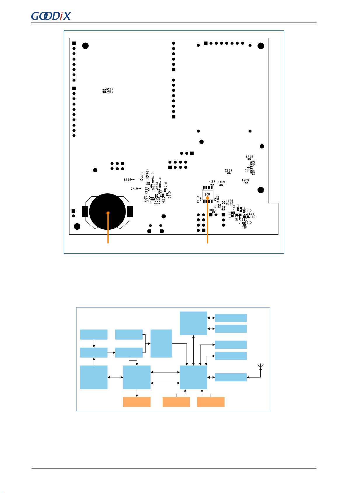
3 Hardware Overview......................................................................................................................................3
3.1 Hardware Layout ...............................................................................................................................................3
3.2 Block Diagram....................................................................................................................................................4
4 Interface MCU ..............................................................................................................................................5
4.1 J-Link Port ..........................................................................................................................................................5
4.2 CDC Virtual Serial Port.......................................................................................................................................5
4.3 Software Download Port of Interface MCU.......................................................................................................5
5 Power Supply ...............................................................................................................................................6
6 Arduino Uno Shield Connectors.....................................................................................................................9
7 Buttons and LEDs........................................................................................................................................ 10
8 LCD Connector............................................................................................................................................ 11
9 On-board QSPI Flash...................................................................................................................................12
10 Performance Test...................................................................................................................................... 13
10.1 RF Test............................................................................................................................................................13
10.2 Current Consumption Test.............................................................................................................................14

Introduction
Copyright © 2020 Shenzhen Goodix Technology Co., Ltd. 1
1 Introduction
The GR5515 SK is a development platform based on GR551x SoCs (supporting Bluetooth 5.1). It contains a GR5515
SK Board, a schematic diagram, and a user guide. The GR5515 SK allows you to get familiar with GR551x-related
development tools, quickly develop product prototype, and verify related functions.
Figure 1-1 GR5515 SK Board
By default, no software is pre-downloaded on a GR5515 SK Board. It is recommended to download the Bluetooth
or peripheral application example projects provided in a GR551x SDK to a GR5515 SK Board for development and
debugging.
To make best use of the GR5515 SK, it is recommended to refer to the following documents.
Table 1-1 Reference documents
Name
Description
GR551x Developer Guide
Introduces the software/hardware and quick start guide of GR551x SoCs.
J-Link/J-Trace User Guide
Provides J-Link operational instructions. Available at
https://www.segger.com/downloads/jlink/UM08001_JLink.pdf.
GR5515-SK-BASIC-RevC
Offers GR5515 Starter Kit Board schematic diagrams.
1.1 Characteristics
•A single-mode Bluetooth LE SoC that supports Bluetooth 5.1
•Multi-functional buttons and LEDs
•Interfaces that support inserting the Arduino module, with I/O voltage configurable by level shift

Introduction
Copyright © 2020 Shenzhen Goodix Technology Co., Ltd. 2
•SEGGER J-Link OB that supports debugging
•UART-to-USB connector
•Micro USB connector, which establishes connection between a GR5515 SK Board and a PC
•1.44-inch color TFT display
•On-board QSPI flash

Quick Start Guide
Copyright © 2020 Shenzhen Goodix Technology Co., Ltd. 1
2 Quick Start Guide
2.1 Preparation
Perform the following tasks before getting started with a GR5515 SK Board.
Note:
SDK_Folder is the root directory of GR551x SDK.
•Hardware preparation
Table 2-1 Hardware preparation
Name
Description
Cable
Micro USB 2.0 cable
Development board
GR5515 Starter Kit Board
•Software preparation
Table 2-2 Software preparation
Name
Description
Windows
Windows 7 or later versions, or Ubuntu 16.04 LTS or later versions (both 32-bit and 64-bit are
acceptable)
Keil MDK5
An integrated development environment (IDE). Available at http://www.keil.com/download/product/.
GRToolbox (Android)
A Bluetooth LE debugging tool for GR551x. Available in SDK_Folder\tools\GRToolbox.
2.2 Power Supply and Connection Settings
Figure 2-1 shows the assembly diagram of a GR5515 SK Board.
LCD
Arduino
S6
S5
D102
Micro USB Connector(J49)iPex Connector
Printed
Antenna
Figure 2-1 GR5515 SK Board assembly
Before using a GR5515 SK Board, follow the steps below to configure power supply and establish connection:

Quick Start Guide
Copyright © 2020 Shenzhen Goodix Technology Co., Ltd. 2
1. Connect the GR5515 SK Board to a PC with a Micro USB 2.0 cable. The Micro USB connector is used for power
supply and programming through J-Link.
2. Switch S6 (power switch) to the right side (as shown in the figure above) to power the board with current
passing through the on-board LDO; switch S6 to the left side to power the board by lithium batteries.
3. Switch S5 (power switch) to the right side (marked with ON) to turn on the power.
4. D102 starting flashing indicates that the PC begins to detect the J-Link port. If the detection succeeds, D102
stops flashing and remains on.
5. When D102 remains on, open the File Explorer of the PC, and check whether J-Link is in the list of Device
Manager > Ports (COM & LPT). J-Link in the list indicates that power and connection settings are completed,
and downloading and programming for GR551x are permitted; otherwise, check whether the J-Link driver is
installed properly, and reinstall the J-Link driver in the latest version if necessary.
2.3 Example Running
The GR551x SDK provides various example projects, which are in SDK_Folder\projects. After completing
power supply and connection settings, you can run any example project. For more information about compiling
and downloading example projects with Keil, see the GR551x Developer Guide.
2.4 Mobile Connection Test
Install GRToolbox App on a mobile phone (Android), and enable Bluetooth on the phone. Run the GRToolbox to
start scanning and establish connection with the GR5515 SK Board.

Hardware Overview
Copyright © 2020 Shenzhen Goodix Technology Co., Ltd. 3
3 Hardware Overview
3.1 Hardware Layout
The top view and the bottom view of a GR5515 SK Board are shown in Figure 3-1 and Figure 3-2 respectively. The
board mainly integrates an interface microcontroller unit (MCU), a power module, Arduino Uno Shield Connectors,
buttons and LEDs, a LCD connector, a Bluetooth LE RF module, and an on-board QSPI flash.
Power module Interface MCU Buttons and LEDs Bluetooth LE RF
module
Arduino Uno Shield Connectors Arduino Uno Shield Connectors LCD connector
Figure 3-1 Hardware layout of GR5515 SK Board (top view)

Hardware Overview
Copyright © 2020 Shenzhen Goodix Technology Co., Ltd. 4
Lithium battery On-board QSPI Flash
Figure 3-2 Hardware layout of GR5515 SK Board (bottom view)
3.2 Block Diagram
The following block diagram of a GR5515 SK Board shows connections between modules.
External supply
Power
Switch (S5)
Battery
LDO (1.8 V,3.3 V)
USB
POWER +5 V
Communication
Interface MCU GR5515
Level shift
Power
Switch (S6)
J-LINK Osc.
32.768 kHz OSC. 32 MHz
LEDs
Buttons
Matching network
GPIO/Arduino Uno
LCD
Antenna
Data
5 V
3.3V
SWD
UART
Figure 3-3 Block diagram of GR5515 SK Board

Interface MCU
Copyright © 2020 Shenzhen Goodix Technology Co., Ltd. 5
4 Interface MCU
The board integrates an Atmel interface MCU, which can be converted to a J-Link port and a CDC virtual serial
port.
4.1 J-Link Port
The GR5515 SK Board integrates a J-Link OB chip, which allows you to perform online debugging and emulation
with the J-Link driver of the PC.
4.2 CDC Virtual Serial Port
J-Link OB chip internally integrates CDC serial protocols, which allow you to open the J-Link CDC virtual serial port
on the PC, to debug with UART.
Table 4-1 Relationship between UART connectors and interface MCU
GR5515 SK Board
Interface MCU
Default GPIO
UART
UART
GPIO10
RX
TX
GPIO11
TX
RX
4.3 Software Download Port of Interface MCU
The J-Link port, J43, on the GR5515 SK Board is used for SEGGER J-Link OB firmware download for interface MCU.
Note:
GR5515 SK Boards have been factory-programmed with J-Link OB firmware. No programming is required for users.

Power Supply
Copyright © 2020 Shenzhen Goodix Technology Co., Ltd. 6
5 Power Supply
The GR5515 SK Board provides three power supply modes: power supply via USB connection, power supply from
external sources and from lithium battery.
Power supply via USB
connection
Power supply from
external sources
Figure 5-1 Power supply (top view)

Power Supply
Copyright © 2020 Shenzhen Goodix Technology Co., Ltd. 7
Power supply from lithium battery
Figure 5-2 Power supply (bottom view)
•Power supply via USB connection: Power the board by connecting the board to the PC with a USB cable with
current passing through the on-board LDO. The LDO output voltage ranges from 1.8 V to 3.3 V; default: 3.3 V.
•Power supply from external sources: Power the board by external sources (5 V) with current passing through
the on-board LDO. The default LDO output voltage is 3.3 V.
•Power supply from lithium battery: Power the board by lithium batteries.
You can switch S6, to select the power supply mode (from lithium battery or the 3.3 V power output by the
on-board LDO). Reverse voltage protection is provided for power supply via USB connection and from external
sources through a pair of diodes (D100 and D105).

Power Supply
Copyright © 2020 Shenzhen Goodix Technology Co., Ltd. 8
Figure 5-3 Voltage protection diodes for power supply via USB connection/from external sources

Arduino Uno Shield Connectors
Copyright © 2020 Shenzhen Goodix Technology Co., Ltd. 9
6 Arduino Uno Shield Connectors
The GR5515 SK Board provides standard Arduino Uno Shield Connectors, and the connector locations on the SK
printed circuit board (PCB) comply with Arduino standards. You can connect peripherals, such as G-sensor and
heart rate sensor, through Arduino Uno Shield Connectors.
Figure 6-1 Arduino Uno Shield Connectors on GR5515 SK Board
The I/O voltage of Arduino Uno Shield Connectors can be set to 1.8 V, 3.3 V, or 5 V by using a jumper cap on J65.
Figure 6-2 Voltage options of Arduino Uno Shield Connectors
Note:
GPIO6 and GPIO7 are shared by D0/RX, D1/TX, and LCD display interface in Time-Division Multiplexing (TDM). For
more information about GR5515 SK Board circuit, see the schematic diagram GR5515-SK-BASIC-RevC.

Buttons and LEDs
Copyright © 2020 Shenzhen Goodix Technology Co., Ltd. 10
7 Buttons and LEDs
The GR5515 SK Board integrates 6 buttons and 3 LEDs, with corresponding GR551x pins as follows:
Table 7-1 Corresponding pins to buttons/LEDs
Button/LED
GPIO Pin
Description
Note
Button1
GPIO14
S3 (LEFT)
-
Button2
GPIO15
S4 (RIGHT)
-
Button3
GPIO12
S1 (UP)
-
Button4
GPIO13
S2 (DOWN)
-
Button5
AON_GPIO1
S8 (OK)
AON_GPIO1. It can be configured to wake the system
up from sleep mode in application, just like the PCS
project in SDK.
Button6
CHIP_EN
S7 (RESET)
It is used for chip reset.
LED1
MSIO4
D104 (PWM controllable)
LED1 can be driven by different PWM modes.
LED2
GPIO4
D106 (user-defined)
-
LED3
D102 (J-Link status indicator)
It is connected to interface MCU to indicate J-Link
status. When it is powered on, it flashes; if J-Link
driver on the PC is ready, it remains on.

LCD Connector
Copyright © 2020 Shenzhen Goodix Technology Co., Ltd. 11
8 LCD Connector
The GR5515 SK Board integrates a color TFT LCD display (1.44 inch, 128 x 128 dpi) and a 3-wire serial peripheral
interface (SPI), to help you develop and demonstrate products with display function. In addition, the LCD display is
pluggable. You can replace it with different-size displays supporting the same type of connection interfaces, to
adapt to different application scenarios.
Figure 8-1 Interface network of the LCD connector
Table 8-1 Pin definition of LCD connector
Pin
NET
Description
1
GND
Ground
2
VCC
+3.3 V
3
SCL/CLK
SPI clock input
4
SDA/MOSI
SPI data input
5
RES
Display reset
6
DC
Data/Command selection
7
CS
Chip selection for SPI
8
BLK
Backlight control input

On-board QSPI Flash
Copyright © 2020 Shenzhen Goodix Technology Co., Ltd. 12
9 On-board QSPI Flash
The GR5515 SK Board integrates a 32 MB QSPI flash, to expand flash memory and store application data.
Figure 9-1 Expanded QSPI flash schematic diagram
Note:
•QSPI flash pins, buttons (UP, LEFT, RIGHT, DOWN), and Arduino Uno Shield Connectors pins (GPIO8 and GPIO9)
multiplex. By default, the zero-ohm resistor is disconnected, and QSPI flash pins do not work.
•To use QSPI flash pins, disconnect these pins from buttons, GPIO8, and GPIO9, and solder a zero-ohm resistor
at the corresponding DNI resistance part.
Figure 9-2 Connections shared by buttons and QSPI flash pins

Performance Test
Copyright © 2020 Shenzhen Goodix Technology Co., Ltd. 13
10 Performance Test
10.1 RF Test
The GR5515 SK Board reserves a small RF connector (J50), which can be connected to a spectrum analyzer or a
Bluetooth LE tester (for example, TLF3000) to test the RF performance of the GR5515 SK Board.
The RF connector, J50, integrates an internal switch:
•By default, if no test line probe is connected to J50, the RF circuit signal is connected to on-board antenna.
•If any test line probe is connected to J50, the RF circuit signal is directly connected with the test line, not the
board-level antenna any more. The other end of the test line is connected to a test instrument through a
standard SMA connector.
Note:
It is recommended to use a high-frequency test line, such as MURATA MXHS83QE3000, to test RF performance for
the GR5515 SK Board; the test probe is not included in the GR5515 SK package.
Figure 10-1 shows test connection between a GR5515 SK Board and TLF3000 by taking TLF3000 as an example.
Micro USB Cable
Micro USB Cable
Cable
Back
Figure 10-1 Connection between GR5515 SK Board and TLF3000
After establishing connection, you can select different test items from the software on the PC, to test RF-related
parameters.

Performance Test
Copyright © 2020 Shenzhen Goodix Technology Co., Ltd. 14
Figure 10-2 RF parameter test demo
Note:
For more information about RF tests, see the GR551x DTM Test Application Note.
10.2 Current Consumption Test
You can test the current consumption of the GR551x SoC on the GR5515 SK Board with a test instrument. On the
board, VBAT powers VBATH, VBATL, and VBAT-RF of the GR551x SoC through the jumper pin J10. Therefore, you
can connect a test instrument to J10 to test the current.
Figure 10-3 Current consumption test interface J10
Current test instruments include a multimeter, an oscilloscope, and a power analyzer.
•Multimeter
A multimeter is used to test static current or average current.
Table of contents