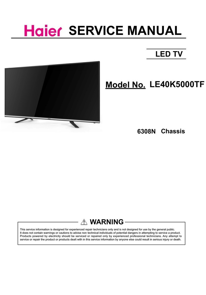
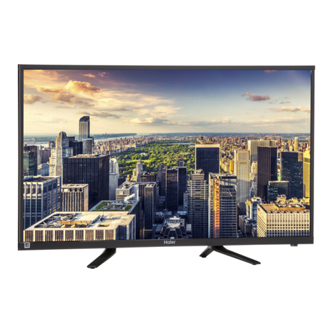
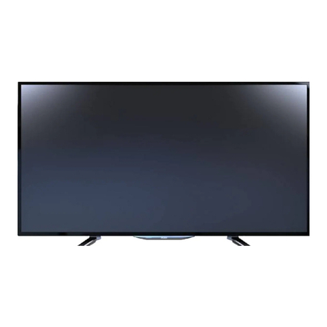
Haier LE42H6600CU User manual

SERVICE MANUAL
LED TV
Model No. LE42H6600CU
Chassis
MSD308
This service information is designed for experienced repair technicians only and is not designed for use by the general public.
It does not contain warnings or cautions to advise non-technical individuals of potential dangers in attempting to service a product.
Products powered by electricity should be serviced or repaired only by experienced professional technicians. Any attempt to service or repair
the product or products dealt with in this service information by anyone else could result in serious injury or death.
Haier Group
©2011 Qingdao Haier Electronics Co., Ltd.
All rights reserved. Unauthorized copying and distribution is a violation of law.
WARNING

1-1. Table of Contents
1. General Information
1-2. Important Notice
3
Chapter 1: General Information
1
3
1-1. General Guidelines
1-3. How to Read this Service Manual 6
....................................................................................
Service Manual
Model No.:
- 01 -
3. Location of Controls and Components
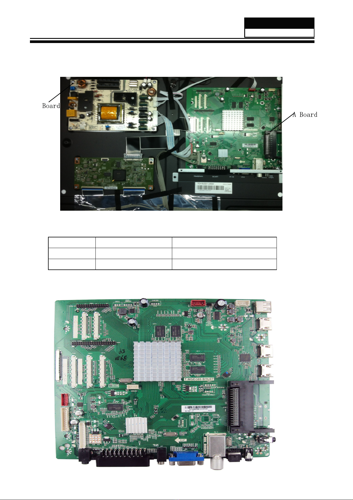
3-1. Board Location
3-2. Main Board
3-3. Power Board
3-4. LCD Panel
4. Disassemble and Assemble .......................................................
7
8
8
8
14
15
17
5. Electrical Parts ....………………...........…………......................... 22
6. Trouble-shooting ……….............................................................. 23
2. Specification
.........................................
......................................................................
7. Hotel Mode ……….............................................................. 34
8. Upgrade Instruction ….............................................................. 35

Service Manual
Model No.:
- 02 -

8VHWKHJHQHZLQJSDUWVVSHFL¿HGSDUWV
1-1. General Guidelines
When servicing, observe the original lead dress. Ifashort circuit is found, replace all parts
which have been overheated or damaged by the short circuit.
After servicing, see to it that all the protective devices such as insulation barriers, insulation
papers shields are properly installed.
After servicing, make the followingleakage current checks to prevent the customer from
beingexposed to shock hazards.
1) Leakage Current Cold Check
2) Leakage Current Hot Check
3) Prevention ofElectro Static Discharge (ESD) to Electrostatically Sensitive
1-2. Important Notice
1-2-1. Followthe regulations and warnings
Most important thingis to list up the potential hazard or risk for the service personnel to
open the units and disassemble the units. For example, we need to describe properly
howto avoid the possibility to get electrical shock fromthe live power supply or charged
electrical parts (even the power is off).
This symbol indicates that high voltage is present inside.It is dangerous to
make any kingofcontact with any inside part ofthis product.
This symbol indicates that there are important operatingand maintenance
instructions in the literture accompanyingthe appliance.
1-2-2. Be careful to the electrical shock
7RSUHYHQWGDPDJHZKLFKPLJKWUHVXOWLQHOHFWULFVKRFNRU¿UHGRQRWH[SRVHWKLV79VHW
to rain or excessive moisture. This TV must not be exposed to drippingor splashingwater,
DQGREMHFWV¿OOHGZLWKOLTXLGVXFKDVYDVHVPXVWQRWEHSODFHGRQWRSRIRUDERYHWKH79
1-2-3. Electro static discharge (ESD)
Some semiconductor (solid state) devices can be damaged easily by static electricity. Such
components commonly are called Electrostatically Sensitive (ES) Devices. The following
techniques should be used to help reduce the incidence ofcomponent damage caused by
1-2-4. About lead free solder (PbF)1-2-4. About lead free solder (PbF)
This product is manufactured usinglead-free solder as apart ofamovement within the
consumer products industry at large to be environmentally responsible. Lead-free solder
Special parts which have purposes offire retardant (resistors), high-quality sound
(capacitors), lownoise (resistors), etc. are used.
When replacingany ofcomponents, be sure to use only manufacture's specified parts
shown in the parts list.
Safety Component
Ɣ&RPSRQHQWVLGHQWL¿HGE\PDUNKDYHVSHFLDOFKDUDFWHULVWLFVLPSRUWDQWIRUVDIHW\
Service Manual
Model No.:
- 03-
1-2-5.

1-2-6Safety Check after Repairment
- 04 -
Service Manual
Model No.:
&RQ¿UPWKDWWKHVFUHZVSDUWVDQGZLULQJZKLFKZHUHUHPRYHGLQRUGHUWRVHUYLFHDUHSXW
in the original positions, or whether there are the positions which are deteriorated around
the serviced places serviced or not. Check the insulation between the antennaterminal or
external metal and the AC cord plugblades. And be sure the safety ofthat.
General ServicingPrecautions
1. Always unplugthe receiver AC power cord fromthe AC power source before;
a. Removingor reinstallingany component, circuit board module or any other receiver
assembly.
b. Disconnectingor reconnectingany receiver electrical plugor other electrical
connection.
c. Connectingatest substitute in parallel with an electrolytic capacitor in the receiver.
CAUTION: Awrongpart substitution or incorrect polarity installation ofelectrolytic
capacitors may result in an explosion hazard.
2. Test high voltage only by measuringit with an appropriate high voltage meter or other
voltage measuringdevice (DVM, FETVOM, etc) equipped with asuitable high voltage
probe.
Do not test high voltage by "drawingan arc".
5. Do not defeat any plug/socket B+ voltage interlocks with which receivers covered by this
service manual might be equipped.
8VHZLWKWKLVUHFHLYHURQO\WKHWHVW¿[WXUHVVSHFL¿HGLQWKLVVHUYLFHPDQXDO
CAUTION: 'RQRWFRQQHFWWKHWHVW¿[WXUHJURXQGVWUDSWRDQ\KHDWVLQNLQWKLVUHFeiver.
3. Do not spray chemicals on or near this receiver or any ofits assemblies.
4. Unless specified otherwise in this service manual, clean electrical contacts only by
applyingthe followingmixture to the contacts with apipe cleaner, cotton-tipped stick or
comparable non-abrasive applicator; 10% (by volume) Acetone and 90% (by volume)
isopropyl alcohol (90%-99% strength).
CAUTION:7KLVLVDÀDPPDEOHPL[WXUH
8QOHVVVSHFL¿HGRWKHUZLVHLQWKLVVHUYLFHPDQXDOOXEULFDWLRQRIFRQWDFWVLVQRWUHTXLUHG
Capacitors may result in an explosion hazard.
6. Do not apply AC power to this instrument and/or any ofits electrical assemblies unless
all solid-state device heat sinks are correctly installed.
7. Always connect the test receiver ground lead to the receiver chassis ground before
connectingthe test receiver positive lead.
Always remove the test receiver ground lead last. Capacitors may result in an explosion
hazard.
9. Remove the antennaterminal on TV and turn on the TV.
10. Insulation resistance between the cord plugterminals and the eternal exposure metal
should be more than Mohmby usingthe 500V insulation resistance meter.
11. Ifthe insulation resistance is less than M ohm, the inspection repair should be required.
Ifyou have not the 500V insulation resistance meter, use aTester. External exposure
metal: Antennaterminal Headphone jack
Service Manual
Model No.:
- 05 -
Electrostatically Sensitive (ES) Devices
1-2-7. OrderingSpare Parts
1. Immediately before handlingany semiconductor component or semiconductor-
equipped assembly, drain off any electrostatic charge on your body by touchingaknown
earth ground. Alternatively, obtain and wear acommercially available dischargingwrist
strap device, which should be removed to prevent potential shock reasons prior to applying
power to the unit under test.
2. After removingan electrical assembly equipped with ESdevices, place the assembly
on aconductive surface such as aluminumfoil, to prevent electrostatic charge buildup or
exposure ofthe assembly.
'RQRWXVHIUHRQSURSHOOHGFKHPLFDOV7KHVHFDQJHQHUDWHHOHFWULFDOFKDUJHVVXI¿FLHQW
to damage ESdevices.
7. Immediately before removingthe protective material fromthe leads ofareplacement
ESdevice, touch the protective material to the chassis or circuit assembly into which the
device will be installed.
CAUTION: Be sure no power is applied to the chassis or circuit, and observe all other
safety precautions.
3. Use only agrounded-tip solderingiron to solder or unsolder ESdevices.
Some semiconductor (solid-state) devices can be damaged easily by static electricity.
Such components commonly are called Electrostatically Sensitive (ES) Devices.
Examples oftypical ESdevices are integrated circuits and some field-effect transistors
and semiconductor "chip" components. The followingtechniques should be used to help
reduce the ncidence ofcomponent damage caused by static by static electricity.
4. Use only an anti-static type solder removal device. Some solder removal devices not
FODVVL¿HGDVDQWLVWDWLFFDQJHQHUDWHHOHFWULFDOFKDUJHVVXI¿FLHQWWRGDPDJH(6GHYLFHV
6. Do not remove areplacement ESdevice fromits protective package until immediately
before you are ready to install it.
(Most replacement ESdevices are packaged with leads electrically shorted together by
conductive foam, aluminumfoil or comparable conductive material).
8. Minimize bodily motions when handlingunpackaged replacement ESdevices.
(Otherwise harmless motion such as the brushingtogether ofyour clothes fabric or the
OLIWLQJRI\RXUIRRWIURPDFDUSHWHGÀRRUFDQJHQHUDWHVWDWLFHOHFWULFLW\VXI¿FLHQWWRGDPDJH
an ESdevice.)
Please include the followinginformations when you order parts. (Particularly the Version
letter)
1. Model number, Serial number and Software Version
The model number and Serial number can be found on the back ofeach product and the
Software Version can be found at the Spare Parts List.
2. Spare Part No. and Description
<RXFDQ¿QGWKHPLQWKH6SDUH3DUWV/LVW

- 06 -
Service Manual
Model No.:
1-2-8. Photo used in this manual
The illustration and photos used in this Manual may not base on the final design of
products, which may differ fromyour products in some way.
1-3. How to Read this Service Manual
Using Icons:
,FRQVDUHXVHGWRDWWUDFWWKHDWWHQWLRQRIWKHUHDGHUWRVSHFL¿FLQIRUPDWLRQ7KHPHDQLQJRI
each icon is described in the table below:
Note:
A“note” provides information that is not indispensable, but may nevertheless be valuable
to the reader, such as tips and tricks.
Caution:
A“caution” is used when there is danger that the reader, through incorrect manipulation,
may damage equipment, loose data, get an unexpected result or has to restart(part of) a
procedure.
Warning:
A“warning” is used when there is danger ofpersonal injury.
Reference:
A“reference” guides the reader to other places in this binder or in this manual, where he/
VKHZLOO¿QGDGGLWLRQDOLQIRUPDWLRQRQDVSHFL¿FWRSLF

P6*WR*
Service Manual
Model No.:
- 07 -
Model
Screen Size 41.6inch
Aspect Ratio 16:9
Resolution 3840*2160
Response Time (ms)
Angel of View 178o
Color Display
OSD Language
Color System PAL/SECAM
Audio System BG/DK/I;L/L'
Audio Output Power
(Built-in) (W) 8W× 2
Audio Output Power
(outer) (W) No
Total Power Input (W) 75W
Voltage Range (V) AC100V-240V
Power Frequency (Hz)
Net Weight (KG) 8.8
Gross Weight (KG) 9.8
Net Dimension (MM)
Packaged Dimension
(MM)
LE42H6600CU
*
English/French/Italian/Spanish/Germany/Dutch/Russian/Polish
Czechic/Roumania/Hungary/Greek/Portuguese
50Hz
937*200*611
1080*120*670

- 08 -
Service Manual
Model No.:
3. Location of Controls and Components
3-1 Board Location
No. Part Number Description
A Board
B Board
3-2 Main Board
Main board
Power board
B
DH1TQ0D0300M
240403000476

T.MSD309.BTU87(Europe)
QR-ZZPJ-017
ENLARGED VIEW OF CHIPSET
As the picture shows in right, to differ the board and chipset
by resistance and mark.
FRONT VIEW OF T.MSD309.BTU87
SIDE VIEW OF T.MSD309.BTU87
Note2: The HDMI3 support MHL 2.0.
Note3: For HDMI3, MHL function is optional, and for HDMI1, ARC function is optional.
REQUIRET OF WIRE HARNESS
MINI AV IN
MINI YPbPr IN
Earphone
Out
SCART PC Audio In PC-RGB In RF In
Coax
Out
Mini YPbPr
In
Mini AV In/ Mini YPbPr
audio In
CI Slot In HDMI1 (*ARC) In HDMI2 In HDMI3(*MHL) In USB Slot In
ˋ

T.MSD309.BTU87(Europe)
QR-ZZPJ-017
3. FEATURES
CHIPSET
MSD309BT-SW˄DVB-T˅+MST6M40A+MSB101A(T2)
MSD308BT-SW˄DVB-T/C˅+MST6M40A +MSB101A(T2)
MSD308BT-SW˄DVB-T/C˅+MST6M40A
MSD309BT-SW˄DVB-T˅+MST6M40A
MARKET AREA
Pan Europe
OSD
LANGUAGE
English, French, German, Italian, Spanish, Portuguese (optional)
PANEL
Panel Type LED
Interface Dual/Single LVDS Interface
Max Resolution 4K×2K
TV INPUT
ATV
Receiving Range 48.25MHz ~ 863.25MHz
Input Impedance 75Ω
Video System PAL, SECAM
Sound System BG, DK, I, L/L’
NICAM/A2
TELETEXT 1000Pages
Max Storage Channels 100CH
DTV
Receiving Range VHF (174MHz ~ 230MHz)
UHF (474MHz ~ 862MHz)
Input Impedance 75Ω
Channel Bandwidth 7MHz/8MHz
Modulation
DVB-T COFDM 2K/8K
QPSK,16QAM,64QAM
DVB-T2 QPSK,16QAM,64QAM,256QAM
DVB-C
(only with
MSD308BT-SW)
16QAM, 32QAM, 64QAM,
128QAM, 256QAM
Video System MPEG-2 MP@ML, MPEG-2
MP@HL,H.264
Sound System MPEG-1 layer 1/2,MPEG-2 layer
2, DD,DD+
Basic Functions EPG, Subtitle, LCN, TELETEXT
(Europe)
Common Interface Built-In
Max Storage Channels ≥400CH(dynamic)
VIDEO INPUT
PC-RGB Format Up to 1920×1080@60Hz
CVBS Video System PAL/NTSC/SECAM
Video Level 1.0 VP-P±10%
Component 480i, 480p, 576i, 576p, 720p, 1080i, 1080p
HDMI 480i, 480p, 576i, 576p, 720p, 1080i, 1080p
SCART CVBS & RGB
AUDIO INPUT
PC Audio Earphone Input 0.2 ~ 2.0 VRMS
CVBS
/Component
Audio
L/R RCA Input 0.2 ~ 2.0 VRMS
ˋ

T.MSD309.BTU87(Europe)
QR-ZZPJ-017
AUDIO
OUTPUT
Frequency
Response 100Hz~15KHz @±3dB (1KHz, 0dB reference signal)
Max Output
Power
Amplifier power: 12V 2×8W(8Ω)
Amplifier power: 24V 2×9W(8Ω)
THD+N<10%@1KHz, Audio Input:0.5VRMS
POWER
Requirement 12V/5V/5VSB
To Panel 5V,12V
Management Standby Power Consumption < 0.2W(Board Only)
COMB FILTER
3D
DEINTERLACE
3D
KEY FUNCTION
MENU, CH+, CH-, VOL+, VOL-, INPUT, POWER
EXPANDABLE
FUNCTION
--
Note: Licenses involved in specifications above are supposed to be obtained by customers themselves.
USB MULTIMEDIA PLAYBACK FORMAT
Media
File Ext.
Codec
Remark
Video Audio
Movie
.mpg MPEG-1, MPEG-2
MP3, WMA, AAC,
AC3,PCM
Max Solution: 1920×1080
Max Data Rate: 40 Mbps
.avi
DivX, Xvid, MJPEG,
Max Solution: 1920×1080
Max Data Rate: 20 Mbps
MPEG-4 SP/ASP,
H.264
.ts MPEG-2, H.264
.mov
.mkv
MPEG-4 SP/ASP,
H.264
.dat MPEG-1
.mp4
MPEG-4 SP/ASP,
H.264
MPEG-1, MPEG-2 Max Solution: 720×576
.vob MPEG-2 Max Data Rate: 40 Mbps
.rm
.rmvb
RV8/RV9/MP2
cook,
MP2
Max Solution: 1920×1080
Music
.mp3 -- MP3
Sample Rate: 8K~48KHz
Bit Rate: 32K~320Kbps
.wma -- WMA Channel: Mono/Stereo
.m4a/.aac -- AAC
Sample Rate: 16K~48KHz
Bit Rate: 32K~442Kbps
Channel: Mono/Stereo
Photo
.jpg/ Progressive JPEG Max Resolution: 1024×768
.jpeg Baseline JPEG Max Resolution: 8192×8192
ˋ

T.MSD309.BTU87(Europe)
QR-ZZPJ-017
.bmp BMP
Max Resolution: 6500×6500
Pixel Depth: 1/4/8/16/24/32
bpp
.png
Non-Interlaced Max Resolution: 3000×3000
Interlaced Max Resolution: 1500×1500
File system: Hi Speed FS, FAT32, FAT16, NTFS(NTFS compressed file is not supported).
PVR function: Recording standby, time-shift, EPG recording reservation.
Note: Licenses involved in specifications above are supposed to be obtained by customers themselves.
ELECTRICAL CHARACTERISTICS & REQUIREMENTS
Symbol
Voltage Range Ripple
Total
current
Each part of the MAX. current(mA)
MIN TYP MAX Voltage Mainboard AMP USB MHL Panel
12V 11 12 13 120 mVP-P 4000 100 1000 -- -- 2500
5V 4.9 5 5.25 50 mVP-P 7000 4000 -- 700×2 1200 --
5VSB
4.9 5 5.25 50mVP-P 2000 500 -- -- 1200 --
24V AMP
POWER
22 24 25 240 mVP-P 1000 -- 1000 -- -- --
Note: The current of inverter and extension modules are not included in maximum current.
Note*: Don’t exceed 5.25V when make the certification practice test.
The power supply for amplifier is optional, 12V or 24V
POWER
TIME
t2
5VSB
PON
5V
12V
t1
AC ON AC OFF
t3
ˋ

T.MSD309.BTU87(Europe)
QR-ZZPJ-017
Alternation Description MIN MAX Unit
t1 Startup time 0 100 mS
t2 Rise time 0 50 mS
t3 The drop time of voltage 0 200 mS
SUBSTITUTABLE PRIMARY MATERIALS
The table is for reference only, the actual item is the standard.
NAME
TYPE BRAND BACKUP TYPE BACKUP BRAND
TUNER
TDA18273HN NXP -- --
DDR
H5TQ1G63EFR-PBC
(1G bits 1600MHz)
Hynix K4B1G1646G-BCK0 Samsung
FLASH FOR
309B
GD25Q32BSIG
(32M bits) GIGA
W25Q32BVSSIG Winbond
MX25L3206EM2I-12G Macronix
S25FL032K0XMFI011 Spansion
FLASH FOR
6M40 W25Q16DVSSIG Winbond
GD25Q16SIP GIGA
MX25L1606EM2I-12G Macronix
EN25Q16-104HIP EON
AMPLIFIER
TAS5707 TI -- --
ˋ

T.MSD309.BTU87 (Europe)
QR-ZZPJ-017
PCB size
3&%Tolerance ConnectorTolerance
PCB
thickness
(Unless Otherwise Stated)
±0.15mm
≤1.0mm ±0.1mm
>1.0mm ±10% ±0.3mm
4. PCB DIMENSIONS
The size of T.MSD309.BTU87 is 188.5mm(L)*190mm(W).
12
'HVFULSWLRQ
9HU
5),1
$9,1<3%35$8',2
<3%35,1
3&$8',2,1
&,
9*$,1
($53+21(287
9
86%,1
6&$57
1234567
8
9
10
&2$;287
12
11
13
+'0,$5&,1
+'0,,1
+'0,0+/,1
ᓔ䇋ҹ㓓㡆ᅮԡᄨЎޚ
ˋ

T.MSD309.BTU87 (Europe)
5. SCHEMATICS OF IR BOARD & KEY BOARD
6. INTERFACE DEFINITION
ˋ

广 州 视 源 电 子 科 技 股 份 有 限 公 司
Guangzhou Shiyuan Electronics Co.,Ltd. T.MSD309.BTU87(Europe)
QR-ZZPJ-017
*CNW1(51PIN/0.5): V-by-one HS for CHIMEI Connector
NO. SYMBOL DESCRIPTION
1 VIN
Power input(+12V )
2 VIN
3 VIN
4 VIN
5 VIN
6 VIN
7 VIN
8 VIN
9 NC NO CONNECTION
10 GND
Ground
11 GND
12 GND
13 GND
14 GND
15 L/R_O Output signal for Glasses Left Right signal
14/22

广 州 视 源 电 子 科 技 股 份 有 限 公 司
Guangzhou Shiyuan Electronics Co.,Ltd. T.MSD309.BTU87(Europe)
QR-ZZPJ-017
16 L/R Input signal for Left/Right synchronous signal
17 2D/3D 2D/3D Enable
18 SDA I2C Data signal
19 SCL I2C Clock signal
20 NC
NO CONNECTION
21 NC
22 LD_EN Local Dimming Mode Enable
23 NC
NO CONNECTION
24 NC
25 HTPDN Hot plug detect output Open drain
26 LOCKN Lock detect output Open drain
27 GND Ground
28 Rx0n V-by-One HS Data Lane0
29 Rx0p V-by-One HS Data Lane0
30 GND Ground
31 Rx1n V-by-One HS Data Lane1
32 Rx1p V-by-One HS Data Lane1
33 GND Ground
34 Rx2n V-by-One HS Data Lane2
35 Rx2p V-by-One HS Data Lane2
36 GND Ground
37 Rx3n V-by-One HS Data Lane3
38 Rx3p V-by-One HS Data Lane3
39 GND Ground
40 Rx4n V-by-One HS Data Lane4
41 Rx4p V-by-One HS Data Lane4
42 GND Ground
43 Rx5n V-by-One HS Data Lane5
44 Rx5p V-by-One HS Data Lane5
45 GND Ground
46 Rx6n V-by-One HS Data Lane6
47 Rx6p V-by-One HS Data Lane6
48 GND Ground
49 Rx7n V-by-One HS Data Lane7
50 Rx7p V-by-One HS Data Lane7
51 GND Ground
15/22

⺄⺄ 䐾 㬴 䊕 ⮈ 䓴 ㋧ ゝ ⳾ 䇱 㻿 ⹌ 㯟
*XDQJ]KRX6KL\XDQ(OHFWURQLFV&R/WGT.MSD309.BTU87(Europe)
*CNW18(3PIN/2.0): IR CONNECTOR˄Reserved˅
NO.
SYMBOL DESCRIPTION
1 GND Ground
2IRE Sync for 3D glasses (IR modulation Transfer)
33V3 +3.3V Power Supply
CN17(4PIN/2.54): AMPLIFIER POWER SUPPLY CONNECTOR
NO.
SYMBOL DESCRIPTION
1 12V/24V
DC Power Supply
2 12V/24V
3GND
Ground
4GND
CN18 (4PIN/2.54): SPEAKER CONNECTOR
NO.
SYMBOL DESCRIPTION
1 LOUT+ Audio Left Channel Output+
2 LOUT- Audio Left Channel Output-
3 ROUT- Audio Right Channel Output-
4 ROUT+ Audio Right Channel Output+
41

T.MSD309.BTU87(Europe)
QR-ZZPJ-017
CN7(14PIN/2.0): IR& KEY BOARD CONNECTOR
NO.
SYMBOL DESCRIPTION
1
5V +5V DC Power Supply
2
RED Red Indicator
3
GRN Green Indicator
4
IR IR Receiver
5
GND Ground
6
K0 Key0
ˋ
CN5(6PIN/2.0): INVERTER CONNECTOR
NO.
SYMBOL DESCRIPTION
1 12V
+12V DC Power Supply
2 12V
3 BLO Back-Light ON/OFF Control for Panel
4 ADJ Brightness Adjustment for Panel
5GND
Ground
6GND
CN4(10PIN/2.54): MAIN POWER SUPPLY CONNECTOR
NO.
SYMBOL DESCRIPTION
1 5VSB +5V Power Supply when Standby
2 PON Power On/Off
3GND
Ground
4GND
5 P5V
+5V Power Supply for Panel
6 P5V
75V
+5V DC Power Supply
85V
9 GND Ground
10 12V +12V DC Power Supply
1
6
Other manuals for LE42H6600CU
1
Table of contents
Other Haier LED TV manuals

Haier
Haier LE40K6000SF User manual

Haier
Haier LE22F33800 User manual

Haier
Haier 65UGX3500 User manual

Haier
Haier 48D3500 User manual

Haier
Haier LE32F2220a User manual

Haier
Haier LE40D3281 User manual

Haier
Haier LEC32B1380W User manual

Haier
Haier LET32T1000HFM User manual

Haier
Haier LET39C800HF User manual

Haier
Haier LE42H6600CU User manual

Haier
Haier LE32B7600 User manual

Haier
Haier LE42B1380 Assembly instructions

Haier
Haier LE40S8000 User manual

Haier
Haier LEY22T1000HF User manual

Haier
Haier LE39F2280 User manual

Haier
Haier LE43B7500 User manual

Haier
Haier LE32B8000 User manual

Haier
Haier Backlit User manual

Haier
Haier 40G2500 User manual

Haier
Haier 40D3500MA User manual