Hippo DCA 1 486 User manual

HIPPO DCA 1
486

The material in this manual is for information only and is subject to change without
notice.
REVISION:1.01
TRADEMARKS
All tradmarksmentional in this manual are registered property ofthe repective owners.

RADIO FREQUENCY INTERFERENCE STATEMENT
This equipment generates and uses radio frequencyenergy and if
not installed and used properly, that is, in strict accordance with
the manufacturer's instructions, may cause interference with
radio and television reception.
If this equipment does cause interference to radio or TV
reception, which can be determined by turning the equipment off
and on, the user is encouraged to try to correct the interference
by one or more of the following measures:
* Reorient the receiving antenna.
* Relocate the computer away from the receiver.
* Move the computer away from the receiver.
* Plug the computer into a differentoutletso thatcomputer and
receiver are on different branch circuits.
* Ensure that card slot covers are in place when no card is
installed.
* Ensure that card mounting screws, attachment connector
screws, and ground wires are tightly secured.
* If peripherals are used with this system, it is suggested to use
shielded, grounded cables, with in-line filters if necessary.
If necessary, the user should consult the dealer service
representative foradditionalsuggestions.
The manufacturer is not responsible for any radio or TV
interference caused by unauthorized modifications to this
equipment. It is the responsibility of the user to correct such
interference.

NOTE
1. Electronic components are sensitive to dust and dirt. Do
inspect and clean the computer system regularly.
2. Turn off the power whenever you install or remove any
connector, memory module and add-on card. Before
turning on the power, make sure that all the connectors,
memory modules and add-on cards are secured.
3. After power is on, wait for a minute. The system BIOS
are going through a self-test during this period and
nothing is shown on the screen. After the self-test, the
system BIOS will initialize the display adaptor and show
messages.
4. The SIMM sockets are fragile device. Do not force the
SIMM modules into the sockets. It may break the locking
latches.

Table of Content
Chapter One GENERAL FEATURES
Specification............................................................... 1-1
Dynamic Cache Architecture (DCA)......................... 1-2
Chapter Two CONFIGURING THE SYSTEM
Installing Processor.................................................... 2-1
Installing RAM Modules ........................................... 2-2
Configuration of Memory.......................................... 2-3
DRAM Configuration................................................ 2-3
Control of System Speed ........................................... 2-4
Reset CMOS Setup Information................................ 2-4
System Board Jumper Setting.................................... 2-5
System Board Connectors.......................................... 2-6
Chapter Three TECHNICAL INFORMATION
Memory Mapping ...................................................... 3-1
I/O Address Map........................................................ 3-2
System Interrupts....................................................... 3-4
Direct Memory Access (DMA).................................. 3-5
System Expansion Bus............................................... 3-6

Appendix A OPERATION AND MAINTENANCE
Static Electricity........................................................ A-1
Keeping The System Cool ........................................ A-1
Cleaning The “Golden Finger” ................................. A-2
Cleaning The Motherboard ....................................... A-2
Appendix B TROUBLESHOOTING
Main Memory Error...................................................B-1
Appendix C SUMMERY OF JUMPER SETTING
Appendix D SYSTEM BOARD LAYOUT

Chapter ONE
1-1
Chapter One
General Features
SPECIFICATION
Processor : 80486DX4, 80486DX2, 80486DX or
80486SX,CX486DX, CX486DX2
Speed: Turbo/normal speed
I/O Slot : Compatible to standard ATbus
Six 16-bit slots Three VESA VL-BUS slots
Cache : 8KB four way set associative internal cache
Memory: 4 level deep write buffer with byte gathering
Shadow RAM for systemand video BIOS
Page mode and hidden refresh
4pcs of 72 pin SIMM modules

Chapter ONE
1-2
System Support
Functions: - 8-ChannelDMA (Direct Memory Access)
- 16-level interrupt
- 3 programmable timers
- CMOS RAM forsystemconfiguration
- Real time clock with battery back-up
- Fast A20 gate and fast reset
OtherFeatures : - On board POWERGOOD generation
- Externalbattery connector
DYNAMICCACHEARCHITECTURE (DCA)
DCA(dynamicCacheArchitecture)is a newCacheMemory DCA
literally boosts the cache memory efficiency by as much as 300
percent over conventionalexternalcache!It is integrated aspart of
thehigh speed logic of the motherboard.
DCA, it's Byte Gathering Write Buffers collect 8 and 16 bit
"packets" of information until a single 32 bit "packet" is formed.
Using Burst Mode, it then "Writes" this single informational
"string" back to RAM in one operation, rather than in several time
consuming ones. This is a tremendous improvement on the
efficiency of data transfer, as the information is handled solely
through the CPU, the High Speed Chipset and the lightning fast
InternalCacheof the 80486.
Chapter TWO
2-1
Chapter Two
Configuring The System
Important Note : Turn off the power before installing or replacing any
component.
Warning : Make sure the following jumpers setting in a right position. Wrong
setting will burn out the CPU.
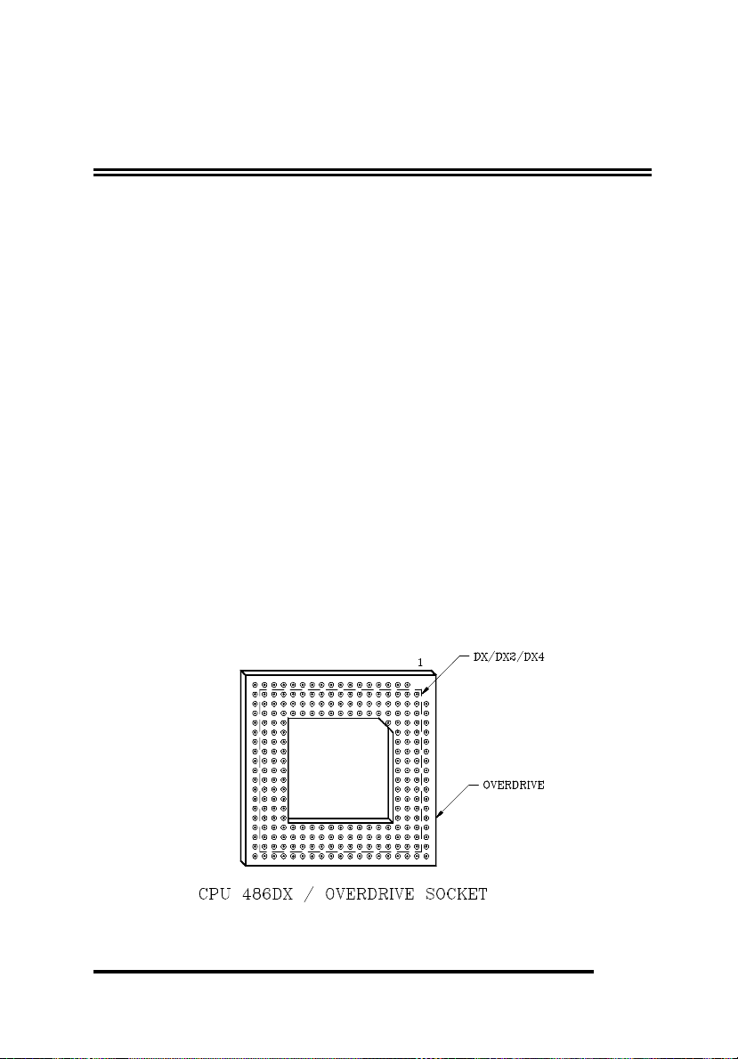
INSTALLING PROCESSOR (DX, SX, DX2, DX4)
Processor 486DX/DX2/DX4/P24T overdrive is a PGA devices.
There isa 238-pin PGAsocketorZIPsocket. To installprocessor,
be sure to line up pin 1 of the CPU with pin 1 of the socket as
shown below. Makesure that the processor is firmly inserted into
thesocket.

Chapter TWO
2-2
For DX, SX, DX2 are 5V supply voltage. Due to the DX4 is
3.45V supply voltage,a sohisticated on board auto detect voltage
regulatoris implemented on OCTEK HIPPO DCA 1. Therefore,
it’s no need to add any jumpers for different CPU.
INSTALLING RAM MODULES
OCTEK HIPPO DCA 1 has four sockets on board for 72pin
SIMM modules. The modules should be locked by the sockets.
Please check carefully before turning on the power. Otherwise,
the system will not work properly.
To install a module, the module edge is angled into the socket's
contact and then the module is pivoted into position, where the
locking latcheswill secure it. If themoduleedgeis notcompletely
inserted into the socket, it cannot be pivoted to be in vertical
position and should be dragged out and re-inserted again. Do not
forcethemoduleinto theSIMMsocket. It will damagethelocking
latches.
Chapter TWO
2-3
CONFIGURATIONOF MEMORY
There are severalcombinations ofDRAMtypesyoumay consider.
1Mx32 or 4Mx32 SIMM are acceptable. The memory size is
detected automatically by system BIOS and indicated during
memory test after reset. No jumper is needed to be set for the
memory size and DRAMtype.
DRAMCONFIGURATION
SM1
SM2
SM3
SM4
TOTAL
1Mx32
4M
1Mx32
1Mx32
8M
1Mx32
1Mx32
1Mx32
12M
1Mx32
1Mx32
1Mx32
1Mx32
16M
4Mx32
16M
1Mx32
4Mx32
20M
1Mx32
1Mx32
4Mx32
24M
1Mx32
1Mx32
1Mx32
4Mx32
28M
4Mx32
4Mx32
32M
1Mx32
4Mx32
4Mx32
36M
1Mx32
1Mx32
4Mx32
4Mx32
40M
4Mx32
4Mx32
4Mx32
48M
1Mx32
4Mx32
4Mx32
4Mx32
52M
4Mx32
4Mx32
4Mx32
4Mx32
64M

Chapter TWO
2-4
CONTROL OF SYSTEM SPEED
Systemspeed can be controlled by keyboard and turboswitch. To
change the speed by keyboard, use `-' and `+' of the numeric
keypad. Press `Ctrl' `Alt' and `-' for slow speed and press `Ctrl'
`Alt' and `+' forfast speed.
ConnectP1to theturboswitch of thecase and P5 to theturboLED
of the case. When the turbo mode is selected, the turbo LED of
thecase will be turned on.
Whenever the system speed is set to be slow by turbo switch, it
cannot be changed by the keyboard, and viceversa.
RESETCMOS SETUP INFORMATION
Sometimes, the improper setting of system setup may make the
system malfunction. In this case, turn off thepowerand set JP10
to 2-3 for a while. The internal CMOS status register is reset.
Then set the jumper to 1-2 of JP10 and turn on the power. The
BIOS finds the CMOS statusregisteris reset and regards the setup
information is invalid. So it will prompt you to correct the
information.

Chapter TWO
2-5
SYSTEMBOARD JUMPERSETTING
There are several options which allows user to select by hardware switches.
Display Selection
JP7
1-2
CGA, EGA, VGA
2-3
Monochromedisplay*
CPU Type
486DX\DX2
\DX4
486SX
487SX
JP6
1 - 2
2 - 3
1 - 2
JP8
2 - 3
NO
1 - 2
JP9
2 - 3
1 - 2
2 - 3
System Speed (Only for clock chip version)
33MHz
25MHz
JP4
1 - 2
2 - 3
JP5
1 - 2
2 - 3
Chapter TWO
2-6
CPU Clock Multiple (Only for DX4 CPU)
JP17
1-2
InternalClock3X
3-4
InternalClock2X
5-6
InternalCLock2.5X
SYSTEMBOARD CONNECTORS
Under typicalconditions, theseconnectors should be connected to
the indicators and switches of the system unit. The functionsof
connectorson the motherboard arelisted below.
Description
P1
Turboswitch
P2
Speakerconnector
P3
Hardwareresetconnector
P4
PowerLED& Ext-lockconnector
P5
TurboLED
P6,P7
Powersupplyconnector
P8
Externalbatteryconnector
P9
Coolingfanconnector
KB1
Keyboard connector
Pin assignment of the connectorare illustrated as follows:
P1 - Turbo Switch Connector
Pin
Assignment
1
SelectionPin
2
Ground
Chapter TWO
2-7
P2 - Speaker Connector
Pin
Assignment
1
Dataout
2
+5 Vdc
3
Ground
4
+5 Vdc
P3 - Hardware Reset Connector
Pin
Assignment
1
SelectionPin
2
Ground
P4 - Power LED & Ext-LockConnector
Pin
Assignment
1
+5 Vdc
2
Key
3
Ground
4
Keyboardinhibit
5
Ground
P5 - Turbo LED Connector
Pin
Assignment
1
+5Vdc
2
LED signal

Chapter TWO
2-8
P6,P7 - Power Supply Connector
Pin
Assignment
1
POWERGOOD
2
+5 Vdc
3
+12 Vdc
4
-12 Vdc
5
Ground
6
Ground
Pin
Assignment
1
Ground
2
Ground
3
-5 Vdc
4
+5 Vdc
5
+5 Vdc
6
+5 Vdc
P8 - External Battery Connector
Pin
Assignment
1
+ Vdc
2
not used
3
Ground
4
Ground
P9 - Cooling Fan Connector
Pin
Assignment
1
+ 5Vdc
2
Ground

Chapter TWO
2-9
KB1 - Keyboard Connector
Pin
Assignment
1
Keyboardclock
2
Keyboarddata
3
Spare
4
Ground
5
+5 Vdc

Chapter TWO
2-10
THIS PAGE IS INTENTIONALLY LEFT BLANK

Chapter THREE
3-1
Chapter Three
Technical Information
This section providestechnicalinformationaboutOCTEK HIPPO
DCA 1 and is intended for advancedusers interested in the basic
design and operation of OCTEK HIPPO DCA 1.
MEMORY MAPPING
Address
Range
Function
000000-
7FFFFF
000K-512K
System BoardMemory
(512K)
080000-
09FFFF
512K-640K
System BoardMemory
(128K)
0A0000-
0BFFFF
640K-768K
DisplayBuffer(128K)
0C0000-
0DFFFF
768K-896K
AdaptorROM / ShadowRAM
(128K)
0E0000-
0EFFFF
896K-960K
System ROM / Shadow
RAM (64K)
0F0000-
0FFFFF
960K-1024K
System BIOS ROM / Shadow
RAM (64K)
100000-
7FFFFF
1024K-
8192K
System Memory
800000-
FFFFFF
8192K-
16318K
System Memory

Chapter THREE
3-2
I/O ADDRESS MAP
I/O AddressMap on System Board
I/O address hex 000to 0FF are reserved for the system board I/O.
ADDRESS
(HEX)
DEVICE
000-01F
DMAController1,8237
020-03F
InterruptController1,8259,Master
040-05F
Timer,8254
060-06F
Keyboard Controller
070-07F
Real Time Clock,NMI
(non-maskableinterrupt)mask
080-09F
DMAPage Register,74LS612
0A0-0BF
InterruptController2,8259
0C0-0DF
DMAController2,8237
0F0
ClearMathCoprocessorBusy
0F1
Reset MathCoprocessor
0F8-0FF
Math CoprocessorPort
Table of contents


