manuals.online logo
Brands
  1. Home
  2. •
  3. Brands
  4. •
  5. Hitachi
  6. •
  7. HDTV
  8. •
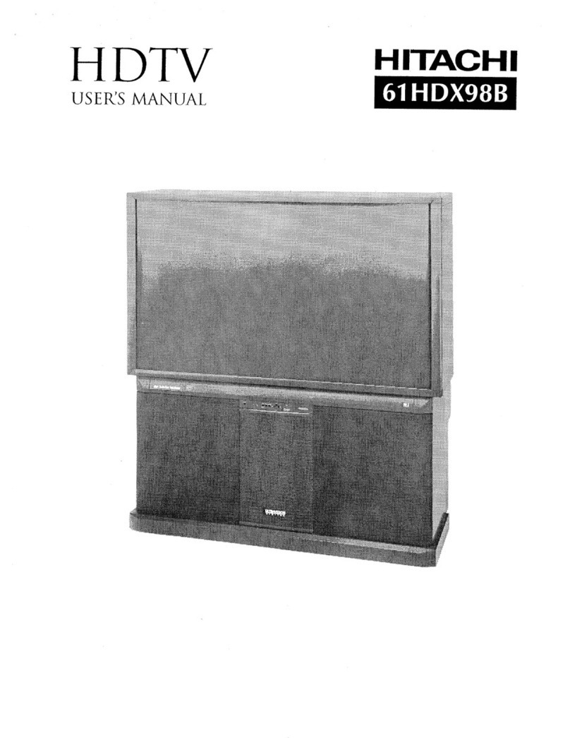
  9. Hitachi 61HDX98B User manual

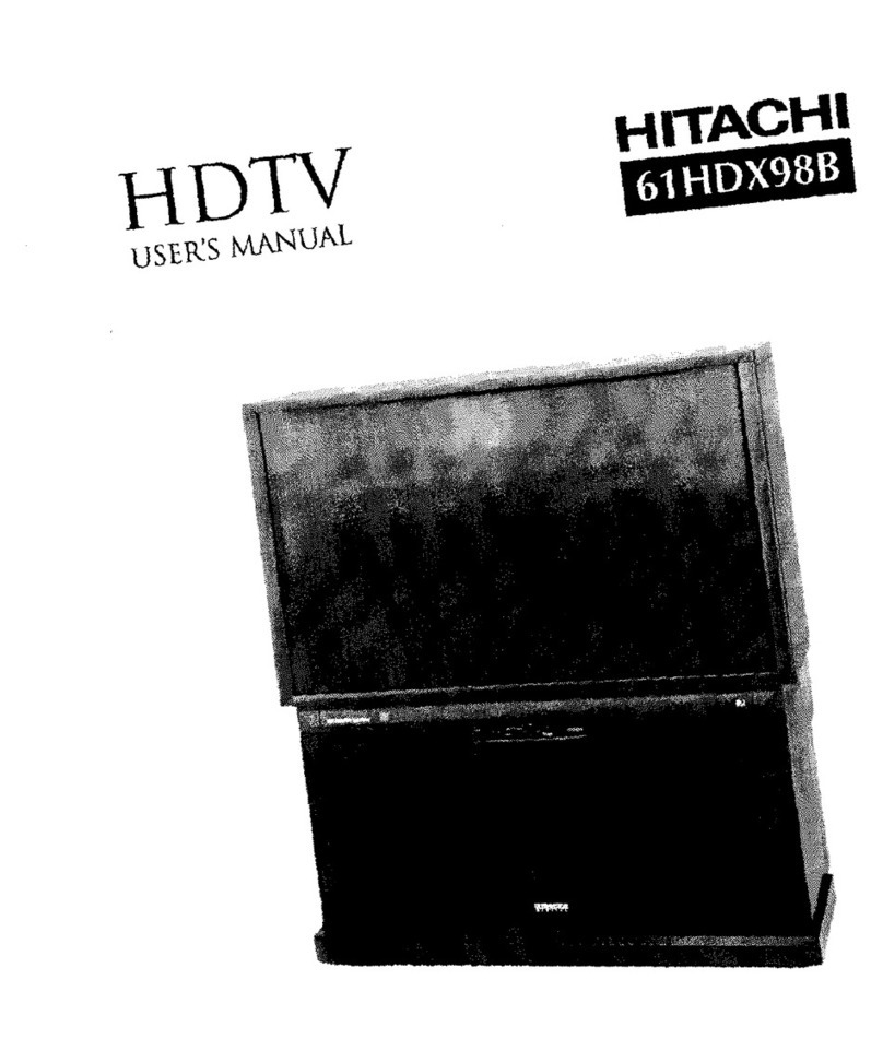
Hitachi 61HDX98B User manual

CONTENTS... 1999 DP-85 HDTVProjectionTelevisionInformation
NOVEMBER,1999 Prepared by: ALVIERODGERSC.E.T.
This training package is geared specifically to the 61HDX98B HDTV. However, most of
the material will cross over to the 60SDX88B progressive scan HDTV capable set. The
necessary understanding that the 60SDX88B requires a Set-Top-Box to receive SDTV and
HDTV signals is important. The 60SDX88B does NOT have a DM-1 module. This module
is built into the 61HDX98B which allows this set to receive all ATSC formats as well as
Direct TV, NTSC, SDTV or HDTV. It does not have Component Inputs.
The 60SDX88B has a built in FLEX converter that translates any input into either 480P for
NTSC or SDTV and/or 1080I for HDTV. It does have Component Inputs.
The Power Supplies are the same for either set.
The Deflection circuit is very similar between the two sets.
The Signal PWB is very similar between the two sets, minus the differences mentioned
above.
Digital Convergence is the same between the two sets.
61HDX98B is a DP-85 chassis with a 16X9 aspect screen.
60SDX88B is a DP-86 chassis with a 3X4 aspect screen.
SEE DP-86 TRAINING SECTION IN THE BACK OF THE PACKAGE.
CONTENTS
”SECTION” “PAGE”
DP-85 CHASSIS TRAINING and INFORMATION” HDTV
CONTENTS PAGE (A-1)
1): GENERAL BLOCK DIAGRAMS, SECTION:
•Power Supply Block Explanation --------------------------------------------------------- 01-01
•Power Supply Block Diagram ------------------------------------------------------------- 01-02
•DM-1 Module Front End Block Explanation -------------------------------------------- 01-03
•DM-1 Module Front End Block Diagram ------------------------------------------------ 01-05
•AV Selector Block Explanation ------------------------------------------------------------ 01-06
•AV SelectorBlock Diagram ---------------------------------------------------------------- 01-07
•System Control Block Explanation ------------------------------------------------------- 01-08
•System Control Block Diagram ----------------------------------------------------------- 01-10
•2H Video Block Explanation --------------------------------------------------------------- 01-11
•2H Video Block Diagram ------------------------------------------------------------------- 01-12
•Deflection Circuit Block Explanation ---------------------------------------------------- 01-13
•Deflection Circuit Block Diagram -------------------------------------------------------- 01-16
•CRT Block Diagram ------------------------------------------------------------------------- 01-17
•Audio Output Block Diagram ------------------------------------------------------------- 01-18
•Rear Panel Diagram ------------------------------------------------------------------------- 01-19
•4X3 Displayed on 16X9 Four Possible Modes ------------------------------------------- 01-20
2): POWER SUPPLY INFORMATION, SECTION:
•Digital Circuit Power Supply SHUT DOWN Block Diagram -------------------------- 02-01
•Digital Circuit Power Supply SHUT DOWN Circuit Diagram ------------------------- 02-02
•Digital Circuit Power Supply Visual Trouble Shooting LED's Diagram ------------- 02-03
•Digital Circuit Power Supply Distribution Diagram-------------------------------------- 02-04
•Deflection and High Voltage Power Supply SHUT DOWN Block Diagram --------- 02-05
•Deflection and High Voltage Power Supply SHUT DOWN Circuit Diagram -------- 02-06
•Deflection Power Supply Visual Trouble Shooting LED's Diagram ------------------ 02-07
•Deflection Power Supply Distribution Diagram ------------------------------------------ 02-08
3): HORIZONTAL DRIVE, SECTION:
•Horizontal Drive Circuit Diagram --------------------------------------------------------- 03-01
4): VIDEO SIGNAL INFORMATION:
•Video Signal Main and Terminal Circuit Diagram -------------------------------------- 04-01
•ABL Circuit Diagram ------------------------------------------------------------------------- 04-02
•Horizontal and Vertical SWEEP LOSS DETECTION Circuit ------------------------ 04-03
5): AUDIO CIRCUIT INFORMATION:
•Audio Signal Main and Terminal Board Circuit Diagram ----------------------------- 05-01
•Audio SURROUND Board Circuit Diagram ---------------------------------------------- 05-02
•Audio and Video MUTE Circuit Diagram ------------------------------------------------ 05-03
•Audio MUTE Surround Board Circuit Diagram ----------------------------------------- 05-04
•Audio MUTE Audio Output Board Circuit Diagram ------------------------------------ 05-05
6): DIGITAL CONVERGENCE CIRCUIT INFORMATION:
•Digital Convergence INTER-CONNECTION Diagram -------------------------------- 06-01
CONTENTS
”SECTION” “PAGE”
DP-85 CHASSIS TRAINING and INFORMATION” HDTV
CONTENTS PAGE (A-2)
•Digital Convergence OVERLAY Information -------------------------------------------- 06-02
•Digital Convergence OVERLAY DIMENSIONS --------------------------------------- 06-03
•Digital Convergence REMOTE CONTROL Button Identification ------------------- 06-04
7): MICROPROCESSOR
•Microprocessor Port Definitions ......................................................................................07-01
•Microprocessor Data Port Block Diagram .......................................................................07-03
•Microprocessor Data Communications Block Diagram ...................................................07-04
8): ADJUSTMENTS
•Adjustment Order ...............................................................................................................08-01
•I2C Bus Alignments in the Field...........................................................................................08-02
•Centering Magnets Location...............................................................................................08-06
•Pre Heat Run Condition.......................................................................................................08-07
•Cut Off and Focus Adjustment ............................................................................................08-08
•Digital Convergence Unit Crosshatch Phase......................................................................08-09
•Horizontal Position “Coarse” Adjustment..........................................................................08-10
•Raster Tilt (Deflection Yoke) Adjustment..........................................................................08-11
•Beam Alignment Adjustment..............................................................................................08-12
•Centering Magnet and Beam Shape Magnet Identifications............................................08-13
•Static Centering and Center Adjustment ........................................................................08-14
•Horizontal Blanking Phase Adjustment..............................................................................08-15
•Horizontal & Vertical Size Adjustment................................................................................08-16
•Trapezoid Distortion Adjustment .......................................................................................08-17
•Side Pincushion Distortion Adjustment ..............................................................................08-18
•Beam Form Adjustment ......................................................................................................08-19
•Optical System Alignment (Lens)........................................................................................08-20
•Blue Defocus Adjustment ....................................................................................................08-21
•Red, Green and Blue White Balance Tracking.....................................................................08-22
•Sub Brightness Adjustment Alternate Method .....................................................................08-23
•Horizontal Position “Fine” Adjustment ...............................................................................08-24
DIGITAL CONVERGENCE ALIGNMENT PROCEDURE
•Digital Convergence Overlay Smooth and Full.................................................................08-25
•(3X3) and (7X5) Stopping positions.....................................................................................08-26
•(13X9) Stopping positions....................................................................................................08-27
•Digital Convergence Remote Control.................................................................................08-28
•Clearing RAM Data .............................................................................................................08-29
•Raster Centering .................................................................................................................08-30
FULL MODE
•Green 3X3 Adjustment ......................................................................................................................08-31
•Red and Blue 3X3 Adjustment ..........................................................................................................08-32
•Green 7X5 Adjustment ......................................................................................................................08-33
CONTENTS
”SECTION” “PAGE”
DP-85 CHASSIS TRAINING and INFORMATION” HDTV
CONTENTS PAGE (A-3)
•Red and Blue 7X5 Adjustment ..........................................................................................................08-34
•Green 13X9 Adjustment ....................................................................................................................08-35
•Red and Blue 13X9 Adjustment ........................................................................................................08-36
•Storing New Dig. Conv. Data ...........................................................................................................08-37
•Magic Focus Initialization ................................................................................................................08-38
SMOOTH MODE
Change Screen Format to SMOOTH Mode and repeat steps below.
•Green 7X5 Adjustment (If necessary) ...............................................................................................08-33
•Red and Blue 7X5 Adjustment (If necessary) ...................................................................................08-34
•Green 13X9 Adjustment ....................................................................................................................08-35
•Red and Blue 13X9 Adjustment ........................................................................................................08-36
•Storing New Dig. Conv. Data ...........................................................................................................08-37
•Magic Focus Initialization ................................................................................................................08-38
•Static Centering Adjustment .......................................................................................................... 08-39
Minor Digital Convergence Adjustment
•Minor Adjustments Needed ............................................................................................................08-40
•Accessing Digital Convergence Error Codes ..................................................................................08-41
Adjustments Continued
•Memory Initialization Procedure .......................................................................................................08-42
9): TROUBLE SHOOTING
•No Raster No Power ..........................................................................................................................09-01
•A and B: No Relay Click, Def. Red LED Blinking ...................................................................09-02
•C and R: No Red LED B+ .........................................................................................................09-03
•D, E and F: All LED’s going off at the same time Def. and Power PWB ................................09-04
•G One LED going off a little before the others Dig. and Sig. Power PWB ..............................09-05
•DM-1Trouble Shooting Figure .......................................................................................................09-06
•DM-1 Troubleshooting Checks ........................................................................................................09-07
•DM-1 Waveforms used for Troubleshooting ..................................................................................09-08
•DM-1 Video Waveforms Troubleshooting Checks ........................................................................09-08
•Deflection Waveforms Troubleshooting Checks ............................................................................09-10
•Other Key Waveforms Troubleshooting Checks ............................................................................09-13
•Smart Card Troubleshooting Checks .............................................................................................09-18
10): COMPONENT IDENTIFICATION AND PARTS INFORMATION
•Component and Parts Identification ...............................................................................................10-01
ADJUSTMENTS CONTINUED
Page 01-01
The 61HDX98B utilizes two switching power sup-
plies.
DP-85's stand by switching mode operation is different
from AP-7X and 8X chassis's. Switching frequency of
AP-7X and 8X chassis is dropped to 20kHz during
stand by mode. But the DP-85's power supply is not
dropped during stand by mode. DP-85's is operated
about 100kHz.
Normally Power Supply switching is operated as fol-
lowing.
T901: 25-56 kHz (Normal)
100-200 kHz (Stand by)
TP91 30-53 kHz (normal)
POWER SUPPLY UTILIZED FOR THE DIGI-
TAL AND SIGNAL CIRCUITS:
(Sub Power Supply PWB)
This supplies power primarily to the Digital circuits, i.
e. DM-1 module. This supply runs anytime the set is
plugged into an AC outlet.
The voltages produced are;
•+33V,
•Power for the Satellite dish which is switched be-
tween 13V and 19V dependant upon the channel
being received.
•Stand By 12V also called A12V
•TV9V
•TV5V
•3.3V
•-5V
POWER SUPPLY UTILIZED FOR THE DE-
FLECTION, AUDIO and DIGITAL CONVER-
GENCE CIRCUITS: (Deflection PWB)
This supply only operates when the set is turned ON.
When the ON command is received from the DM-1
module, relay S-901 energizes and delivers AC to the
main bridge rectifier D903 located on the Sub Power
Supply PWB.
This supplies power primarily to the Deflection circuit
for the collector of the High Voltage generation circuit
and the collector of the Deflection Output transistor.
Also, the Convergence output amps and the Audio
output amps derive their voltages from here as well.
The voltages produced are;
•+130V used for Deflection and High Voltage cir-
cuits.
•220V used for the collectors of the R, G, B drivers
on the CRT PWB and the Velocity Modulation
circuits.
•6.3V to drive the CRT Heaters.
•+28V for the Convergence, Velocity modulation
and Audio Out circuit.
•+13V for Vertical.
•-13V for Vertical and also converted down to
the –5V for the Digital Convergence Unit.
The TV9V supply generated from the Power Supply
for Digital listed above, is regulated down to +5V for
the Digital Convergence Unit and the A12V for the
Power Supply for Digital is used as a switched On/Off
for the Deflection Vcc by the Rainforest IC.
BLOCK DIAGRAM EXPLANATION POWER SUPPLY BLOCK
IP01
Main
Switching
Regulator
EE49
Relay
Line
Filter
R
I901
Sub
Switching
Regulator
EE42
Line
Filter
STAND BY
C21V
R/F 28V
-7V
24.5V
SWITCHED
Def. +B V1&V2
35V
CRT &
Vm Out
Convergence
Velocity Mod.
Audio Out
Convergence
Vertical
Vertical (M13)
DCU
Heater
To Signal Block
POWER SUB P.W.B.
DP85 POWER SUPPLY BLOCK
DIAGRAM
Fuse
(130V) Reg
220V
+28V
-28V
+13V Reg.
-13V Sw. Reg.
-5V Reg.
6.3V
AC108-
132V/
60Hz.
AC Inlet Type
To Deflection Block
Page 01-02
POWER DEFLECTION P.W.B.
+33VS Reg
-5V Sw. Reg.
28V
21V
Power Fail
L. NB Sw. Reg.
A12V Sw. Reg.
9V Sw. Reg. TV9V
5V Sw. Reg. TV5V
3.3V Sw. Reg.
3.3V Sw. Reg.
HVcc12VA12V
+5V Reg.TV9V DCU
Page 01-03
The 61HDX98B utilizes a non-repairable Front End
Assembly called the DM-1 Module. This module con-
tains the main System control center, NTSC Front
End, Direct TV Receiver and ATSC Tuner. The block
diagram indicates the internal blocks contained within
the Front End Assembly, hear after called the DM-1.
Starting counterclockwise from the upper left.
SATELLITE:
This represents the Direct TV satellite dish connection
to the back of the set.
SATELLITE TUNER/IF:
This is the internal IRD, (Integrated Receiver and De-
coder). This receives the satellite signal from the LNB
(Low Noise Block) located on the Dish. This block
converts the signal to a usable signal for decoding.
SATELLITE CARD and SATELLITE LINK
BLOCK:
To receive Direct TV signals, the customer is required
to insert an active Security Card into the back of the
set. This care contains a programmable chip that con-
tains the consumer’s information and the channels that
the consumer is allowed to receive. Also, this card is
used when billing information is retrieved by Direct
TV.
LINK/MIX:
This block passes the particular signal that the cus-
tomer has decided to view on screen. Either the Direct
TV signal or the ATSC tuner.
TERRESTRIAL:
This indicates the outside antenna the consumer has
erected to receive NTSC signals as well as ATSC sig-
nals.
CABLE:
This is the input from the consumer’s cable signal.
HD/NTSC TUNER/IF SPLITTER:
This block receives the Terrestrial signal and depend-
ant upon which source the consumer has decided to
view, processes the signal through the appropriate
tuner.
•HD: Receives the Terrestrial Signal and routes it
to the ATSC tuner. This tuner is capable of re-
ceiving all 18 ATSC formats.
•NTSC: Receives the Terrestrial Signal and route
it to the NTSC Tuner.
•The NTSC signal is routed out of this block on the
line labeled Composite Video to the Signal Selec-
tor IC which selects the appropriate signal accord-
ing to the consumer’s choice. Either Tuner,
AVX1, 2 or 3 and/or S-In 1,2 or 3.
•The NTSC audio IF signal is routed to the MTS
STEREO DECODER.
•SPLITTER:
•The splitter routes the NTSC signal out to the RF
Out PinP Tuner path to the PinP Tuner.
MTS STEREO DECODER:
Decodes the NTSC Audio IF signal an decodes it into
Left Total and Right Total. This signal is routed to the
Dolby®Pro-Logic decoder.
HDTV LINK:
This block routs the ATSC signal received by the
ATSC tuner to the Link Mix.
NTSC YUV A/D:
This block receives the NTSC luminance and chroma
signals and converters them to a digital signal to be
utilized by the MPEG VIDEO decoder.
FROM MAIN MICRO:
This is communication in and out for the Sub-
Microprocessor. Information such as the Selector IC
selection, power on/off commands, etc.., are routed
from the ARM/Transport or Main Microprocessor sec-
tion.
SD-A/V:
This is the output of the AC-3 digital audio to be used
by an off board AC-3 decoder.
MODEM:
Direct TV polls the Direct TV receiver section through
the customer’s phone lines and determines such things
as Pay for View authorization, customer’s informa-
tion, Card authorization and billing information.
ARM/TRANSPORT:
The Arm/Transport block receives all signals from Di-
rect TV, ATSC. It also receives the Infrared remote con-
trol signals, Front panel Key data, and Slave Microproc-
essor information. This is the Main Microprocessor sec-
tion of the DM-1 module. Dynamic RAM and ROM in-
formation is processed from Soft ward load into ROM
and determines the state of the Television. Information
from ATSC and/or Direct TV is routed to the MPEG
VIDEO DECODER.
BLOCK DIAGRAM EXPLANATION FRONT END
Page 01-04
MPEG VIDEO DECODER, NTSC UPCONVER-
SION, OSD:
What ever signal is requested by the consumer as the
source for viewing is processed through this block and is
output to the YUV D/As.
YUV/DAs:
This block takes the digital signals provided to it and
converts them to an analog signal which is usable by the
signal processing circuits.
All signals are routed out through the line labeled 2.14
YUV/YIQ, (NTSC Signal up converted to 480P or 2.14
HYPBPR which is the HDTV output as 1080I.
MPEG/AC-3 AUDIO DECODER:
This block processes the audio component from the
ARM/TRANSPORT or the block A/Ds AUDIO, which
is the NTSC audio processed by the Pro Logic decoding
circuit, labeled as 5.1, (Front Left, Front Right, Center,
Rear Left and Rear Right + Sub Woofer audio also called
LFE. Then this block processes the signal and outputs all
audio to the Audio D/As.
AUDIO D/As:
This block is the Digital to Analog converter which con-
verts the digital audio signal sent to it by the ARM/
TRANSPORT block and converts it to a usable analog
signal to be processed by the audio output section.
The audio labeling is comprised of the following:
L/R = Audio Front Left and Right
LS/RS = Rear or Surround audio Left and Right
C/LFE = C for Center and LFE for Sub Woofer, also
called Low Frequency Effects.
BLOCK DIAGRAM EXPLANATION FRONT END
SATELLITE
TUNER/IF SATELLITE
LINK LINK
MIX
HDTV
LINK
HD/NTSC
TUNER/IF
SPLITTER
MTS
STEREO
DECODER
NTSC YUV
A/D
ARM/
TRANSPORT DRAM
ROM
NRSS/ISO7815
MPEG/AC-3
AUDIO
DECODER
MPEG VIDEO
DECODER
NTSC
UPCONVERSION
OSD
YUV
D/As
SRAM A/D's
AUDIO EEROM
AUDIO
D/A's
SD-A/V MODEM
PhoneSD-
Satellite
Card
DM-1 Module
Satellite
RF Out
PinP
Tuner
Cable
Terrestrial
L/R Composite
Video 1HYIQ From
Main
Micro L/R
LS/RS
C/LFE
L/R
Data
Address
Handshake
5.1 Audio
DP85 FRONT END
BLOCK
From Main Micro
2.14YUV/YIQ
2.14 HYPBPR
Page 01-05
VSB
IR from Ft. Panel
Dimmer, AD, Key In
To 2H Video Circuit
Digital
Page 01-06
C. VIDEO (MAIN) and R/L (AUDIO MAIN):
NTSC Video and NTSC Audio is routed from the
DM-1 Block diagram. They are shown in the Block
Diagram as one line, but they are separate signals.
Anytime a signal is routed from the DM-1 or going to
the DM-1 module, they must be sent through a DM-1
I/F block. This block reduces the noise by a noise can-
cellation process. This process uses the output of a
comparator and routes the output back to the negative
input to subtract the noise. It also level shifts the signal
to make it useable by the circuit to which it is routed.
DM-1 I/F BA4558:
This is the noise cancellation and level shift block.
AUDIO/VIDEO SELECTOR TA8851BN:
This is the selector IC. Dependant upon the customer’s
viewing preference, the DM-1 will communicate via
I2C bus communications and select the NTSC signal
which is sent to the demodulator. The demodulator
prepares the NTSC signal for the DM-1 module.
This IC selects the following inputs;
Main tuner
Video One, Two or Three
S-In One, Two or Three
PinP Video and Audio outputs. This can be any of the
input provided above except the PinP has it’s own
tuner.
Note: PinP isn’t available when the customer has se-
lected Direct TV or ATSC as it’s source. This is be-
cause, as will be shown later, the PinP Video is super
exposed upon the NTSC video only.
Any video source selected for the Main picture will be
routed to the 3D Y/C module.
Note: There are NO Component inputs on this set.
BLOCK DIAGRAM EXPLANATION A/V SELECTOR
A/V SELECTOR BLOCK DP85
CHASSIS
TERMINAL P.W.B.
Page 01-07
Comp. Video (Main) R/L (Main)
PinP Video and
MonoAudio
PinP L/R Out
To Audio Out PWB
C. Video (Main)
R/L (Audio Main)
Selected L/R
(NTSC Main Audio)
Video 4 V4, S4, L/R4 PinP Video
to PinP Unit
Video D YC
To 3DYC
9V
V1 S1 L/R1
V2 S2 L/R2
V3 S3 L/R3
Video One In
Video Two In
Video Three In
DM-1
I/F
B4558
I2C
AUDIO/VIDEO
SELECTOR
TA8851BN
PinP
Tuner U001
RF from DM-1
VT+33V Lock
Clock
Data
Enable
+5V +9V
PinP
Video
Mono
Page 01-08
MAIN VIDEO FROM SELECTOR IC:
At the bottom left hand side is shown the Main Video
from Selector label. This is the NTSC video from the
selector IC. This is routed to two blocks.
3D Y/C:
The 3D Y/C separates luminance from the chroma. It
also add the 3D effect, (if the 3D Y/C is turned on
within the menu). Noise is canceled and the two sepa-
rate components are output to the Video/Chroma De-
modulator.
VIDEO/CHROMA DEMODULATOR:
This IC decodes the signal down to it’s Luminance and
Chroma. components and outputs it as 1HYIQ.
DM-1 I/F:
Noise cancellation and level shifting preparing the sig-
nal for the DM-1 module.
1HYIQ:
1HY = Standard NTSC format luminance. (Also
known as 480I).
I and Q = Standard NTSC format, demodulated
chroma components.
SYNC DET.:
Separates the Sync signal from the composite video sig-
nal.
SYNC DET.:
This block outputs composite sync to the PinP unit which
is used for timing for display. This is specifically related
to the Demodulator, D/As and Read/Write clock. The
Read/Write clock also is controlled by the frequency of
the Subcarrier also called fsc.
The Composite sync is also sent to the DM-1 on the line
labeled as 1H Composite Sync. The DM-1 uses this sig-
nal for OSD positioning, auto channel detection and AFC
loop activation.
TV uCOM MICROPROCESSOR:
This is the slave Microprocessor or Sub-Microprocessor.
This IC is in constant communications with the DM-1
module. The slave uP. Receives or outputs the following
signals;
HBLK: = Input; this is the Horizontal Blanking signal.
Used for Service OSD signal creation timing.
S.WIDE: = Output; when the customer watches regular
NTSC 4X3 aspect source, they have a choice of viewing
the signal in one of 4 ways.
Normal: This will display a standard 4X3 picture
with black panels on each side of the picture.
Fill: This will expand the picture to fill the screen.
The top and bottom will be cropped.
Full: This will expand the picture side ways and fill
the screen. However the picture will be non-linear.
Smooth Wide: This will keep the center of the pic-
ture linear and stretch the outside edges to fill the
screen.
With the four choices above, the DM-1 module controls
the signal for 3 of them; Normal, Fill and Full. However,
during Smooth Wide, the deflection circuit is switched to
perform the stretching of the sides. The slave Microproc-
essor outputs S.Wide during this time.
CUT OFF: = Output; labeled as V. Stop, during the Ser-
vice adjustments for Cut Off, (Screen Background con-
trols), the vertical must be collapsed. This output causes
the B+ to the vertical output IC front end to be grounded
and grounds the vertical trigger pulse called V. Saw.
D. SIZE: = Output; labeled as Digicon Size, during
Smooth Wide mode, the Digital Convergence Unit, hear
after called DCU, must know that the set is in the dis-
torted deflection mode. This signal tells the DCU just
that.
MAGIC SW: = Input; when the customer presses the
Magic Focus button on the control panel, the DCU noti-
fies the slave micro. That it is busy performing Magic
Focus. The slave micro. Notifies the DM-1 module and
the DM-1 module ignores infrared pulses from the re-
mote control.
CLOSED CAP. DATA: = Input; This input receives the
composite sync signal and decodes the Closed Caption
Data. (Data Slice line 21) and the communicates with the
DM-1 Module. The DM-1 Module actually introduces
the Closed Caption Characters into the Video stream.
F. PANEL: = Output, Dependant upon the customer’s
menu selection, will determine the IRE level of the side
panels when 4X3 Normal mode is used. By raising the
side panel IRE levels, the 4X3 picture won’t burn in the
CRT’s.
MAIN SYNC DET: = Input; this is used for detecting the
Closed Caption Data. This information is routed to the
DM-1 module for OSD generation. NOTE: the sub-
micro. Doesn’t produce OSD characters for Closed Cap-
tion.
PinP SYNC DET: = Input; PinP tuner sync is routed to
the sub-micro. And is used during PinP tuner channel
BLOCK DIAGRAM EXPLANATION
SYSTEM CONTROL AND SIGNAL PROCESSING
Page 01-09
selection to activate AFC.
MAIN SYNC DET. = Input; This input is used for Ser-
vice OSD positioning and Auto Programming channel
detection.
PinP SYNC DET. = Input; This input is used for judge-
ment of the Slave Microprocessor to determine the AFC
Loop activity of the PinP Tuner.
MUTE (Audio): = Output; during channel change, ex-
ternal video selection with no input, power up or power
off, and loss of Vertical Blanking, the audio and video
are muted.
V.MUTE (Video): = Output; during child lock, channel
change, or power on/off, the video is muted.
POWER: = Output; when the front power button or the
remote power button is pressed, the DM-1 module noti-
fies the sub-micro. And the sub-micro. Outputs a power
on/off command to the relay driver Q-007. Outputs high
for ON and low for OFF.
OSD & OSD BLK: = Output, this is the on screen char-
acters for the Service Menu only. OSD Blk is OSD
blanking. This cleans us the video where the OSD is to
be inserted.
HV BLK: = Input; this inputs are utilized by the Micro-
processor for Service OSD positioning.
HV BLK PH: = Output; during Service Adjustment and
in the NTSC normal mode. This picture doesn’t fill the
screen. The areas on the side of the picture are called
Side Panels. This can be adjusted. The HV BLK PH,
controls the timing of the side panel OSD outputs.
SIDE PANEL APL FROM 2H VIDEO PWB: = Input;
the Microprocessor receives a pulse created within the
2H video PWB. This pulse represents the timing pulse
for the Side Panel OSD production.
Blocks continued;
OSD MIX: Only the Service menu OSD is output from
the Slave Microprocessor. The Digital convergence unit
puts out OSD characters as well. This characters product
the Service Grid and other text during Digital Conver-
gence adjustments and/or Magic Focus. The two OSD
sources are received by the OSD Mix. This is comprised
of a quad Or Gate and outputs the signal to be superim-
posed upon the video signal path from the DM-1 Mod-
ule.
PinP VIDEO FROM SELECTOR IC: The video from
the PinP tuner is routed to the PinP unit and the Sub Mi-
croprocessor for Closed Caption decoding.
BLOCK DIAGRAM EXPLANATION
SYSTEM CONTROL AND SIGNAL PROCESSING
TV uCOM
Microprocessor
DP-85 CHASSIS SYSTEM CONTROL & SIGNAL PROCESSING
BLOCK
SIGNAL P.W.B.
Page 01-10
H Sync
PinP
Sync Det.
PinP V
F Panel
Main Sync Det
PinP Sync Det
Mute (Audio)
V.Mute (Video)
Power
OSD & OSD Blk
for Service Menu
HBlk
S. Wide
Cut. Off
D. Size
Magic Sw.
Closed Cap. Data
MEMORY I2C
I2C
VIDEO/
CHROMA
DEMOD
3D
Y/C
Unit
PinP
Unit
Sync Det.
Sync Det.
DM-1
I/F
OSD
MIX
+
Digital OSD / Busy
OSD RGB Ys
OSD
RGB Ys
V Sync
I2C
Y/C
Y
PinP
Video
Y/C
PinP Video from Selector
IC
1 H Composite
Sync
1HYIQ
Main Video from Selector IC
YIQ
YIQ Mix Clamp
AD8056
CCD Video
Main
CCD Video
PinP
H BLK PH
HV BLK
Side Panel
APL
from 2H
Video PWB
Page 01-11
The 2H Video PWB is similar to the Rainfor-
est circuits used in the past. The YUV/YIQ
(480P) and/or the Y-PR/PB (1080I) is routed
through another DM-1 Interface IC for noise
cancellation and level shifting and into the
Rainforest chip, IX01. Here the signal is pre-
pared for the CRT’s. Pedestal level detection,
Chroma preparation, OSD RGB from either
the DCU or the Slave Microprocessor is input
here.
Remember that the OSD for Customer usage
such as the Channel numbers, clock, Main
Menu, etc.. is generated by the DM-1 Mod-
ule.
Also, ABL controls the brightness and
Contrast; as well as the color level at this
chip.
The Velocity modulation control signal is
produced from the Rainforest IC. This signal
is a representative of the Peak White compo-
nents of luminance and drives the Velocity
Modulation coils on each CRT.
BLOCK DIAGRAM EXPLANATION 2H VIDEO
YUV/YIQ/
Y PB PR
RGB PROCESSOR
TA1276AN
2 H VIDEO BLOCK DP-85
CHASSIS
2H VIDEO P.W.B.
Page 01-12
YUV RGB
+9V
RGB
APL
DETECT
HV. Blk.
Gen. HV Blk
HBLK PH
+9V
DM-1
I/F
CLAMP
GEN.
+5V -5V
2.14 HV SYNC
2.14 HV SYNC
SPANEL
Side Panel
APL
2.14 SYNC
+5V
Clamp H/V Blk.
VM
YUV
YIQ
YPBPR
Y
Clamp
YUV/YIQ/
Y PB PR
2.14 HV SYNC
OSD RGBABLI2C
Page 01-13
The 61HDX98B deflection circuit differs from con-
ventional Hitachi product. It utilizes in a sense, two
horizontal output circuits. One for Deflection and on
for High Voltage. The notations around the Block dia-
gram will be described in a counter clock wise fashion
as best a possible.
CUT OFF:
Cut of collapses the Vertical circuit during I2C Bus
alignments, during CRT Set Up.
I2C:
Communication from the Sub Microprocessor I001
during sweep variations due to Standard/NTSC 480P
mode and 1080I High Definition mode.
ABL:
ABL voltage is generated by monitoring the current
through the flyback transformer. This voltage will
fluctuate down when the scene is bright and up when
the scene is dark. The ABL voltage will manipulate
the screen brightness and contrast to prevent blooming
under these conditions.
HV SYNC:
The composite sync is routed into the Sync processor
which determines the sweep condition for the signal
being provided.
H and V BLK:
Horizontal and Vertical Blanking is developed within
the Deflection circuit. The Horizontal Blanking pulse
operates around 13V P/P and is produced by taking a
sample pulse from the Deflection transformer T752.
The Vertical Blanking pulse is generated from the
Vertical output IC, I601 pin 7. This pulse normally
operates at 23V P/P.
IR:
The Infrared Pulses coming from the remote control
are routed through the Deflection PWB to the Digital
Convergence Unit. During DCAM (Digital Conver-
gence Adjustment Mode), the Remote Control pro-
vides manipulation pulses for the DCU.
DIG RGB BUSY:
This indicates Digital RGB and BUSY.
Digital RGB represents the on screen characters pro-
duced by the DCU for generating the Digital Conver-
gence adjustment grid and text produced during cer-
tain conditions such as Magic Focus, Sensor Initializa-
tion, Data Storage, etc…
Busy notifies the sub Microprocessor I901 which in
turn notifies the DM-1 module that the DCU has en-
tered the DCAM. During this time, the DM-1 module
ignores the remote control commands.
MAGIC SW:
When the customer presses the Magic Focus button on
the front of the set, it produces a command for the
DCU to begin the Magic Focus process.
D SIZE:
Digital Size is a control signal for raster enlargement
when MAGIC FOCUS is operated. Raster enlarge-
ment is required for the MAGIC FOCUS PATTERN
to hit the photo sensors.
This signal is output from DCU and input to the Sub
Microprocessor I901. The Sub Microprocessor con-
trols the I702 on the DEF.SUB PWB) for enlarging
raster size.
In case of AP-85, this control signal is called "A.
SIZE". It's the same function between DIG.SIZE and
A.SIZE.
S WIDE:
Smooth Wide is a condition entered through the Menu
by the customer while watching an NTSC 4X3 aspect
video source and the customer wants to fill the screen.
TO CONVERGENCE YOKES:
The DCU provides compensation signal for deflection
abnormalities to the convergence output IC. The Con-
vergence output IC in turn, amplify the signals and
rout them to the convergence yokes.
+26V, 26VP and RETRACE PULSE:
The positive 26V and the negative 26V is routed to the
Deflection transformer I752. They enter the trans-
former as a pure DC voltage. A 15V P/P horizontal
pulse is added to the DC voltage and leaves as +26VP
and –26VP. From here these voltages are routed to the
Convergence output section and they are rectified.
They become +33V and -33V respectively. This proc-
ess prevents the need for another power supply.
+B 130V:
The Deflection transformer receives the 130V V1 DC
source.
DF OUT:
Generated from the I702 on the Sub Deflection PWB
and the Horizontal Blanking pulses, a Dynamic Focus
waveform is created. This is a parabolic waveform that
BLOCK DIAGRAM EXPLANATION DEFLECTION BLOCK
Page 01-14
is superimposed upon the static focus voltage to com-
pensate for beam shape abnormalities which occur on
the outside edges of the screen because the beam has
to travel further to those locations.
HV PARABOLA:
Described above.
SCREEN 700V: 700V Supplied to the screen grids on
the CRT’s.
FOCUS 9KV:
Focus voltage supplied to the CRT’s.
32Kv HV:
32,000 volts DC supplied to the CRT’s anodes.
TO DEFLECTION YOKES:
Horizontal and Vertical deflection wave forms driving
the deflection yokes.
INTERNAL BLOCKS DESCRIPTION
HV CONTROL:
The uPc1344C IC generates the horizontal drive signal
utilized by the High Voltage circuit. The HV control
IC receives it’s locking pulse from the Deflection cir-
cuit. A feed back voltage is sampled from the High
Voltage Regulation Detector circuit and compared
with a reference voltage to maintain an accurate 32KV
on the CRT’s.
VERTICAL OUTPUT:
The vertical output utilized in the 61HDX98B operates
differently from previous chassis. This circuit utilizes
a +13V and a –13V to generate the waveform to drive
the vertical deflection yokes. A pump up circuit is util-
ized to product the retrace pulse for the vertical deflec-
tion yoke. It’s at this time when a higher pulse is
needed because the beam has to travel from the bottom
of the screen to the top very rapidly. The vertical out-
put IC receives it’s trigger pulse from the ramp gen-
erator.
SYNC PROCESSOR:
The Sync Processor located in I702 on the Sub Deflec-
tion PWB, detects the horizontal sync rate for the dis-
played signal, either 480P or 1080I.
VERTICAL RAMP GENERATOR:
I702 on the Sub Deflection PWB generates the Verti-
cal Saw signal. This signal is controlled by several
factors. The Sync Processor detection and I2C data
communication.
DIST CONTROL:
Distortion control is another signal produce by I702
and sent to the Side Pin cushion circuit. These com-
pensation parabolic wave forms are combined with the
horizontal circuit to compensate for Side pincushion
errors.
H-SIZE SIDE-PIN CONTROL:
This circuit generates the Side Pincushion Distortion
compensation pulse which is impressed onto a coil
located in the output side of the Deflection Output sec-
tion and compensates for Pin Cushion distortion.
HORZ. DRIVE and HORZ. OUT:
This circuit comprises the Drive and Output for the
Deflection output circuit.
S-CORRECT (SMOOTH MODE):
During Smooth mode, the deflection circuit is manipu-
lated so that the outside 1/3 of the picture is stretched
to fill the screen. The center 2/3 of the picture is left
undistorted. When an S Wide signal is received, a ca-
pacitor is switched off on the output side of the De-
flection output circuit.
PHOTO SENSOR:
There are 8 sensors located on the internal outside
edges of the cabinet. These Photo Cells receive the
light patterns being generated during MAGIC FOCUS
or SENSOR INITIALIZATION and deliver this volt-
age to the Sensor Distribution circuit.
SENSOR DISTRIBUTION:
This represents the amplifiers that receive the Photo
receivers (Photo Cells) inputs during Magic Focus op-
eration.
DIGITAL CONV. UNIT:
This is the Digital Convergence Unit. This is a non-
repairable unit. It contains the distortion compensation
wave form generation circuits, RAM, ROM and D/A’s
for the convergence circuit.
SERVICE SWITCH:
When the set needs a convergence alignment, the Ser-
BLOCK DIAGRAM EXPLANATION DEFLECTION BLOCK
Page 01-15
vice Switch is pressed. This switch is located on the
deflection PWB. By removing the front speaker grill,
the Service Technician has access to this switch.
CONV. OUT:
The Convergence output block represents the two (2)
Convergence output IC’s. These two IC’s contain the
amplifiers for the Red, Green and Blue convergence
outputs.
HDT T752:
Represents the Deflection output transformer. By
separating the Deflection circuit from the High Volt-
age, any distortions that would be generated by fluc-
tuations within the High Voltage won’t be visible
within deflection.
DYNAMIC FOCUS OUT:
This circuit amplifies the parabolic signals provided
by the Deflection circuit and I702 on the Sub Deflec-
tion PWB and impresses these wave forms onto the
static DC voltage use for focus. This keeps the beam
as sharp or focused as possible in the corners of the
screen.
HIGH VOLTAGE REGULATION DETECTOR:
This circuit monitors a feed back voltage produced
from the High Voltage Flyback transformer and routes
an output signal to two circuits.
1.) A sample voltage is sent to the Horizontal Driver
IC for regulation of the High Voltage and;
2.) If the High Voltage climbs too high, a shut down
signal is produced to shut down the power supply until
a repair can be made.
FOCUS PACK:
The focus pack receives the Focus voltage and the
High Voltage and distributes them to the CRT’s.
FBT TH01:
Is the main Flyback Transformer producing High
Voltage.
BLOCK DIAGRAM EXPLANATION DEFLECTION BLOCK
DP-85 DEFLECTION BLOCK
DIAGRAM
Page 01-16
HV Control
(uPC1344C) HV DRIVE
(MC3415IP) HV OUT
(IMB12-140)
FBT
THO1HIGH
VOLTAGE
REGULATION
DETECTOR
DYNAMIC
FOCUS OUT
2SC4686X3
FOCUS
PACK
VERTICAL
OUT
LA7648
SYNC.
PROCESSOR DIST.
CONTROL H-SIZE
SIDE-PIN
CONTROL
+
S Corrected
V-SAW
DC couple
/ 3
HORZ.
DRIVE HORZ.
OUT
S-CORRECT
(SMOOTH MODE)
SENSOR
DISTRIBUTION
PHOTO
SENSOR
SERVICE
SWITCH
CONV.
OUT
+
Focus
(9KV)
Screen
(700V)
+
ABL
6
/
8
/
/ 8
DIGITAL
CONV.
UNIT
+B (130V)
34v, -34v
6
/
HV
Parabola
1100V
Vcp
+26V,
26V
S Wide
S Wide
D Size
Magic SW
V Blk
H Blk
HV Blk
Dig RGB
Busy
IR
H Blk
V Parabola
Saw
Size Regulation
Control
VERTICAL
RAMP
GEN.
Diode
Modulator
To Deflection YokesTo Deflection Yokes 32Kv
HV
Focus
12Kv
3
/
/
3
DF
Out
Retrace Pulse
HDT
T752
Cut Off
I2C
I2C
ABL
HV Blk
IR
Dig RGB
Busy
To Convergence
Yokes
HV Sync
H Drive
Deflection Transformer
High Voltage
Transformer
From uP

Other manuals for 61HDX98B

3

This manual suits for next models

1

Other Hitachi HDTV manuals

Hitachi L32A403 - 31.51" LCD TV User manual

Hitachi

Hitachi L32A403 - 31.51" LCD TV User manual

Hitachi L32A403 - 31.51" LCD TV User manual

Hitachi

Hitachi L32A403 - 31.51" LCD TV User manual

Hitachi UltraVision P50V702 User manual

Hitachi

Hitachi UltraVision P50V702 User manual

Hitachi UT32X802 - 32" LCD Flat Panel Display User manual

Hitachi

Hitachi UT32X802 - 32" LCD Flat Panel Display User manual

Hitachi UltraVision UT32V502 User manual

Hitachi

Hitachi UltraVision UT32V502 User manual

Hitachi UltraVision L42A403 User manual

Hitachi

Hitachi UltraVision L42A403 User manual

Hitachi L40C205 User manual

Hitachi

Hitachi L40C205 User manual

Hitachi UltraVision UT37V702 User manual

Hitachi

Hitachi UltraVision UT37V702 User manual

Hitachi UltraVision UT32V502 User manual

Hitachi

Hitachi UltraVision UT32V502 User manual

Hitachi UltraVision L42S503 User manual

Hitachi

Hitachi UltraVision L42S503 User manual

Hitachi UT32A302 User manual

Hitachi

Hitachi UT32A302 User manual

Hitachi ULTRAVISION UT32S402 User manual

Hitachi

Hitachi ULTRAVISION UT32S402 User manual

Hitachi UT37X902 - 37" LCD Flat Panel Display User manual

Hitachi

Hitachi UT37X902 - 37" LCD Flat Panel Display User manual

Hitachi P50A202 - 50" Plasma TV User manual

Hitachi

Hitachi P50A202 - 50" Plasma TV User manual

Hitachi UltraVision L42A403 User manual

Hitachi

Hitachi UltraVision L42A403 User manual

Hitachi P42A202 User manual

Hitachi

Hitachi P42A202 User manual

Hitachi UT32X802 - 32" LCD Flat Panel Display User manual

Hitachi

Hitachi UT32X802 - 32" LCD Flat Panel Display User manual

Hitachi LE55V707 User manual

Hitachi

Hitachi LE55V707 User manual

Hitachi UltraVision UT37V702 User manual

Hitachi

Hitachi UltraVision UT37V702 User manual

Hitachi TV-40E31 User manual

Hitachi

Hitachi TV-40E31 User manual

Hitachi 40FHDSM8 User manual

Hitachi

Hitachi 40FHDSM8 User manual

Hitachi VC406000 User manual

Hitachi

Hitachi VC406000 User manual

Hitachi 61HDX98B User manual

Hitachi

Hitachi 61HDX98B User manual

Hitachi 61HDX98B User manual

Hitachi

Hitachi 61HDX98B User manual

Popular HDTV manuals by other brands

Vizio SV320XVT - 32" LCD TV quick start guide

Vizio

Vizio SV320XVT - 32" LCD TV quick start guide

Vizio VF551XVT - 55" LCD TV quick start guide

Vizio

Vizio VF551XVT - 55" LCD TV quick start guide

Vizio VA22L quick start guide

Vizio

Vizio VA22L quick start guide

AOC Envision LE40H051 datasheet

AOC

AOC Envision LE40H051 datasheet

Vizio E280i-A1 user manual

Vizio

Vizio E280i-A1 user manual

Medion LIFE P13901 user manual

Medion

Medion LIFE P13901 user manual

EQD Auria EQ3288 Specifications

EQD

EQD Auria EQ3288 Specifications

Westinghouse TX-42F430S - 42" LCD TV user manual

Westinghouse

Westinghouse TX-42F430S - 42" LCD TV user manual

Toshiba 50L1450U Specifications

Toshiba

Toshiba 50L1450U Specifications

Samsung HC-R4755W Specifications

Samsung

Samsung HC-R4755W Specifications

Vizio E420VSE user guide

Vizio

Vizio E420VSE user guide

SBS TTCABLETELMHL user manual

SBS

SBS TTCABLETELMHL user manual

Philips 27PT8420/37 Specification sheet

Philips

Philips 27PT8420/37 Specification sheet

Vizio L42 user manual

Vizio

Vizio L42 user manual

Sceptre X372BV-FHD Specifications

Sceptre

Sceptre X372BV-FHD Specifications

Vizio GV47LFHDTV Specifications

Vizio

Vizio GV47LFHDTV Specifications

Vizio VO400E user manual

Vizio

Vizio VO400E user manual

Samsung LN46C600 brochure

Samsung

Samsung LN46C600 brochure

manuals.online logo
manuals.online logoBrands
  • About & Mission
  • Contact us
  • Privacy Policy
  • Terms and Conditions

Copyright 2025 Manuals.Online. All Rights Reserved.