Kitronik 2154 Owner's manual

MONO AMPLIFIER KIT
CREATE YOUR OWN SPEAKER DOCK WITH THIS
ES
S
ENTIAL INFORMATION
BUILD INSTRUCTIONS
CHECKING YOUR PCB & FAULT-
FINDING
MECHANICAL DETAILS
HOW THE KIT
WORKS
Version .

Mono Amplifier Essentials
www.kitronik.co.uk/2154
Build Instructions
Before you start, take a look at the Printe Circuit Boar (PCB). The components go in the si e with the writing on
an the sol er goes on the si e with the tracks an silver pa s.
Start with the three resistors:
The text on the PCB shows where R1, R2 etc go.
Ensure that you put the resistors in the right place.
PCB Ref
Value
Colour Ban s
R1
4.7
k
Yellow, purple, re
R2
& R3
10
Ω
Brown, black,
black
Sol er the Integrate Circuit (IC) hol er into IC1. When putting this into the boar , be sure to get
it the right way aroun . The notch on the IC hol er shoul line up with the notch on the lines
marke on the PCB.
There is one ceramic isc capacitor which shoul be sol ere in to C1 on the PCB. The capacitor shoul
be marke ‘473’. It oes not matter which way aroun it goes.
The other two capacitors are electrolytic capacitors, they are both marke 100uF. Place these two
capacitors in to the boar where it is labelle C2 an C3. Make sure the evice is the correct way
aroun . The capacitors have a ‘-’ sign marke on them which shoul match the same sign on the
PCB.
The PP3 battery clip (shown right) shoul be attache to the power connection. This is the
central two pa s an can be i entifie by the wor “Power” on the PCB. Connect the re wire to
‘+’ an the black wire to ‘-’. The wires shoul be fe through the strain relief hole before being
sol ere into place.
PLACE RESISTORS
1
SOLDER THE IC HOLDER
SOLDER THE CERAMIC DISC CAPACITORS
3
SOLDER THE
ELECTROLYTIC CAPACITORS
4
CONNECT THE
POWER WIRES
5

Mono Amplifier Essentials
www.kitronik.co.uk/2154
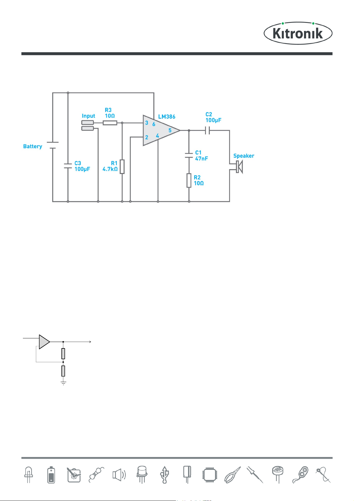
The kit is supplie with ½ a metre of twin cable with a 3.5mm Jack connector on one en .
This cable will be use to connect both the speaker an the MP3 player. You will nee to
cut a length from the en that oes not have the Jack connector on, which will be use to
connect the speaker in a later step. Make sure that you leave enough cable on the en with
the jack so that you have a long enough lea to connect your MP3 player!
Strip the insulation from the other en of the cable that has the Jack plug on. Run some sol er
onto the expose wire an trim the wire so that only 2 or 3mm of tinne wire is left. Sol er these
wires into the boar where it is labelle ‘Input’. It oesn’t matter which of the pair of wires goes
into each of the two pa s. The wires shoul be fe through the strain relief hole before being
sol ere into place.
Take the piece of wire that you previously cut from the jack lea an strip the en s of the wire.
Sol er one en to the two terminals on the speaker an the other en to the boar connection
marke ‘Speaker’. It oes not matter which way aroun these connections go. Again the wires
shoul be fe through the strain relief hole before being sol ere into place.
The IC can now be put into the hol er, ensuring the notch on the chip lines up with the notch on the hol er. Your
amplifier is rea y for use. You can use the volume control on your MP3 player to control how lou the amplifier is.
Just make sure that it’s mi volume when you test the amplifier.
Checking Your Amplifier PCB
Carefully check the following before you insert the batteries:
Audio equipment may become damaged if connected to an incorrectly built amplifier.
Check the bottom of the board to ensure that:
•All holes (except the 4 large (3 mm) holes in the corners) are fille with the lea of a component.
•All these lea s are sol ere .
•Pins next to each other are not sol ere together.
Check the top of the board to ensure that:
•The three wires are connecte to the right place.
•The ‘-’ on the capacitors match the same marks on the PCB.
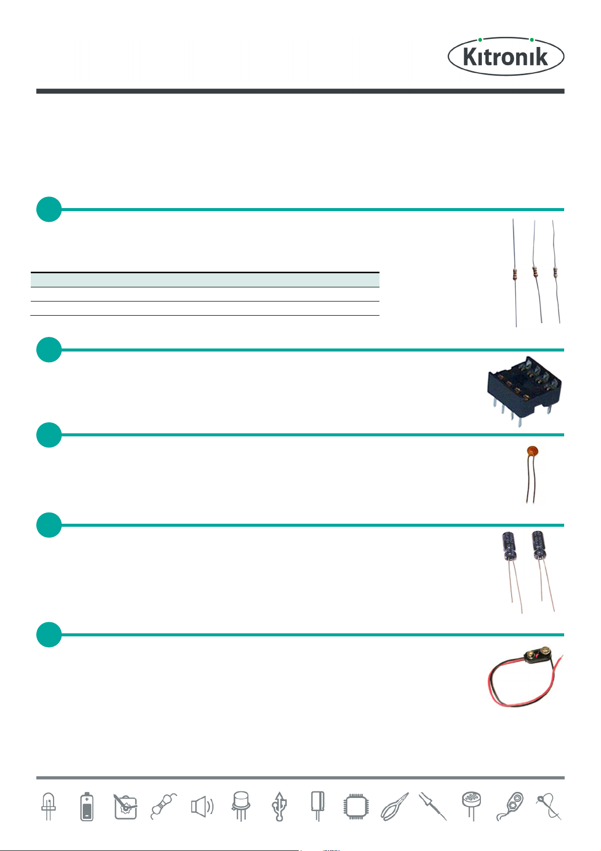
•The colour ban s on R1 are yellow, purple, re & R2 & R3 are brown, black, black.
•The battery clip re an black wires match the re & black text on the PCB.
•The notch on the IC is next to the power connection.
CONNECT THE JACK LEAD
7
CUT THE JACK LEAD
6
CONNECT THE SPEAKER
8
INSERTING THE IC INTO THE HOLDER
9

Mono Amplifier Essentials
www.kitronik.co.uk/2154
Adding an On / Off Switch
If you wish to a a power switch, on’t sol er both en s of the battery clip irectly into the boar , instea :
Sol er one en of the battery clip to the PCB, either black to ‘-‘ or re to ‘+’.
Sol er the other en of the battery clip to the on / off switch.
Using a piece of wire, sol er the remaining terminal on the on / off switch to the remaining
power connection on the PCB.
1
3

Mono Amplifier Essentials
www.kitronik.co.uk/2154
Fault finding flow chart
Is the speaker
making any kind
of sound?
Yes
No
Fault finding flow chart
Start
Power up the board with it
connected to a music source
Stop
Is the speaker
playing the music
clearly?
Check
• C2 is the right way around and
the joints are good
• R3 for dry joints
• IC pins 3 and 6 for dry joints
• Power leads correct way around
and for dry joints
• Input leads are correct way
around and for dry joints.
• Speaker leads for dry joints
Yes
Check
• R1& R2 for
dry joints
• C1for dry
joints
• C3 is right
way around
and for dry
joints.
No it’s
distorted
Is the
sound just a steady
frequency?
Check
• IC1 pin 4 for
dry joint
Yes
No

Mono Amplifier Essentials
www.kitronik.co.uk/2154
Designing the Enclosure
When you esign the enclosure, you will nee to consi er:
•The size of the PCB (below left, height inclu ing components = 15mm)
•How big the batteries are.
•How to mount the speaker (below right).
•How to allow the au io cable out of the box.
•Are you making the amplifier for a particular MP3 player, if so shoul the MP3 player go in the box?
These technical rawings of the amplifier PCB an speaker shoul help you plan this.
All dimensions in mm
x4 holes 3.3mm diameter
Mounting the PCB to the
enclosure
The rawing to the left shows
how a hex spacer can be use
with two bolts to fix the PCB
to the enclosure.
Your PCB has four mounting
holes designed to take M3
bolts.

Mono Amplifier Essentials
www.kitronik.co.uk/2154
How the Amplifier Works
At the centre of the circuit is an au io amplifier Integrate Circuit or IC. Insi e the IC are lots of transistors, which are
connecte together to allow the small input signal to be amplifie into a more powerful output that can rive a
speaker.
All amplifiers nee to use fee back to ensure the amount of gain stays the same. This allows the output to be an
exact copy of the input just bigger. The gain is the number of times bigger the output is compare to the input, so if
an amplifier has a gain of 10 an there is 1 volt on the input there will be 10 volts on the output. Before looking at
how the fee back works, we first nee to un erstan how a stan ar amplifier works. An operational amplifier has
two inputs these are calle the inverting (-) an non-inverting (+) inputs. The output of the operational amplifier is
the voltage on the non-inverting input less the voltage on the inverting input multiplie by the amplifiers gain. In
theory an operational amplifier has unlimite gain so if the non-inverting input is a fraction higher than the inverting
input (there is more + than -) the output will go up to the supply voltage. Change the inputs aroun an the output
will go to zero volts. In this format the operational amplifier is acting as a comparator, it compares the two inputs
an changes the output accor ingly.
With an infinite gain the amplifier is no goo to amplify au io, which is where the
fee back comes in. By making one of the input a percentage of the output the gain can
be fixe , which allows the output to be a copy of the input but bigger. Now when the
two inputs are compare an the output is a juste , instea of it going up or own
until it reaches 0 volts or V+, it stops at the point when the two inputs match an the
output is at the require voltage.
Looking at the circuit iagram for the au io amplifier it’s not obvious where the fee back is, this is because insi e
the IC there are resistors fixing the gain at 20.
The rest of the components are nee e as follows:
C3 is connecte across the supply to make sure that it remains stable.
The other capacitors have a filtering role, either to cut out high frequency noise or get the best out of the speaker.
Gain x10
90%
10%
Input Output
Amp

Online Information
Two sets of information can be ownloa e from the pro uct page where the kit can also be reor ere from. The
‘Essential Information’ contains all of the information that you nee to get starte with the kit an the ‘Teaching
Resources’ contains more information on sol ering, components use in the kit, e ucational schemes of work an so
on an also inclu es the essentials. Downloa from:
www.kitronik.co.uk/2154
Every effort has been ma e to ensure that these notes are correct, however Kitronik accept no responsibility for
issues arising from errors / omissions in the notes.
Kitronik Lt - Any unauthorise copying / uplication of this booklet or part thereof for purposes except for use
with Kitronik project kits is not allowe without Kitronik’s prior consent.
This kit is esigne an manufacture in the UK by Kitronik
Table of contents
Other Kitronik Amplifier manuals