Leader LTC-905 User manual

LEADER
CURVE
TRACER
INSTRUCTION
MANUAL

TABLE
OF
CONTENTS
Page
1.
DESCRIPTION
.
1
2.
SPECIFICATIONS
.
1
3.
CONTROLS
AND
CONNECTORS
.
1
4.
OPERATION
4.1
Preliminary
Notes
.
3
4.2
Preparation
.
5
4.3
Transistor
Measurements
..
5
4.3.1
NPN,
low
level
.
5
4.3.2
NPN,
power
type
.
6
4.3.3
PNP,
low
level
.
6
4.3.4
PNP,
power
type
.
6
4.3.5
Measurement
of
hpg
..
7
4.4
Measurement
of
FET’s..
..
8
4.4.1
N-cEannel
FET,
and
N-channel
MOS
FET..
8
4.4.2
P-channel
FET,
and
P-channel
MOS
FET
.
8
4.4.3
Mutual
conductance,
gm,
measurement
..
8
4.4.4
Enhancement
type
FET
measurement
.
9
4.5
Diode
Measurements
4.5.1
Standard
test
condition
.
9
4.5.2
General
purpose:
Power
rectifiers,
detectors
.10
4.5.3
Zener
diodes
.....10
4.5.4
Tunnel
diodes
...10
4.5.5
Quantitative
diode
measurements
...10
4.6
SCR
(Thyristor)
Measurements.H
4.7
UJT
(Unijunction
transistor)
Measurements.
j
j
5.
Measurements
with
External
Bias
5.1
General...
12
5.2
Transistor
Measurements
....
12
5.2.1
Bias
supplies
.
12
5.2.2
hpg
measurements.
5.2.3
IcEO
measurements
.
jg

5.3
F
ET
Measurements..
.
.
.
..
2
3
5.3.1
Bias
supplies
.13
5.3.2
gm'
measurements
.
1
4
5.3.3
Pinch-off
Voltage,
Vp,
measurement
.-.14
5.3.4
Drain
current,
measurement.15
6.
In-Circuit
Testing...j
5
6.1
General..
6.1.1
Application
.15
6.1.2
Use
of
In-Circuit
Probe,
LP-11
.15
6.2
Display
of
Defective
Transistors,
FET
.16
6.3
Notes
on
In-Circuit
Testing
.17
7.
MAINTENANCE.18
7.1
Removing
the
Panel
from
Case.18
7.2
Fuse
Renewal.18
7.3
AC
Input
Connections.18

1.
DESCRIPTION
Curve
tracing
on
a
scope
is
made
easy
with
the
LTC-905.
Characteristic
curves
of
all
types
of
semiconductors
can
be
accurately
displayed.
This
is
far
superior
to
the
conventional
ohmmeter
checks
for
quality.
In-circuit
testing
is
possible
for
quick
checks.
Two
inputs
are
provided
which
enable
comparison
of
two
similar
units.
LTC-905
is
designed
to
test
the
following:
1.
Transistors
-
NPN,
PNP,
FET
and
MOS
FET.
2.
SCR’s
(Thyristors)
and
Triacs.
3.
Diodes
-
rectifier,
detector,
zener
and
tunnel.
2.
SPECIFICATIONS
Collector/Drain
Sweep
Frequency
Voltage
Sweep
Waveform
Current
Current
Limiter
Step
Generator
No.
of
Steps
Current
per
Step
Volt
per
Step
External
Bias
Power
Requirements
Size
and
Weight
Accessories
120Hz,
or
100Hz
(2
x
line
frequency).
8
steps:
10,
20,
30,
40,
50,
60,
80
and
100V;
accuracy,
±10%.
(Rated
voltage)
Fullwave
rectified.
100mA,
maximum.
100012
for
low
level
transistors;
100S2
for
power
transistors.
7.
10,
20,
50/iA;
0.1,
0.2,
0.5,
1,
2mA;
accuracy,
±5%.
0.1,
0.2,
0.5V;
accuracy,
±5%.
One
curve
display.
100,
120,
200,
220,
or
240V,
50/60Hz,
25VA
maximum
operating,
and
6VA
at
standby.
240(W)X
90(H)X
170(D)
mm,
2kg,
(9^”X
3>f
X
6K”;
4.5
lbs.)
Instruction
manual
.
1
3-lead
cable
(banana
plugs/clips)
.
2
Scope
leads,
2
red
and
1
black
.1
set
In-circuit
test
probe,
LP-11
.
1
3.
CONTROLS
AND
CONNECTORS
®
POWER
switch
Turns
on
the
AC
power.
(D
Pilot
lamp
Indicates
when
AC
power
is
on.
(D
POLARITY
switch
Selects
the
mode
of
operation.
©
VERTICAL
jacks
Connections
to
vertical
scope
input.
©
EXT.
BIAS
jack
Connection
to
an
external
source
to
apply
base
or
gate
bias
for
a
one
curve
display.
i

©
BASE
CURRENT/
GATE
VOLTAGE
switch
(7)
Banana
plug
jacks
®
TO-5
socket
©
SELECTOR,
lower
©
SELECTOR,
upper
©
TO-5
socket
@
Banana
plug
jacks
@
COLLECTOR/DRAIN
SWEEP
VOLTAGE
switch
@
CURRENT
LIMIT
switch
©
H.
LENGTH
control
@
HORIZONTAL
jacks
Sets
the
bias
current
in
eight
steps
and
gate
voltage
in
three
steps;
provided
with
position
for
external
bias.
One
group
for
test
lead
connections:
Color
;
Transistor
FET
Blue
C
-
Collector
D-
Drain
Green
B
-
Base
G
-
Gate
Yellow
!
E
-
Emitter
S
-
Source
For
insertion
of
transistor
under
test.
Selects
input
at
“A”
or
“B”
side.
At
OFF,
both
sides
are
disconnected.
Setting
depends
on
type
of
transistor,
NPN
or
PNP
at
TRANS;
MOS
FET
and
FET
at
FET.
Same
as
®
.
Same
as
(7)
.
With
eight
positions
for
setting
the
sweep
voltage.
Set
at
SIGNAL
for
low
level
types
and
at
POWER
for
power
types.
Adjusts
the
amplitude
of
the
horizontal
sweep
on
the
scope.
Connections
to
horizontal
scope
input.
o

4.
OPERATION
4.1
Preliminary
Notes
A.
A
C
Line
Voltage.
The
AC
voltage
for
operation
should
be
kept
within
±10%
of
the
rated
value,
see
CHART
1.
When
low,
the
performance
will
be
affected;
when
high,
damage
may
result
to
circuit,
components
in
the
instrument.
CHART
1
Rating,
V
Range,
V
Fuse
100
90
-
110
120
108
-
132
200
180
-
220
0.5A
220
198
-
242
240
216
-
264
The
line
fuse
is
0.5A
for
all
voltages.
Refer
to
Sect.
7.3
for
primary
connections
when
different
voltages
are
used.
B.
A
C
Input
Phasing.
Unless
the
phase
of
the
AC
voltage
to
the
LTC-905
and
scope
are
in
proper
relation,
“double
curves”
will
be
displayed,
see
Fig.
4-1.
This
can
be
corrected
by
reversing
the
AC
plug
connection
on
the
scope
or
LTC-905.
NOTE:
When
the
scope
is
not
provided
with
the
DC
input
to
the
horizontal
amplifier,
the
proper
display
may
not
be
obtained.
Fig.
4-1
Double
curve
effect,
AC
phasing
not
proper.
C.
Collector
or
Drain
Sweep
Application.
In
order
to
protect
the
transistors
and
diodes
against
damage,
care
must
be
taken
in
application
of
the
sweep
voltage.
Voltages
over
10V
should
not
be
used
unless
specially
noted.
D.
Scope
Characteristics
The
scope
for
curve
tracing
is
used
as
an
X-Y
scope.
It
is
necessary
that
the
scope
satisfies
the
conditions
in
CHART
2.
3

CHART
2
i
Amplifier
Bandwidth
'
i
Sensitivity,
minimum
Vertical
DC
-
1kHz
or
higher
0.1V/cm,
or
/div.
Horizontal
DC,
or
AC
-
1kHz
or
higher
lV/cm,
or
/div.
In
quantitative
measurements,
particularly
for
hpp
and
g
m
,
a
scope
with
the
vertical
gain
calibrated
in
V/cm
should
be
used.
For
ease
in
readouts,
the
V/cm
sensitivities
converted
to
the
most
used
mA/cm
calibration
at
two
settings
of
the
CURRENT
LIMIT
switch
are
listed
in
CHART
3.
CHART
3
Vertical
Sensitivity
CURRENT
LIMIT
Setting
SIGNAL
POWER
i
50mV/cm
0.5mA/cm
5mA/cm
0.1
V/cm
1
mA/cm
10m
A/cm
0.2V/cm
!
2mA/cm
i
20mA/cm
0.5V/cm
!
5mA/cm
!
50mA/cm
By
adjusting
the
H.
LENGTH
control
for
the
trace
to
cover
10cm,
the
V/cm
unit
horizontally
can
be
correlated
with
the
sweep
voltage
setting.
E.
Scope
Connections
and
Settings.
Connections
between
the
scope
and
LTC-905
are
made
with
the
three
leads
as
indicated
in
Fig.
4-2,
red
leads
to
vertical
and
horizontal
inputs
and
black
lead
to
common
ground.
Set
the
vertical
gain
initially
at
lOOmV/cm
and
the
AC-DC
switch
at
DC.
Set
the
horizontal
gain
at
maximum
and
the
AC-DC
switch
at
DC
(use
AC
coupling
if
DC
is
not
provided).
4

4.2
Preparation
Switch
settings:
POWER
CURRENT
LIMIT
COLLECTOR/DRAIN
SWEEP
VOLTAGE
BASE
.
GATE
CURRENT'VOLTAGE
SELECTOR:
upper
lower
OFF.
SIGNAL.
10
V.
EXT
BIAS
Type
under
test,
TRANSistor
or
FET.
OFF.
Connections:
With
proper
attention
to
the
terminals,
the
transistor
is
connected
to
the
socket
or
leads
from
the
three
jacks
at
“A”
or
“B”
side.
When
comparing
two
units,
use
the
sockets
and
lead
connections
at
both
sides.
4.3
Transistor
Measurements
4.3.1
NPN,
low
level.
Switch
settings:
BASE
CURRENT
COLLECTOR
SWEEP
POLARITY
CURRENT
LIMIT
SELECTOR:
upper
lower
10
(lA.
10V.
NPN.
SIGNAL.
TRANS.
A
or
B,
as
connected.
The
scope
controls
are
adjusted
for
suitable
display
and
proper
positioning,
see
Fig.
4-3
and
Fig.
4-4.
Seven
curves
will
be
observed
with
Si
transistors
and
eight
curves
with
Ge
transistors.
This
serves
as
a
check.
When
the
BASE
CURRENT
is
set
at
20juA,
the
height
will
be
doubled.
The
transistor
can
be
said
to
be
satisfactory
when
the
curves
are
displayed
as
shown
in
the
figures.
5

4.3.2
NPN,
power
type.
For
NPN
power
transistors,
under
the
same
conditions
as
in
Sect.
4.3.1,
set
the
CURRENT
LIMIT
at
POWER
and
BASE
CURRENT
at
0.1
up
to
1mA.
As
the
COLLECTOR
SWEEP
VOLTAGE
is
gradually
raised
from
10V
upward.
Do
not
increase
the
sweep
voltage
beyond
the
point
where
the
curves
start
to
bend,
the
curves
will
be
as
shown
in
Fig.
4-5.
The
region
of
the
breakdown
voltage
can
be
read
off.
For
example,
with
the
sweep
voltage
at
50V,
adjust
the
H.
LENGTH
control
for
the
sweep
to
cover
10cm
horizontally,
Fig.
4-5
Power
transistor
°
r
5V/cm
’
in
this
case
-
The
collector-emitter
voltage,
V
CE
,
„>
can
be
read
easily,
curves.
The
curves
1
start
to
bend.
By
adjusting
the
H.
LENGTH
control
for
the
trace
to
cover
10cm
(or
div.),
the
V/cm
unit
can
be
correlated
with
the
voltage
settings.
NOTES.
1.
When
the
sweep
voltage
and/or
base
current
are
increased,
the
transistor
will
become
heated.
2.
Power
transistors
should
be
tested
within
as
short
a
time
as
possible.
This
will
prevent
overheating
when
the
sweep
voltage
is
over
10V
and/or
when
a
large
base
current
is
flowing.
4.3.3
PNP,
low
level.
Switch
settings:
BASE
CURRENT
COLLECTOR
SWEEP
POLARITY
CURRENT
LIMIT
SELECTOR:
upper
lower
10/uA.
10V.
PNP.
SIGNAL.
TRANS.
A
or
B,
as
connected.
The
curve
tracing
procedure
is
the
same
as
given
in
Sect.
4.3.1.
The
curve
display
will
be
as
shown
in
Fig.
4-6.
Fig.
4-6
PNP
transistor
curves.
4.3.4
P
NP,
power
type.
Set
the
switches
as
in
Sect.
4.3.2
above
with
the
following
exception:
POLARITY
at
PNP.
The
curve
tracing
procedure
is
the
same
as
described
for
NPN
power
transistors.
The
same
care
must
be
exercised
to
prevent
overheating
with
high
sweep
voltages
and
base
currents.
6

4.3.5
Measurement
of
hpg.
Measurement
of
h
FE
for
an
NPN
transistor
will
be
given;
for
the
PNP
type,
the
only
changes
will
be
in
the
setting
of
the
POLARITY
switch
at
PNP
instead
of
NPN
Ind
in
the
direction
of
the
curves.
The
DC
current
amplification
of
a
transistor
is
given
by
the
relation
-
Collector
current,
Ip
h
FE
=
---
Base
current,
Ig
For
this
measurement,
a
calibrated
scope
is
required.
Referring
to
CHART
3
(Sect.
4.1,
Parag.
D)
under
SIGNAL
of
CURRENT
LIMIT,
the
vertical
gain
is
set
at
O.lV/cm.
Under
this
condition,
the
collector
current
is
read
off
at
ImA/cm.
With
the
Si
transistor,
seven
typical
curves
for
Ig
in
lOfiA
steps
from
0
to
60/iA
are
shown
in
Fig.
4-7.
On
the
60/tA
curve,
I
c
=
4.2mA.
By
calculation,
h
FE
=
4.2
x
10'
3
/
60
x
10*
6
=
70.
In
Fig.
4-8,
curves
for
a
typical
Ge
transistor
are
shown.
From
the
I
fi
=
70/1
A,
I
c
=
2.1mA
and
hpg
=
30.
Fig.
4-8
hp
E
measurement,
Ge
transistor.
In
the
two
examples
given
above,
hpg
measurements
are
collector-emitter
voltage,
V^g
=
10V.
Other
measurements
can
be
made
when
required
with
the
sweep
voltage
at
20,
30V,
etc.
For
hpg
of
power
transistors,
set
the
CURRENT
LIMIT
switch
at
POWER
and
the
POLARITY
switch
at
NPN
or
PNP
as
required.
The
scope
sensitivity
is
set
by
reference
to
the
POWER
column
of
CURRENT
LIMIT
in
CHART
3.
For
example,
with
the
sensitivity
at
0.2V/cm,
the
calibration
will
be
20mA/cm.
By
setting
the
BASE
CURRENT
at
0.2mA,
and
SWEEP
VOLTAGE
at
50V
(10cm
length),
curves
in
Fig.
4-9
will
be
displayed.
From
the
figure,
Ig
=
1.2mA
and
I
c
=
50mA.
Thus,
hpg
is
approximately
41.7.
Measurements
of
hpg
in
this
manner
will
be
accurate
within
+10%.
For
higher
accuracy,
use
an
external
bias
supply;
details
are
given
in
Sect.
5.
Fig,
4-9
hpg
measurement,
power
transistor.
7

4.4
Measurement
of
FET’s
4.4.1
N
-channel
FET,
and
N-channel
MOS
FET.
Switch
settings:
GATE
VOLTAGE
DRAIN
SWEEP
POLARITY
CURRENT
LIMIT
SELECTOR:
upper
lower
0.1V.
10
V.
N-CHAN.
SIGNAL.
FET.
A
or
B,
as
connected.
Eight
curves
will
be
displayed
as
shown
in
Fig.
4-10.
As
the
sweep
voltage
is
increased,
the
upper
operating
limits
will
be
approached,
see
Fig.
4-11.
4.4.2
P
-channel
FET,
and
P-channel
MOS
FET.
Set
the
POLARITY
switch
at
P-CHAN.
Other
switch
settings
are
the
same
as
in
Sect.
4.4.1
above.
Fig.
4-12
shows
the
curve
display.
Fig.
4.-12
Curves
for
P-channel
FET
and
P-channel
MOS
FET.
4.4.3
M
utual
conductance,
gm,
measurement.
The
gm
measurement
for
the
N-channel
FET
will
be
described;
for
the
P-channel
FET,
the
only
changes
will
be
in
the
setting
of
the
POLARITY
switch
at
P-CHAN
instead
of
N-CHAN,
and
the
curve
direction.
8

In
the
FET,
mutual
conductance
defined
by
the
relation
-
_
AI
D
g
m
_
—
a
t
constant
Vjyc.
AV
GS
The
switch
settings
are
the
same
as
given
in
Sect.
4.4.1.
The
CURRENT
LIMIT
switch
is
set
at
SIGNAL;
the
scope
is
set
at
O.lV/cm
sensitivity.
Under
this
condition,
the
drain
current
will
be
calibrated
at
ImA/cm.
The
GATE
VOLTAGE
is
set
at
0.1V
and
trace
length
at
10cm.
In
Fig.
4-13,
eight
curves
are
shown
between
V
GS
=
0
to
0.7V.
On
the
graticule,
the
drain
current
between
these
two
voltages
are
read
off.
From
the
figure,
the
change
in
Iq
is
2.1mA,
and
gm
2.1
x
10~
3
0.7
-
3
x
10
3
,
or-
3
millimhos.
Fig.
4-13
gm
measurement
in
FET.
4.4.4
Enhancement
type
FET
measurement.
There
are
two
types
of
the
MOS
FET,
depletion
and
enhancement.
Measurements
hitherto
described
relate
to
the
N-channel
FET
of
the
depletion
type
wherein
the
drain
current,
Ip,
decreases
when
the
gate-source
voltage,
V
G
g,
is
increased.
In
the
enhancement
type,
there
is
practically
no
drain
current
when
V
G
g
is
zero
but
will
increase
when
VG
g
is
applied
in
the
positive
direction.
Consequently,
when
testing
the
enhancement
type,
the
upper
SELECTOR
switch
must
be
set
at
TRANS.
This
will
provide
bias
with
the
correct
polarity.
Other
switch
settings
are
the
same
as
given
in
Sect.
4.4.1.
4.5
Diode
Measurements
4.5.1
Standard
test
condition.
Switch
settings:
COLLECTOR/DRAIN
SWEEP
POLARITY
CURRENT
LIMIT
SELECTOR:
upper
lower
10V.
DIODE
FORWARD.
SIGNAL.
Any
setting.
A
or
B,
as
connected.
9

/
GATE
VOLTAGE
Any
setting.
BASE
CURRENT
Connections:
The
diode
under
test
is
connected
to
the
tracer
as
follows:
anode
to
collector
jack
and
cathode
to
emitter
jack,
as
shown
on
the
panel
marking
at
the
A
or
B
side.
4.5.2
G
eneral
purpose:
Power
rectifiers
and
detectors.
Curves
are
shown
in
Fig.
4-14
for
two
characteristics,
depending
on
the
POLARITY
switch
settings,
namely,
DIODE
FORWARD
and
DIODE
BACKWARD.
For
the
diode
in
good
condition,
the
forward
characteristic
will
be
as
shown.
Fig.
4-14
Diode
characteristics.
4.5.3
Z
ener
diodes.
Under
the
standard
test
condition,
set
the
POLARITY
switch
at
DIODE
BACKWARD.
The
curve
displayed
will
be
as
shown
in
Fig.
4-15.
Depending
on
the
characteristic,
the
sweep
voltage
can
be
increased
to
20V
or
higher
as
required.
By
setting
the
POLARITY
switch
at
DIODE
FORWARD,
the
trace
indicated
with
the
dashed
line
will
be
displayed.
Fig.
4-15
Zener
diode
characteristics.
4.5.4
T
unnel
diodes
Under
the
standard
test
condition,
Sect.
4.5.1
above,
the
curve
will
be
displayed
as
shown
in
Fig.
4-16.
Fig.
4-16
Tunnel
diode
characteristics.
The
curve
at
the
right
of
the
0V
axis
with
the
polarity
switch
at
DIODE
FORWARD.
There
will
be
a
blank
in
the
curve
(dashed
part.)
which
is
the
negative
resistance
characteristic.
The
curve
at
the
left
of
0V
axis
will
be
displayed
when
the
switch
is
set
at
DIODE
BACKWARD.
4.5.5
Q
uantitative
diode
measurements
By
calibrating
the
horizontal
axis
in
V/cm,
the
current/voltage
characteristic
can
be
determined.
Set
the
trace
length
horizontally
at
10cm.
This
will
calibrate
the
sweep
voltage
at
1/10
(one-tenth)
of
the
switch
setting.
For
example,
if
set
at
10V,
then
1cm
is
equivalent
to
IV.
With
use
of
the
calibrated
vertical
scale,
the
forward
“rise”
in
diodes,
zener
breakdown
voltage,
etc.,
can
be
determined
readily.
10

11

Curves
for
the
UJT
are
shown
Fig.
4-20.
Since
the
curves
will
be
close
together,
set
the
H.
LENGTH
control
to
full
clockwise
for
spreading.
Fig.
4-20
UJT
characteristics.
5.
MEASUREMENTS
WITH
EXTERNAL
BIAS
5.1
General
A
single
curve
will
be
displayed
when
an
external
bias
is
applied
to
the
transistor
under
test.
Accurate
measurements
of
hpg
and
g
m
are
possible.
The
bias
current
or
voltage
source
is
connected
to
the
EXT
BIAS
jacks.
The
BASE
CURRENT/GATE
VOLTAGE
switch
is
set
at
EXT
BIAS.
5.2
Transistor
Measurements
5.2.1
Bias
supplies.
Circuits
for
supplying
the
external
bias
to
the
NPN
and
PNP
transistors
are
shown
in
Fig.
5-1
and
Fig.
5-2.
The
source,
battery
or
regulated,
should
be
in
the
1
to
5V
range;
in
most
measurements,
a
1.5V
cell
is
sufficient.
The
variable
resistor
VR,
about
50kf2,
is
used
to
adjust
the
current.
A
DC
microammeter,
100
to
500/rA,
will
be
suitable
in
most
measurements.
For
power
transistors,
the
range
should
be
1
to
5mA.
5.2.2
hpp
measurements.
Switch
settings:
BASE
CURRENT
SWEEP
VOLTAGE
CURRENT
LIMIT
SELECTOR:
upper
lower
POLARITY
EXT.
BIAS.
10V.
SIGNAL.
TRANS.
A
or
B,
as
connected.
NPN
or
PNP,
depending
on
the
transistor.
The
scope
sensitivity
is
set
at
O.lV/cm
for
calibration
at
ImA/cm.
Adjust
the
bias
current
with
VR.
12

The
curve
for
an
NPN
transistor
will
be
as
shown
in
Fig.
5-3.
For
example,
if
the
bias
current,
Ig,
is
set
at
50/lA
and
collector
current,
Iq,
is
4mA
(see
curve),
then
AI
C
4mA
4
x
10'
3
"FE
~
'
,
T
=
-
=
-
=
80.
ai
B
50
/uA
50
x
10"
6
The
hpg
can
be
measured
at
different
values
of
Ig
with
adjustment
of
VR.
For
power
transistors,
set
the
CURRENT
LIMIT
switch
at
POWER
and
follow
the
same
procedure.
For
PNP
transistors,
set
the
POLARITY
switch
at
PNP;
the
curve
will
inverted.
Disconnect
the
EXT
BIAS
connection,
the
I^go
is
measured.
(External
bias
is
not
used.)
Fig.
5-4
shows
the
curve
for
a
Ge
type
transistor
where
the
lego
*
s
relatively
high.
Fig.
5-4
IcEO
measurement,
Ge
transistor.
5.3
FET
Measurements
5.3.1
Bias
Supplies.
The
bias
voltage,
Vq^,
supplies
for
N-channel
and
P-channel
FET’s
are
shown
in
Fig.
5-5
and
Fig.
5-6.
The
output
is
connected
to
the
EXT
BIAS
jacks
as
indicated.
The
source,
battery
or
regulated,
should
be
in
the
3
to
6V
range.
A
lk£2
potentiometer,
VR,
and
a
suitable
voltmeter
are
required.
13

5.3.2
gm
measurements.
Switch
settings:
POLARITY
N-CHAN
or
P-CHAN,
depending
on
FET.
GATE
VOLTAGE
EXT
BIAS.
SWEEP
VOLTAGE
10V.
CURRENT
LIMIT
SIGNAL.
SELECTOR:
upper
FET
lower
A
or
B,
as
connected.
The
scope
sensitivity
is
set
at
O.lV/cm
for
calibration
at
ImA/cm
to
read
I
D
and
for
V
DS
at
IV/cm
with
the
H.
LENGTH
control.
Procedure:
1.
Note
the
Id(
0
)
reading
at
OV
bias
on
the
Vq§
=
OV
curve;
the
reading
is
taken
where
the
curve
flattens
out,
see
Fig.
5-7.
2.
Next,
set
the
bias
at
—0.5V
and
read
Id(—
0.5V)
on
t
^
ie
^GS
=
—
1
0.5V
curve.
3.
The
gm
is
defined
as
follows:
ai
d
8m
=
AV
GS
where
Al
D
=
I
D
^
0
j
-
I
D
(-0.5V),
and
AV
gs
=
OV
-
(—0.5V)
=
0.5V
Then
gm
^(0)
-
lD(-0.5V)
mA
05V
in
millimhos.
In
the
above
explanation,
steps
were
given
for
gm
measurement
at
^GS
=
an
d
—0.5V.
Other
measurements
can
be
made
with
different
values
of
Vqj.
For
the
P-channel
transistors,
the
curves
will
be
inverted.
Fig.
5-7
hpE
measurement
N-channel
FET.
5.3.3
Pinch-off
voltage,
Vp,
measurement.
Fig.
5-8
princh-
off
voltage
measurement.
An
example
will
be
given
for
the
N-channel
FET.
The
switches
and
scope
controls
are
set
as
given
in
Sect.
5.3.2.
Using
the
bias
source,
Fig.
5-5,
the
voltage
from
0V
is
increased
in
the
minus
direction.
Curves
will
appear
in
the
direction
indicated
by
the
arrow
in
Fig.
5-8.
As
more
negative
voltage
is
applied,
the
curve
becomes
straight.
The
bias
voltage
measured
at
this
point
is
the
Pinch-off
voltage,
Vp.
14

5.3.4
Drain
current,
Ijygg,
measurements.
An
N-channel
FET
will
be
used
in
the
following
example.
Disconnect
the
EXT
BIAS
connection
and
short
the
jack
to
ground.
(External
bias
is
not
used.)
The
switches
and
scope
controls
are
set
as
given
in
Sect.
5.3.2.
The
curve
for
I
DSS
is
shown
in
Fig.
5-9.
I
DS
§
is
read
off
at
the
point
indicated
with
the
arrow
in
the
figure.
In
general,
the
current
is
measured
with
V
DS
at
10V
and
so
the
sweep
voltage
is
set
at
20V.
For
FET’s
with
high
current,
set
the
scope
sensitivity
at
0.2V/cm
for
the
2mA/cm
calibration.
Fig.
5-9
^DSS
measurement.
6.
IN-CIRCUIT
TESTING
6.1
General
6.1.1
Application.
A
valuable
feature
of
the
LTC-905
lies
in
its
ability
to
test
and/or
compare
transistors
which
are
wired
in
TV
receivers,
radios
and
other
electronic
equipment.
Tests
for
quality
are
made
by
reference
to
the
instructions
given
for
transistors
in
the
relevant
sections
on
operation,
PRECAUTIONS:
1.
For
in-circuit
testing,
always
turn
off
the
operating
power,
AC
or
battery,
to
the
equipment.
2.
Confirm
the
type
of
transistor
before
testing
by
reference
to
the
schematic
or
a
handbook.
3.
To
prevent
possible
damage
to
the
transistor
and
other
circuit
components,
do
not
use
more
than
10V
for
the
sweep
voltage.
6.1.2
Use
of
In-Circuit
Probe,
LP-11
Instead
of
clips
used
in
testing
transistors
and
FET’s
which
are
mounted
on
circuit
boards,'
the
LP-11
Probe
will
be
found
very
handy.
The
banana
plugs
are
inserted
in
the
panel
jacks
according
to
the
color.
There
are
three
sharp
prods
equipped
with
swivel
joints
on
the
probe
head.
It
will
be
noted
that
two
prods,
blue
for
collector
(drain)
and
yellow
for
emitter
(source)
are
slightly
longer
than
the
green
prod
for
base
(gate).
In
use,
after
checking
the
proper
terminals
on
the
circuit
board,
the
two
longer
prods
are
connected
first
and
the
shorter
prod
is
“bridged”
for
the
connection.
Sharp
prods
are
used
to
pierce
the
insulation
on
the
solder.
For
safety,
always
put
the
cover
over
the
prods
after
use.
15

6.2
Display
of
Defective
Transistors,
FET’s
The
conditions
and
typical
displays
of
defective
transistors
and
FET’s
will
be
given
in
this
section.
1.
Base-collector
shorted
in
transistors.
Two
displays
are
shown
for
the
NPN
type
with
base
currents
at
10/t
A
and
0.2mA
in
Fig.
6
1
and
Fig.
6-2.
For
the
PNP
type,
the
curves
will
be
reversed
in
each
figure.
Fig.
6-1
Fig.
6-2
2.
Drain-gate
shorted
in
FET’s.
In
Fig.
6-3
and
Fig.
6-4,
two
conditions,
with
eight
curves,
are
shown
for
the
N-
channel
FET
with
gates
voltages
are
0.1V
and
0.5V.
3.
Fi
S-
6-3
Fig.
6-4
Collector-emitter,
or
Drain-source,
shorted,
or
total
short.
Only
a
vertical
line
will
be
displayed,
above
(PNPj
or
below
(NPN)
the
see
Fig.
6-5.
zero
axis,
16

4.
Base-emitter,
or
Gate-source,
Shorted
or
total
open.
This
condition
is
shown
in
Fig.
6-6
where
there
is
no
indication
of
the
base
current,
or
gate
voltage.
Fig.
6-6
6.3
Notes
on
In-Circuit
Testing
The
shape
of
the
displayed
curves
will
be
affected
by
presence
of
associated
circuit
components.
However,
it
may
be
assumed
that
the
transistor
or
FET
is
satisfactory
when
a
plurality
of
curves
is
displayed.
For
example,
typical
curves
for
an
NPN
transistor
in
circuit
are
shown
in
Fig.
6-7.
It
will
be
seen
that
when
the
base
current
is
increased,
there
will
be
considerable
distortion
in
the
curves.
Fig.
6-7
In-circuit
curves
for
NPN
transistor.
In
testing
transistors,
when
only
one
curve
is
displayed,
increase
the
base
current
from
10/tA
to
20(1
A
or
50(xA.
Typical
curves
for
different
base
currents
are
shown
in
Fig.
6-8.
Fig.
6-8
Effect
of
increasing
the
base
current.
For
FET’s,
increase
the
gate
voltage
from
0.1V
to
0.2V.
When
it
is
difficult
to
ascertain
whether
the
unit
defective,
it
should
be
tested
after
removal
from
the
circuit
board.
17
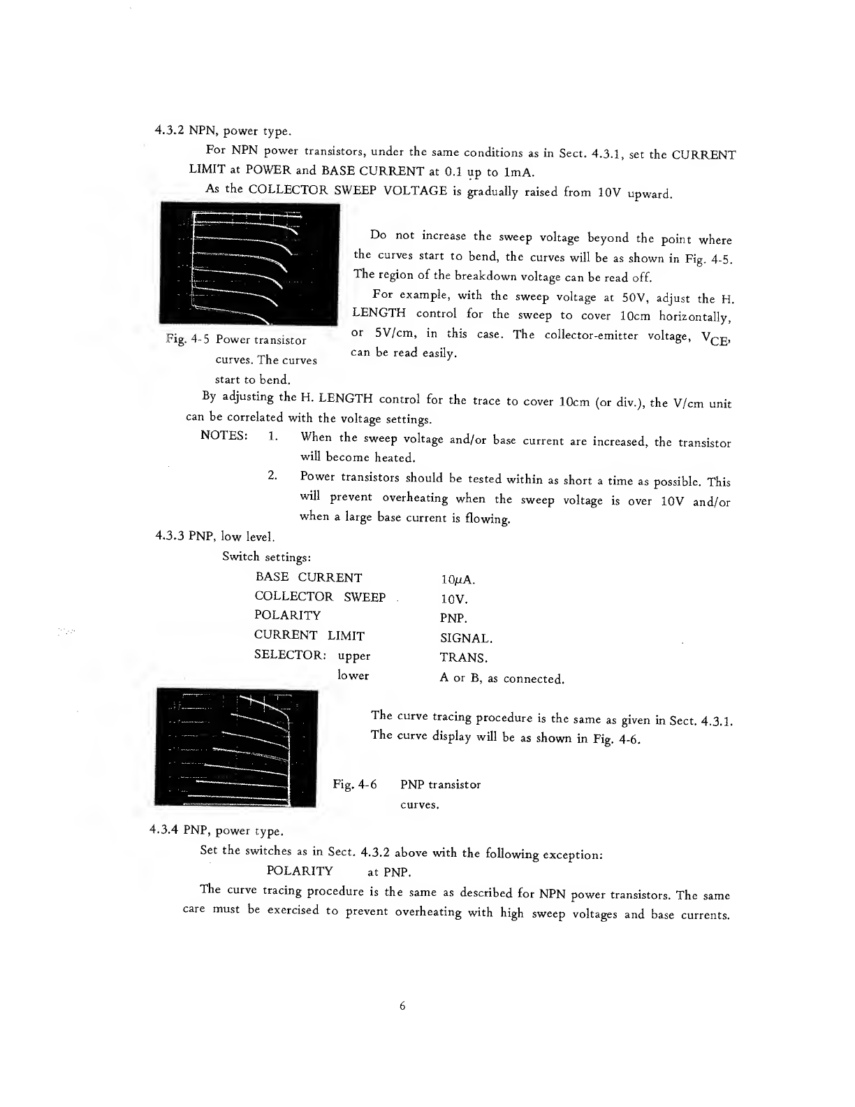
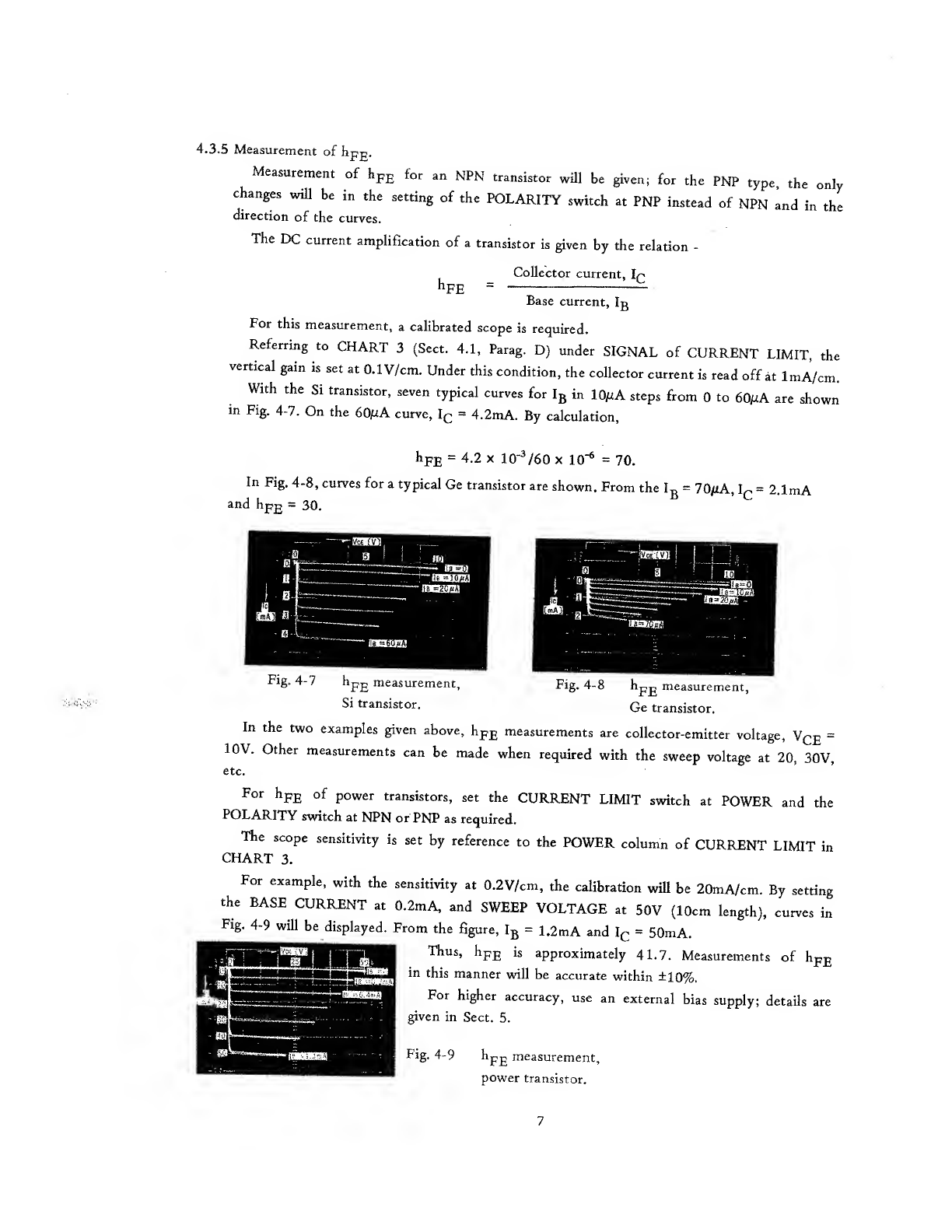
Other manuals for LTC-905
1
Table of contents
Other Leader GPS manuals