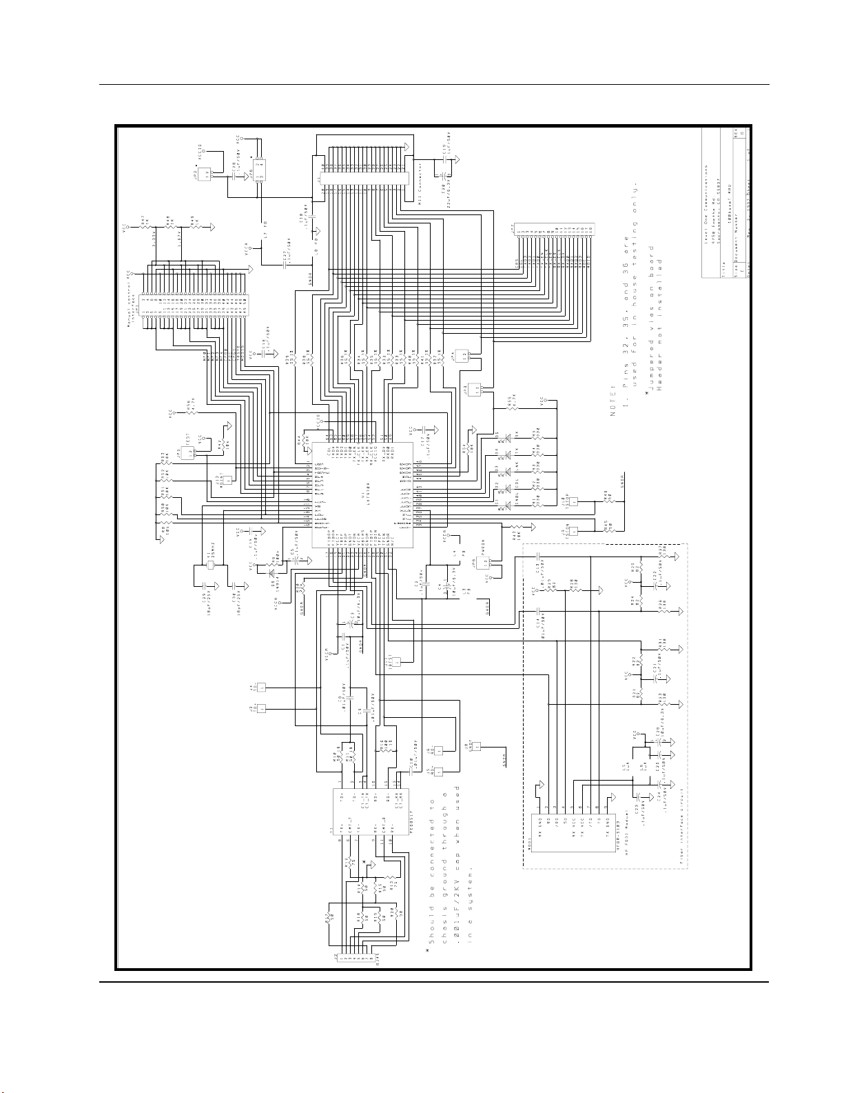
LXD970A Demo Board for 10/100 and 100BASE-FX applications
2
EQUIPMENT AND SETUP
The LXD970A Demo Board includes all the components
needed for a successful evaluation. However, the
following additional equipment is recommended:
• NetCom System X-1000 transceiver test box
configured with firmware version 1.17 or newer.
• PC with Fast Ether Windows (version 1.5 or newer)
installed.
• Various lengths of Category 5 Unshielded Twisted-
Pair (UTP) cable (1, 20, 40, 60, 80, 100, 120 and 140
meters).
• For 100BASE-FX evaluation, a fiber-optic
transceiver module (HFBR-5103) and fiber-optic
cable are required.
Test Setup
Figure 1 shows a typical test setup for the basic operation
of the LXD970A. The LXD970A plugs directly into a
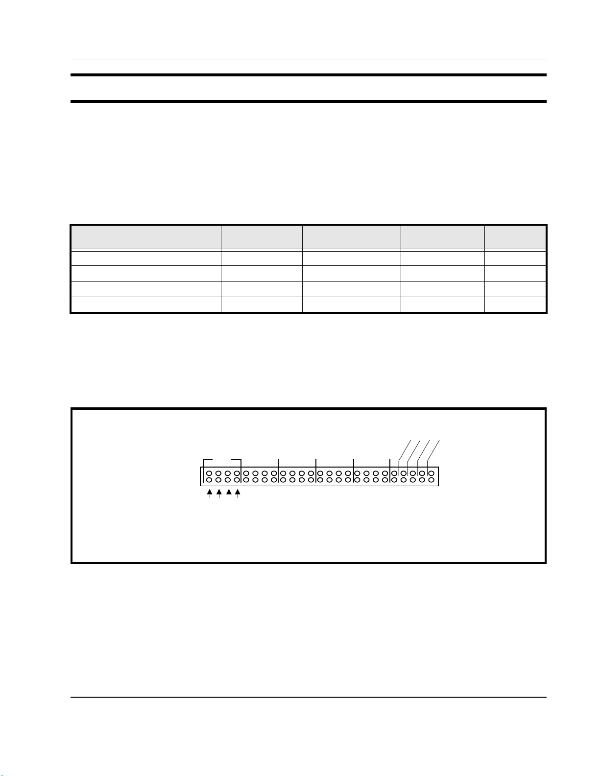
X1000 NetCom Transceiver TestBox via a standard40-pin
MII connector that is included on the board.
An optional test setup is shown in Figure 2 using a PC for
testing additional nodes.
Note: JP3 and JP4 must be installed on the LXD970A for
the Netcom System X-1000 transceiver test box to access
the MII management registers inside the LXT970A.
Figure 1: Basic Test Setup
Loading Test File
A disk that contains the file needed for testing is included
with the LXD970A demo board.
This file contains “Killer Packets” (100Tx4.s), that exhibit
worst case baseline wander characteristics suitable for
evaluating link performance and comparing the LXT970A
to alternative products. Some devices do not adjust well
over a range of cable distances. It is recommended to
compare LXT970A performance to similar devices over a
wide range of cable lengths.
Follow this simple procedure for loading test file into the
Netcom X-1000 test box:
• Load disk containing test pattern into computer
• Start Fast Ether Windows
• Click the “DATA PATTERN” button in the lower left
of the screen
• From the Data Pattern options presented, select
“CUSTOM”
• From the File menu, select “OPEN”, then select the
drive and directory where the test file is located. (If
you are using the disk from Level One, select
A:\100Tx4.s)
• When the test file is displayed on screen, select
“CLOSE”. This will automatically download the test
pattern to the Netcom X1000 test box
• Proceed with normal testing
Figure 2: Optional Test Setup
NETCOM
X1000
LXD970A
LXD970A
Serial
HUB
Port 1
Port 2
FAST ETHER
Windows
Terminal SW
RS232
RS232
UTP
UTP
RJ45
MII
PC
PC
NETCOM
X1000
LXD970A
LXD970A
UTP
Loop
MII
FAST ETHER
Windows
RS232
PC