LevelOne LXT970A User manual

LXT970A NIC Demo Board
with DEC 21143 Controller
JANUARY 1999
User Guide
General Description Features
Revision 1.4
The LXT970A NIC Demo Board provides a complete
working platform for evaluation of the LXT970A Fast
Ethernet Transceiver interfacing with the DEC 21143 LAN
Controller in a 10BASE-T and/or 100BASE-TX
environment.
The NIC Demo Board can be configured to operate in 10/
100Mbps (4B) Nibble Mode or (5B) Symbol Mode. This
document describes typical Demo Board setup procedures
for a 100BASE-TX environment. The NIC Demo board is
designed to plug directly into a PC and includes the driver
software required for the controller interface. LXT970A
NIC Demo Board is operated with a single 5V power
supply.
A complete Bill of Materials and schematics are included
for reference.
Before using the NIC Demo Board, review the latest
LXT970A Fast Ethernet Transceiver data sheet for the
most current information.
• Quick setup and ease of use for complete system
demonstration
• LXT970A Fast Ethernet Transceiver
• DEC 21143-PB LAN Controller
• Netware Driver software included
• Configurable for:
10Mbps / 100Mbps operation
(4B)Nibble Mode / (5B)Symbol Mode operation
• Single RJ45 connection
• LED indicators for major functions
• Standard half duplex or full duplex operation at 10 or
100Mbps
JP9
J2
TRANSFORMER
LXT970A
ENBL COL LNK TX RX DPX
DEC
21143-PB
U3
MF1
MF2
MF3
MF4
MF0
CFG0
FDE
CFG1
TRST
MDDIS
u
U7
U1
D1 D2 D3 D4 D5 D6
U5 U6
Y1
U8
T1
U2
JP7
JP8
J10
u
U4JP2
JP4
JP3
JP5
JP6
u u u uu
LXT970A DEMO/DEC21143

LXT970A NIC Demo Board with DEC 21143 Controller
2
EQUIPMENT SETUP
Equipment Requirements
The LXT970A NIC Demo Board includes all the
components needed for successful evaluation. However,
the following additional equipment is recommended:
•PCwithPCIbus
• Category 5 Unshielded Twisted-Pair (UTP) cable
The LXT970A NIC Demo Board is designed with a DEC
21143 PCI/CardBus 10/100Mbs Ethernet LAN Controller.
DEC 21143 Driver software must be installed to operate
the Controller. For more information on the 21143
Controller refer to Digital Semiconductor 21143 Data
Sheet.
Power Supply
The LXT970A NIC Demo Board is operated with a single
5V supply. The voltage is stepped down to 3.3V via a
voltage converter (U8) to operate the DEC 21143
Controller and the LXT970A MII.
Software Installation
Important: This installation procedure is valid for
users of Novell Personal Netware software only.
DEC 21143 Driver Software is included in the LXT970A
NIC Demo Board Kit. DC21X4.COM is the driver for the
DEC 21143 Controller. This file must be installed on a PC
to operate the Demo Board.
Installation of this software will overwrite all critical files
in the current configuration. Before installing driver
software make provisions to restore your computer to
“before installation” configuration by backing up all the
files found on the 21143 Driver Software Disk.
Files included on the disk are:
• DC21X4.cli
• DC21X4.com
• DC21X4.hdi
• DC21X4.ins
• IPXODI.com
• LSL.com
• NET.cfg
• Startnet.bat
•Vtm.exe
• Readme.txt
The software disk was shipped with write protection
engaged. Ensure the write protection of the disk is engaged
by verifying the two square holes at the top of the disk are
exposed. You can write protect the file by sliding the tab
up manually on the left side at the rear of the disk jacket.
The following steps are recommended for installation of
DEC 21143 Driver Software:
1. Make a copy of the files on the 21143 Driver Software
Disk for safe keeping.
2. Install the disk containing the 21143 Driver Software
in the Floppy (A:) Drive.
3. After boot-up, use DOS “CD” command, and change
the directory to C:\NWCLIENT.
Type: (cd c:\nwclient)
4. Move to floppy disk (A:) drive.
Type: (A:\)
5. Using DOS “CD” command, change directory to
A:\NOVELL.
Type:
(cd a:\novell)
6. Using DOS “COPY” command, copy the files
necessary to get the system running into the
C:\NWCLIENT directory.
7. Observe status messages from computer to insure
there are no copy errors, and that all files are copied.
8. Restart the computer. Your card should load
automatically during re-boot.
9. You may now edit your NET.CFG file to customize
your network environment. Additional commands and
explanations are included in the NET.CFG file itself.
From the NWCLIENT directory (step 3):
Type: (edit net.cfg)
The editor will open with NET.CFG loaded. Make
your edits and save the changes.

3
LXT970A NIC Demo Board Equipment Setup
Hardware Setup
The LXT970A NIC Demo Board can be configured for
(4-bit) Nibble Mode (Normal MII operation) or (5-bit)
Symbol Mode operation. Set jumpers (JP2 - JP9) for the
desired operating mode as shown in Table 1.
Hardware Installation
The LXT970A NIC Demo Board is designed to plug
directly into any PC. Basic instructions for installation and
network connection are as follows:
• Take the cover off the PC chassis.
• Install the LXT970A NIC Demo Board into an empty
PCI slot (Note: The PC must be turned OFF when
installing or removing the LXT970A NIC Demo
Board).
• Connect the LXT970A NIC Demo Board to the
Novell Network using CAT 5 Ethernet cable via the
RJ45 connector.
• Connect the metal shield of the RJ45 connector to
chassis ground. (This is required for ESD or EMI
testing.
•TurnON
the PC and verify the drivers are loaded
properly (If a problem occurs check the jumper
settings and the “Startnet.bat” and “net.cfg” files).
LED Indicators
There are 6 status LEDs on the LXT970A NIC Demo
Board. Refer to Table 2 for LED descriptions.
Table 1: LXT970A NIC Jumper Setup
Mode
Selection Jumpers Jumper Pin
Placement
Nibble Mode JP2 Pins 2 and 3
(Normal MII JP3
Operation) JP4
(4-bit) JP5
JP6
JP7
JP8 Pins 1 and 2
JP9 Pins 5 and 6
Pins 15 and 16
Pins 23 and 24
Pins 31 and 32
Pins 39 and 40
Symbol Mode JP2 Pins 1 and 2
(5-bit) JP3
JP4
JP5
JP6
JP7 Pins 2 and 3
JP8 Pins 2 and 3
JP9 Pins 7 and 8
Pins 15 and 16
Pins 21 and 22
Pins 31 and 32
Pins 39 and 40
Table 2: LED Descriptions
Label Ref
Des Description
ENBL D1 Line Speed. Indicates 100Mbps
operation
COL D2 Collision. Indicates collision
LNK D3 Link. Indicates connection
TX D4 Transmit Data. Indicates data
being transmitted
RX D5 Receive Data. Indicates data
being received
DPX D6 Duplex. Indicates Half Duplex
operation.

4
HARDWARE CONTROL INTERFACE
Multi-Function Pins
The Hardware Control Interface (JP9) provides access to
the Multi-Function (MF) pins which decode 4-level supply
voltages to establish two independent settings per pin. The
first setting determines chip address. The second setting
determines configuration of the LXT970A.
Input Voltage Levels
The 4-level inputs referred to as VMF1, VMF2, VMF3 and
VMF4 are shown in Table 3. To select an Input Level place
a jumper on the appropriate pins as shown in Figure 1. The
4-level input pins (VMF1, VMF2, VMF3 and VMF4) are
identical for each Multi-Function (MF) section.
Figure 1: Hardware Control Interface Jumper Placement
Table 3: MF Pins Input Voltage Levels
Parameter Symbol Min Max Units
Input Voltage Level 1 VMF1 Vcc - 0.5 - V
Input Voltage Level 2 VMF2 (Vcc/2) + 0.5 Vcc - 1.2 V
Input Voltage Level 3 VMF3 1.2 Vcc/2 - 0.5 V
Input Voltage Level 4 VMF4- 0.5V
pin 49
pin 50
pin 1
pin 2
MF0
MF1
MF2
MF3
MF4
CFG0
FDE
CFG1
TRST
MDDIS
V
MF
1
V
MF
2
V
MF
3
V
MF
4

5
Function / Address Settings
The multi-function pins allow the user to enable or disable the applicable functions and determine chip address according
to the input level selected. Table 4 shows the status of the function according to the (VMF) selection.
Table 4: Hardware Control Interface (JP1) Functions
Address Input Voltage Levels
Pin Function VMF1 VMF2 VMF3 VMF4
MF0 Address Bit 0 1100
Auto-Negotiation
Sets the initial value of bit 0.12
Disabled
(0.12 = 0)
Enabled
(0.12 = 1)
Enabled
(0.12 = 1)
Disabled
(0.12 = 0)
MF1 Address Bit 1 1100
Repeater / DTE Mode
Sets the initial value of bit 19.13
DTE
(19.13 = 0)
Repeater
(19.13 = 1)
Repeater
(19.13 = 1)
DTE
(19.13 = 0)
MF2 Address Bit 2 1100
Nibble (4B) / Symbol (5B) Mode
Sets the initial value of bit 19.4
Nibble (4B)
(19.4 = 0)
Symbol (5B)
(19.4 = 1)
Symbol (5B)
(19.4 = 1)
Nibble (4B)
(19.4 = 0)
MF3 Address Bit 3 1100
Scrambler Operation
Sets the initial value of bit 19.3
Enabled
(19.3 = 0)
Bypassed
(19.3 = 1)
Bypassed
(19.3 = 1)
Enabled
(19.3 = 0)
MF4 Address Bit 4 1100
If Auto-Negotiate Enabled via MF0, MF4 works in combination with CFG1 to control
operating speed advertisement capabilities. See Table 5 for details.
If Auto-Negotiate Disabled
Then TX/F Mode
Sets the initial value of bit 19.2
100TX
(19.2 = 0)
100FX
(19.2 = 1)
100FX
(19.2 = 1)
100TX
(19.2 = 0)

6
Additional Hardware Control Functions
In addition to the MF pins, there are ten pins (#41 - 50) labeled as CFG0, FDE, CFG1, TRST and MDDIS. These pins
control the status of the applicable function by installing or removing a jumper. Table 6 shows these jumpers and their
functions.
Table 5: Operating Speed Advertisement Settings
MF4 Input
Voltage Levels CFG1 Function
If Auto-Negotiate Enabled via MF0
VMF1, VMF4 Jumper Not Installed Advertise all capabilities, Ignore FDE
VMF1, VMF4 Jumper Installed Advertise 10 Mbps only, Follow FDE
VMF2, VMF3 Jumper Not Installed Advertise 100 Mbps only, Follow FDE
VMF2, VMF3 Jumper Installed Advertise 10/100 Mbps, Follow FDE
Table 6: Additional Hardware Control Interface Functions
Jumper
Label Function Status Jumper
Installed Jumper Not
Installed
CFG0 Restart Negotiation
(when Auto-Neg enabled)1Enable X
Disable X
Speed Select
(when Auto-Neg disabled)110Mbps X
100Mbps X
FDE Full Duplex Enable X
Disable X
CFG1 Speed Advertisement Capabilities
(when Auto-Neg enabled)1When Auto-Neg enabled, CFG1works in combina-
tion with MF4 to control operating speed advertising
capabilities. See Table 5 for details
Link Test
(when Auto-Neg disabled)1Enable X
Disable X
TRSTE Tristate
(MDC and MDIO are not affected) Tristates
MII Data Interface X
Normal
Operation X
MDDIS MDIO Port Enable X
Disable X
1. Auto-negotiation is set via MF0.

7
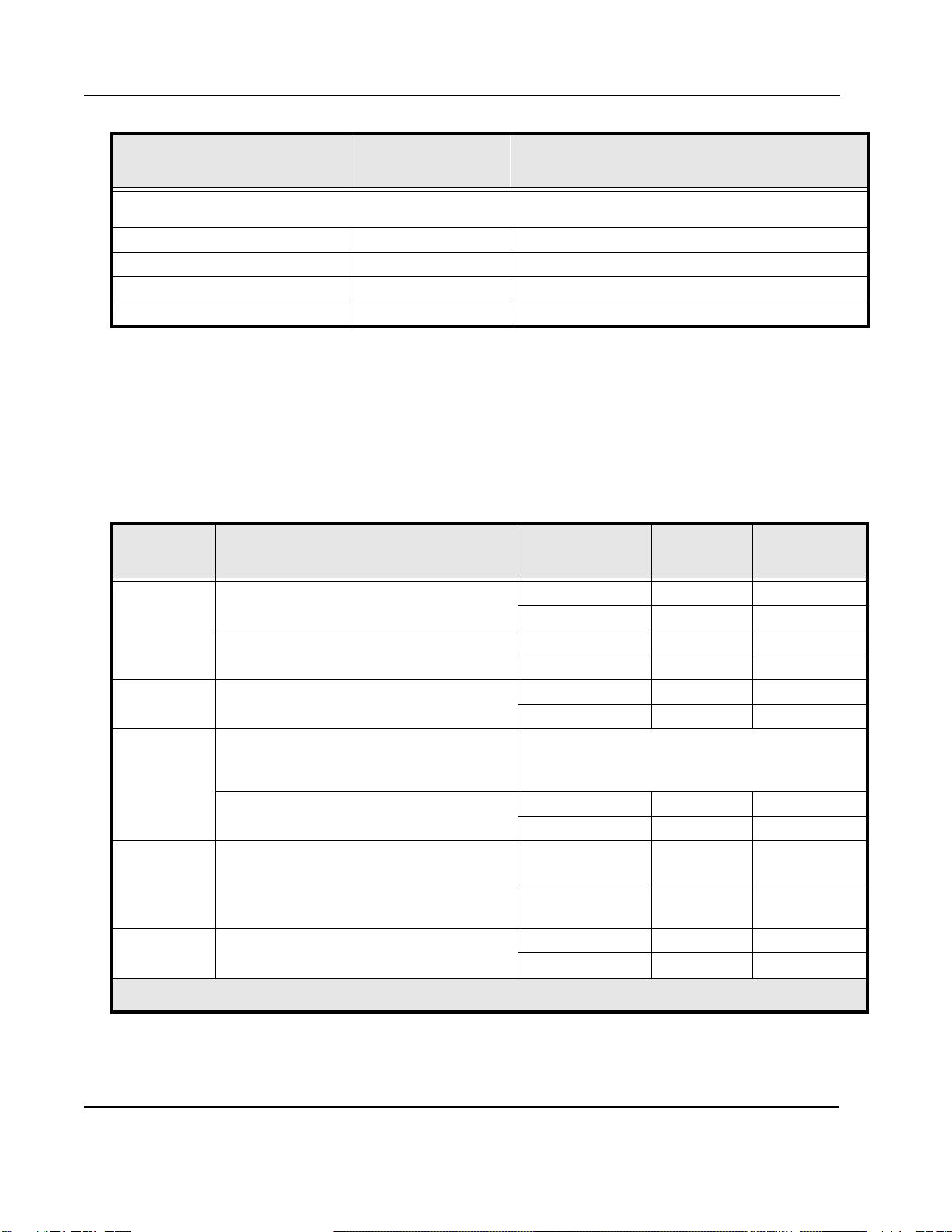
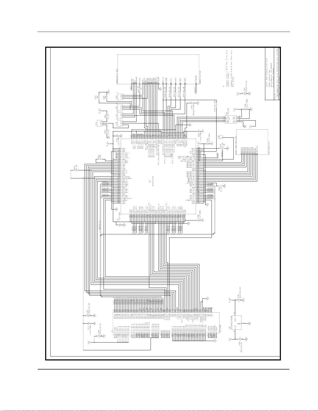
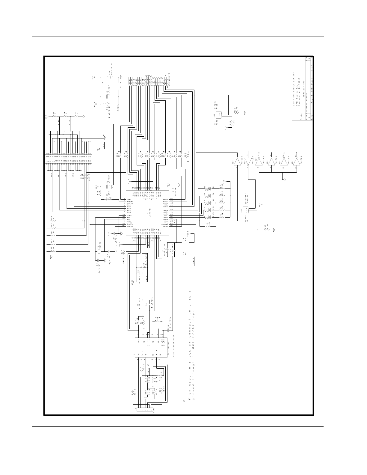
BILL OF MATERIALS AND BOARD SCHEMATICS
Table 7: LXD970 NIC Demo BOM
Item Qty Reference Description
1 16 C1, C2, C15, C16, C17, C29, C30, C31, C32,
C34, C35, C37, C38, C39, C41 .1µf/50V 10% 1206 SMD
2 5 C3, C4, C0, C42, C43 10µf/6.3V SMD
3 4 C5, C33, C40, C44 22µf/6.3V SMD TANT.CAP.EIA B
4 2 C6, C7 18pf/50 5% .0805
5 3 C8, C9, C10 .01µf/50V 10% .0805 SMD
61 C28 22µf/50V .0805 SMD
7 3 D1, D2, D5 Red LED DIFF
8 2 D3, D6 Green LED DIFF
9 1 D4 Yellow LED DIFF
10 7 JP2, JP3, JP4, JP5, JP6, JP7, JP8 3-pin Gold Straight Header
11 1 J2 RJ45 1 Position Jack Shielded PC Grade
12 1 J10 Miniature Test Point
13 2 L5, L6, L7, L8 Ferrite SMD Bead P9812
14 1 JP9 25-pin Dual Row Header
15 6 R1, R2, R3, R4, R5, R59 332Ω1% Metal SMD Resistor
16 8 R10, R11, R14, R15, R17, R18, R19, R20 49.9Ω1% Metal SMD Resistor
17 2 R12, R13 75Ω1% Metal SMD Resistor
18 2 R57, R16 100Ω1% Metal SMD Resistor
19 7 R21 R22, R23, R24, R25, R62, R63 4.75kΩ1% Metal SMD Resistor
20 18 R27, R28, R29, R31, R32, R33, R34, R35, R36,
R37, R38, R39, R40, R41, R54, R55, R60, R74 54.9Ω1% Metal SMD Resistor
21 1 R30 22kΩ1% Metal SMD Resistor
22 1 R56 2.43k 1% Metal SMD Resistor
23 8 R61, R64, R65, R66, R67, R68, R72, R73 10k 1% Metal SMD Resistor
24 3 R69, R70, R71 1k 1% Metal SMD Resistor
25 1 T1 10/100 MB Transformer
HALO TG22-S010ND
26 1 T1 10/100 MB Transformer
Pulse PE-68517
27 1 U1 LXT970A
28 1 U2 HEX inverter SMD SO-14 Package

8
29 1 U3 DEC 21143 LAN Controller
144-pin PQFP
30 1 U4 1k bit 5V EEPROM 8 DIP Pkg
31 1 U7 Surface Mount PLCC Pkg - 90ns
32 1 U8 3.3V Low Dropout Reg SOT-223 Pkg
33 1 Y1 25MHz Crystal HC49 Case
34 1 IC Socket for U7 32-pin Solder Trail PLCC Socket
35 1 IC Socket for U1 64-pin QFP Surface Mount IC Socket
36 1 IC Socket for U4 8-pin Solder Tail (Gold) DIP Socket
Table 7: LXD970 NIC Demo BOM – continued
Item Qty Reference Description

9
Figure 2: LXT970A NIC DEC 21143 Interface

10
Figure 3: LXT970A NIC LXT970AQC Interface

11
Figure 4: LXT970A NIC ROM Interface

EAST WEST ASIA/PACIFIC EUROPE
Eastern Area Headquarters &
Northeastern Regional Office Western Area
Headquarters Asia / Pacific Area
Headquarters European Area
Headquarters
234 Littleton Road, Unit 1A
Westford, MA 01886
USA
Tel: (978) 692-1193
Fax: (978) 692-1124
3375 Scott Blvd., #110
Santa Clara, CA 95054
USA
Tel: (408) 496-1950
Fax: (408) 496-1955
101 Thomson Road
United Square #08-01
Singapore 307591
Thailand
Tel: +65 353 6722
Fax: +65 353 6711
Parc Technopolis-Bat. Zeta 3,
avenue du Canada -
Z.A. de Courtaboeuf
Les Ulis Cedex 91974
France
Tel: +33 1 64 86 2828
Fax: +33 1 60 92 0608
North Central
Regional Office South Central
Regional Office Central Asia/Pacific
Regional Office Central and Southern
Europe Regional Office
One Pierce Place
Suite 500E
Itasca, IL 60143
USA
Tel: (630) 250-6044
Fax: (630) 250-6045
2340 E. Trinity Mills Road
Suite 306
Carrollton, TX 75006
USA
Tel: (972) 418-2956
Fax: (972) 418-2985
Suite 305, 4F-3, No. 75,
Hsin Tai Wu Road
Sec. 1, Hsi-Chih,
Taipei County, Taiwan
Tel: +886 22 698 2525
Fax: +886 22 698 3017
Feringastrasse 6
D-85774 Muenchen-
Unterfoerhring, Germany
Tel: +49 89 99 216 375
Fax: +49 89 99 216 319
Southeastern
Regional Office Southwestern
Regional Office Northern Asia/Pacific
Regional Office Northern Europe
Regional Office
4020 WestChase Blvd
Suite 100
Raleigh, NC 27607
USA
Tel: (919) 836-9798
Fax: (919) 836-9818
28202 Cabot Road
Suite 300
Laguna Niguel, CA 92677
USA
Tel: (949) 365-5655
Fax: (949) 365-5653
Nishi-Shinjuku, Mizuma
Building 8F
3-3-13, Nishi-Shinjuku,
Shinjuku-Ku
Tokyo, 160-0023 Japan
Tel: +81 3 3347-8630
Fax: +81 3 3347-8635
Torshamnsgatan 35
164/40 Kista/Stockholm,
Sweden
Tel: +46 8 750 3980
Fax: +46 8 750 3982
Latin/South
America
9750 Goethe Road
Sacramento, CA 95827
USA
Tel: (916) 855-5000
Fax: (916) 854-1102
Revision Date Status
1.4 01/99 Table 1 - Correct pins (37 and 38) in Nibble Mode and add pins (21 - 22, 31, 32) in Symbol Mode.
Globally change product part number from LXT970 to LXT970A.
1.3 12/97 Revise Note 6 of the software installation procedure and delete Note 7.
InternationalThe Americas
Corporate Headquarters
9750 Goethe Road
Sacramento, California 95827
Telephone: (916) 855-5000
Fax: (916) 854-1101
Web: www.level1.com
Copyright © 1998 Level One Communications, Inc. Specifications subject to change without notice.
All rights reserved. Printed in the United States of America.
UG-T970A-R1.4-0199
The products listed in this publication are covered by one or more of the following patents. Additional patents pending.
5,008,637; 5,028,888; 5,057,794; 5,059,924;5,068,628; 5,077,529; 5,084,866; 5,148,427; 5,153,875; 5,157,690; 5,159,291; 5,162,746; 5,166,635; 5,181,228;
5,204,880; 5,249,183; 5,257,286; 5,267,269; 5,267,746; 5,461,661; 5,493,243; 5,534,863; 5,574,726; 5,581,585; 5,608,341; 5,671,249; 5,666,129; 5,701,099
Table of contents
Other LevelOne Motherboard manuals