Zarlink Le51HE001V User manual

Le51HE001V
QLSLAC
Evaluation Board, Revision E User’s Guide
Rev. A, Ver. 2
October 2, 2007
Document Number: 080800

www.zarlink.com
Information relating to products and services furnished herein by Zarlink Semiconductor Inc. or its subsidiaries (collectively “Zarlink”) is believed to be reliable.
However, Zarlink assumes no liability for errors that may appear in this publication, or for liability otherwise arising from the application or use of any such
information, product or service or for any infringement of patents or other intellectual property rights owned by third parties which may result from such application or
use. Neither the supply of such information or purchase of product or service conveys any license, either express or implied, under patents or other intellectual
property rights owned by Zarlink or licensed from third parties by Zarlink, whatsoever. Purchasers of products are also hereby notified that the use of product in
certain ways or in combination with Zarlink, or non-Zarlink furnished goods or services may infringe patents or other intellectual property rights owned by Zarlink.
This publication is issued to provide information only and (unless agreed by Zarlink in writing) may not be used, applied or reproduced for any purpose nor form part
of any order or contract nor to be regarded as a representation relating to the products or services concerned. The products, their specifications, services and other
information appearing in this publication are subject to change by Zarlink without notice. No warranty or guarantee express or implied is made regarding the
capability, performance or suitability of any product or service. Information concerning possible methods of use is provided as a guide only and does not constitute
any guarantee that such methods of use will be satisfactory in a specific piece of equipment. It is the user’s responsibility to fully determine the performance and
suitability of any equipment using such information and to ensure that any publication or data used is up to date and has not been superseded. Manufacturing does
not necessarily include testing of all functions or parameters. These products are not suitable for use in any medical products whose failure to perform may result in
significant injury or death to the user. All products and materials are sold and services provided subject to Zarlink’s conditions of sale which are available on request.
Purchase of Zarlink’s I2C components conveys a license under the Philips I2C Patent rights to use these components in an I2C System, provided that the system
conforms to the I2C Standard Specification as defined by Philips.
Zarlink, ZL, the Zarlink Semiconductor logo and the Legerity logo and combinations thereof, VoiceEdge, VoicePort, SLAC, ISLIC, ISLAC and VoicePath are
trademarks of Zarlink Semiconductor Inc.
TECHNICAL DOCUMENTATION - NOT FOR RESALE
For more information about all Zarlink products
visit our Web Site at

Table of Contents i
Document ID# 080800 Date: Oct 2, 2007
Rev: AVersion: 2
Distribution: Public Document
TABLE OF CONTENTS
CHAPTER 1 INTRODUCTION . . . . . . . . . . . . . . . . . . . . . . . . . . . . . . . . . . . . . . . . . . . . . . . . . . . . . . . . . . . . . . 1
1.1 Overview . . . . . . . . . . . . . . . . . . . . . . . . . . . . . . . . . . . . . . . . . . . . . . . . . . . . . . . . . . . . . . . 1
1.2 Devices Supported and Board Options . . . . . . . . . . . . . . . . . . . . . . . . . . . . . . . . . . . . . . . . 1
CHAPTER 2 JUMPERS AND BOARD OPTIONS . . . . . . . . . . . . . . . . . . . . . . . . . . . . . . . . . . . . . . . . . . . . . . . 3
2.1 Device Selection Jumper Block . . . . . . . . . . . . . . . . . . . . . . . . . . . . . . . . . . . . . . . . . . . . . . 3
2.2 Jumper Blocks JM1 – JM4 . . . . . . . . . . . . . . . . . . . . . . . . . . . . . . . . . . . . . . . . . . . . . . . . . . 3
2.3 Jumper JM5 . . . . . . . . . . . . . . . . . . . . . . . . . . . . . . . . . . . . . . . . . . . . . . . . . . . . . . . . . . . . . 3
2.4 Jumpers JM6 – JM8 . . . . . . . . . . . . . . . . . . . . . . . . . . . . . . . . . . . . . . . . . . . . . . . . . . . . . . . 4
2.5 Jumpers JDVCC and JAVCC. . . . . . . . . . . . . . . . . . . . . . . . . . . . . . . . . . . . . . . . . . . . . . . . 4
2.6 Test Points . . . . . . . . . . . . . . . . . . . . . . . . . . . . . . . . . . . . . . . . . . . . . . . . . . . . . . . . . . . . . . 5
2.7 Breadboard Area . . . . . . . . . . . . . . . . . . . . . . . . . . . . . . . . . . . . . . . . . . . . . . . . . . . . . . . . . 5
CHAPTER 3 BOARD SETUP AND CONNECTIONS. . . . . . . . . . . . . . . . . . . . . . . . . . . . . . . . . . . . . . . . . . . . . 7
3.1 Overview . . . . . . . . . . . . . . . . . . . . . . . . . . . . . . . . . . . . . . . . . . . . . . . . . . . . . . . . . . . . . . . 7
3.2 Digital Interface . . . . . . . . . . . . . . . . . . . . . . . . . . . . . . . . . . . . . . . . . . . . . . . . . . . . . . . . . . 8
3.3 Power Connections . . . . . . . . . . . . . . . . . . . . . . . . . . . . . . . . . . . . . . . . . . . . . . . . . . . . . . . 9
3.4 Analog Interface and SLIC Device Control. . . . . . . . . . . . . . . . . . . . . . . . . . . . . . . . . . . . . . 9
3.5 Device Socket Orientation . . . . . . . . . . . . . . . . . . . . . . . . . . . . . . . . . . . . . . . . . . . . . . . . . 10
CHAPTER 4 SOFTWARE OPERATION . . . . . . . . . . . . . . . . . . . . . . . . . . . . . . . . . . . . . . . . . . . . . . . . . . . . . 11
4.1 Overview . . . . . . . . . . . . . . . . . . . . . . . . . . . . . . . . . . . . . . . . . . . . . . . . . . . . . . . . . . . . . . 11
4.2 WinSLAC2™ Software . . . . . . . . . . . . . . . . . . . . . . . . . . . . . . . . . . . . . . . . . . . . . . . . . . . . 11
CHAPTER 5 STAND-ALONE OPERATIONAL TEST PROCEDURES . . . . . . . . . . . . . . . . . . . . . . . . . . . . . . 13
5.1 Verifying Functionality of Channels . . . . . . . . . . . . . . . . . . . . . . . . . . . . . . . . . . . . . . . . . . 13
5.1.1 Channel Functionality Test Procedure . . . . . . . . . . . . . . . . . . . . . . . . . . . . . . . . . 13
5.2 Testing the AISN Path . . . . . . . . . . . . . . . . . . . . . . . . . . . . . . . . . . . . . . . . . . . . . . . . . . . . 15
5.3 Testing the AX, Z, and AR Paths . . . . . . . . . . . . . . . . . . . . . . . . . . . . . . . . . . . . . . . . . . . . 15
5.4 Testing the SLIC Device Control Lines . . . . . . . . . . . . . . . . . . . . . . . . . . . . . . . . . . . . . . . 16
CHAPTER 6 LE51HE001V EVALUATION BOARD SCHEMATIC AND BOM . . . . . . . . . . . . . . . . . . . . . . . . 17
6.1 Evaluation Board Schematic and BOM . . . . . . . . . . . . . . . . . . . . . . . . . . . . . . . . . . . . . . . 17
APPENDIX A GLOSSARY OF TERMS . . . . . . . . . . . . . . . . . . . . . . . . . . . . . . . . . . . . . . . . . . . . . . . . . . . . . . . 19

Le51HE001V Eval Board User Guide
ii
Zarlink Semiconductor Inc.
This page left intentionally blank.

CHAPTER
1
Zarlink Semiconductor Inc.
1INTRODUCTION
1.1 OVERVIEW
The Le51HE001V Evaluation Board, revision E, provides a platform to fully test and evaluate the
Zarlink Quad Low Voltage Subscriber Line Audio-Processing Circuit (QLSLAC) devices.
Programming and control of the QLSLAC device is fully supported via the accompanying VP-Script
or WinACIF software programs. In this document, all references to the SLIC Device Evaluation
Board refer to a Zarlink SLIC device.
1.2 DEVICES SUPPORTED AND BOARD OPTIONS
There are five types of QLSLAC device configurations: The Le58QL02/021/031 series and the
Le58QL061/063 series. These are nearly identical devices, except the Le58QL061/063 devices
contain a GCI interface option as well as the PCM/MPI interface. The Le58QL02/021/031 series
supports only the PCM/MPI interface.
Within each of the device series, there are different pin-out and package options. The current
design of the Le51HE001V evaluation board supports the 44-pin TQFP pin-outs for the Le58QL021
and the Le58QL061 QLSLAC devices.
Note:
The silk-screen of the evaluation board incorrectly states that the jumper positions for row B to row C will allow
the user to evaluate the Le58QL02 and Le58QL06 parts. These parts are not currently available in the TQFP
package option.
The following table displays which devices are supported by the evaluation board.
The layout for the Le51HE001V Evaluation Board (44-pin TQFP package) is shown in Figure 1–1.
Table 1–1 Supported QLSLAC Devices
QLSLAC Device Board OPN Supported Device Package
Le58Q021VC Le51HE001V 44-pin TQFP
Le58Q061VC Le51HE001V 44-pin TQFP

Le51HE001V Eval Board User Guide
2
Zarlink Semiconductor Inc.
Figure 1–1 Le51HE001V Evaluation Board Revision E Silk Screen

CHAPTER
3
Zarlink Semiconductor Inc.
2JUMPERS AND BOARD OP-
TIONS
2.1 DEVICE SELECTION JUMPER BLOCK
The 44-pin TQFP package evaluation board supports both the Le58QL021 and Le58QL061
QLSLAC devices. The pin-outs of both devices are identical when the being run in the PCM mode.
Therefore, the shunt blocks can be left in their default position on JR1 (i.e., row A shorted to row B).
When in the GCI mode, seven signal names for the Le58QL061 device change, but not their pin
assignment.
2.2 JUMPER BLOCKS JM1 – JM4
These jumpers are used to select different series capacitor values, or to select a direct DC
connection to the VOUT connector from the QLSLAC device’s analog output pins. Two capacitor
values (100 nF and 1.0 µF) are provided on the board. The table below shows the jumper
connection options.
The default position of the shunt, when shipped from the factory, and the pin numbering of the
jumper is shown in Figure 2–1:
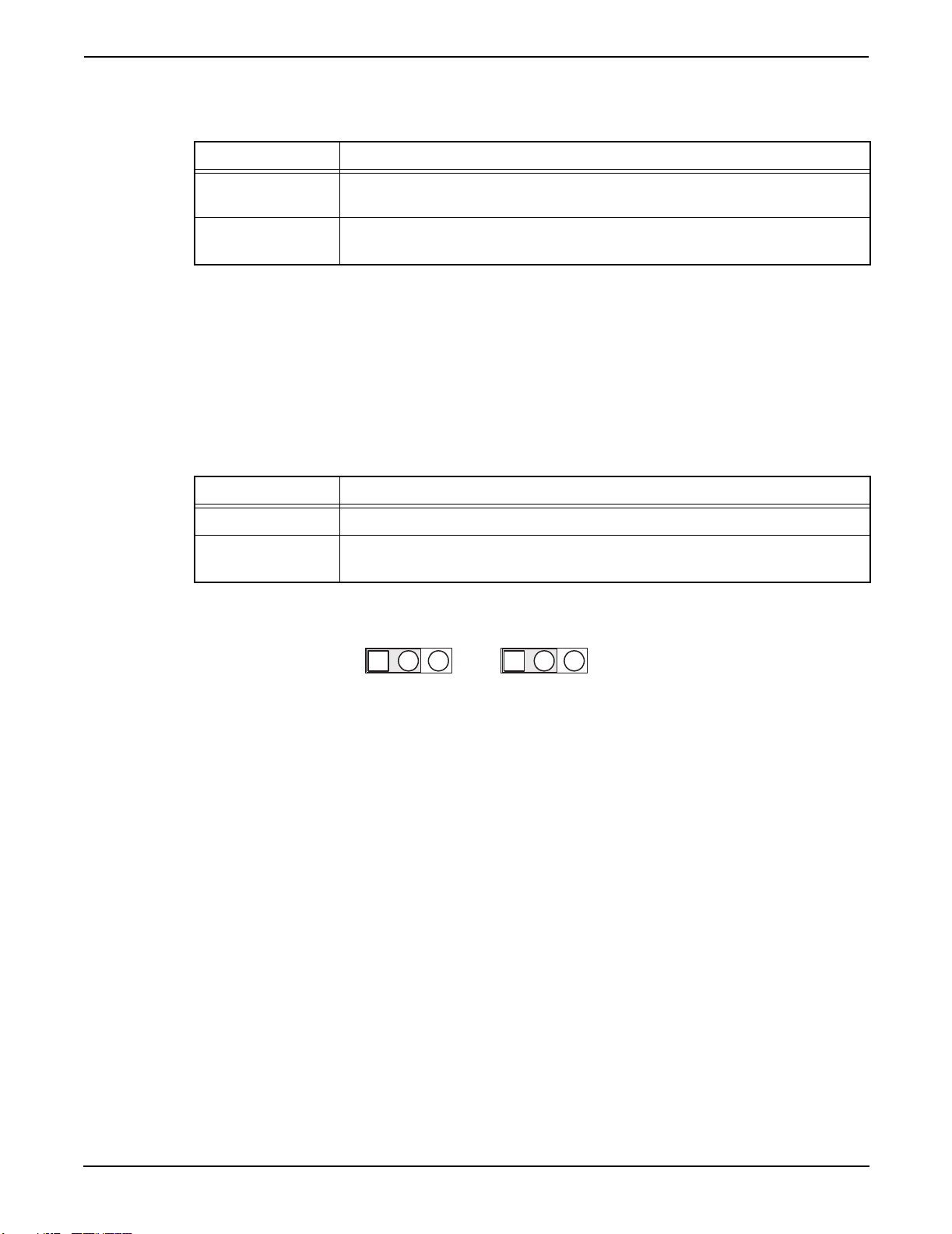
Figure 2–1 Jumper Blocks JM1 – JM4
2.3 JUMPER JM5
The QLSLAC device’s internal digital signal processor (DSP) operates from an internal master
clock. In the PCM/MPI mode, the master clock can be provided from the external MCLK input or the
device may internally derive the signal from the PCM (PCLK) clock input. In GCI mode the master
clock is derived from the DCL pin. If the internal clock is derived from PCLK, the MCLK/E1 pin can
be used as an E1 output to control Zarlnk SLIC devices having multiplexed switchhook and
ground-key detector outputs. Selection of the MCLK/E1 pin’s MCLK input or E1 output operation is
established by device programming. (Refer to Zarlink SLIC device data sheets and the QLSLAC
device data sheets for explanations and use of the E1 function.)
The JM5 jumper selects the board connection options to the QLSLAC device’s MCLK/E1 pin. When
this jumper is set for the E1 function, the MCLK/E1 pin of the QLSLAC device connects to the H1,
H2, H3, and H4 headers that supply the control input/output to an Zarlnk SLIC Device Evaluation
Board. When the jumper is set to the MCLK function, the MCLK/E1 pin connects to the MCLK signal
Table 2–1 JM1 – JM4 Jumper Connection Options
Output Pin Jumper Pin 1 to 6 Pin 2 to 5 Pin 3 to 4
VOUT1 JM1 DC 100 nF 1.0 µF
VOUT2 JM2 DC 100 nF 1.0 µF
VOUT3 JM3 DC 100 nF 1.0 µF
VOUT4 JM4 DC 100 nF 1.0 µF
1
2
34
5
6
Place shunt between pins 2 & 5 when
connecting to a Zarlink SLIC device.
Place shunt between pins 3 & 4 when
testing the board in a standalone mode.

Le51HE001V Eval Board User Guide
4
Zarlink Semiconductor Inc.
that originates from the VP Demo or the ACIF2-A Board through the IFB0 connector. The JM5
jumper settings are shown in the table below.
2.4 JUMPERS JM6 –JM8
Jumpers JM6 and JM7 connect the TSCB and TSCA signals respectively to pull-up resistors.
Jumper JM8 routes the INT signal to the LED indicator.
2.5 JUMPERS JDVCC AND JAVCC
Jumpers JDVCC and JAVCC select the supply voltage source for the QLSLAC device. JDVCC
supplies the DVCC input of the QLSLAC device and JAVCC supplies the AVCC input of the
QLSLAC device. The table below, and Figure 2–2 below, illustrate the jumper positions.
Figure 2–2 Jumpers JDVCC and JAVCC
As shown in Figure 2–2 above, shorting pin 1 to 2 selects the DVCC and AVCC supplies for the
QLSLAC device to be supplied via the SLAC_VCC connection.
The jumpers permit a single, clean point for monitoring device current consumption.
Table 2–2 JM5 Jumper Settings
Position Description
1-2 E1 signal connected to H1, H2, H3, and H4 headers for connection to a Zarlink
SLIC Device Evaluation Board.
2-3 External MCLK clock source routed to the MCLK/E1 pin of the QLSLAC device. The
standard factory setting is pin 2-3.
Table 2–3 JDVCC and JAVCC Jumper Settings
Position Description
1-2 Voltage is supplied via the SLAC_VCC connection (3.3 V nominal).
2-3 Voltage is supplied via the on-board regulator (VR1) (3.3 V regulated). Requires the
5V AUX_VCC to be supplied.
JDVCC
123
JAVCC
123

Le51HE001V Eval Board User Guide
5
Zarlink Semiconductor Inc.
2.6 TEST POINTS
Several test points are provided to facilitate signal checking when probing around the chip. The test
points and their descriptions are contained in the table below.
The first 12 (/RST-PCLK) are next to the IFB0 connector. VREF is to the right of the QLSLAC device
socket. VIN1 - VIN4 and VOUT1 - VOUT4 test points are located to the right of the QLSLAC device
socket between the control headers, H1 - H4 and the BNC connectors. Nine GND test points are
placed around the board (refer to Figure 1–1 on page 1-2).
2.7 BREADBOARD AREA
A breadboard area is provided on the board. This area may be used for adding any circuit
representative of the environment where the QLSLAC device may be used, and allows device
evaluation along with any such added circuit. The bread board area is located on the right hand
side of the board next to the BNC connectors. GND and VCC signals are provided to this area.
Each VIN and VOUT BNC has a trace connecting it to the adjacent row of pins in the breadboard
area. An example of this is shown in Figure 2–3 below.
Figure 2–3 VIN/VOUT BNC Trace
Table 2–4 PCM Test Points
PCM Test Point Description
/RST Reset input to the device. A logic Low will reset the QLSLAC device.
MCLK Master clock input by use for the digital signal processor.
DCLK The data clock input shifts data into and out of the microprocessor interface.
DRB The PCM Data Receive B port.
DIO Control data is serially written into or read from the QLSLAC device.
/INT The interrupt output pin. Active Low.
DXA The PCM Data Transmit A port.
/CS Chip Select (Active Low) enables the device for control data to/from the part.
DRA The PCM Data Receive A port.
DXB The PCM Data Transmit B port.
FS The Frame Sync input is an 8 kHz signal indetifying Time Slot/Clock Slot 0.
PCLK The PCM clock determines the rate at which PCM data is shifted.
VREF Analog Reference voltage output pin.
VIN1-VIN4,
VOUT1-VOUT4
Audio from the SLIC device.
Audio to the SLIC device.
GND There are 9 GND test points on the board.
VOUT4
VCC
GND
To JM4
VCC for the breadboard area is supplied by AUX_VCC.
The GND connection is the common GND for the board

Le51HE001V Eval Board User Guide
6
Zarlink Semiconductor Inc.
This page intentionally left blank.

CHAPTER
7
Zarlink Semiconductor Inc.
3BOARD SETUP AND CON-
NECTIONS
3.1 OVERVIEW
A representative connection of a complete Zarlink evaluation platform setup is shown in Figure 3-
1 and Figure 3-2. In both platforms, the host PC runs the software program appropriate to the type
of interface board. The interface board is connected to the host PC via a 9-pin cable connected to
the serial COM port (COM1 or COM2) of the PC. The Le51HE001V Evaluation Board connects
directly to the 50-pin connector of interface board. A SLIC Device Evaluation Board is connected to
the Le51HE001V Evaluation Board via a 20-pin ribbon cable and 2 BNC cables.
In Figure 3-1 the Le51HE001V Evaluation Board is connected to the VP Demo Board via the 50-
pin connector SPA. The host PC runs the VP-Script Software. The QLSLAC device is controlled
via the sub-menus of the software.
Figure 3–1 QLSLAC Device Evaluation Board Connection Diagram
In Figure 3-2 the Le51HE001V Evaluation Board is connected to the ACIF2-A board via the 50-pin
connector LNB#0. The host PC runs the WinACIF Software. The QLSLAC device is controlled via
the sub-menus of the software.
Figure 3–2 QLSLAC Device Evaluation Board Connection Diagram
Telephone
VP Demo
Board
QLSLAC SLIC
PCM-4
T1/E1
Analog
Telephone
ACIF2-A
QLSLAC SLIC
PCM-4
Digital
Analog

Le51HE001V Eval Board User Guide
8
Zarlink Semiconductor Inc.
A SLIC Device Evaluation Board is connected to one of the four available channels of the QLSLAC
device. The evaluation board has four pairs of BNC connectors, VIN1 - VIN4 and VOUT1 - VOUT4,
representing the analog inputs and outputs of the QLSLAC device's channels. These are connected
directly to the SLIC device's corresponding VTX and VRX BNC connectors. Control of the SLIC
device is provided via the digital control headers (H1 - H4). The 20-pin interconnect cable that is
provided with a Zarlink SLIC Device Evaluation Board can be plugged into any of the four headers
enabling quick and easy control of the SLIC device.
Test equipment can be connected to the tip/ring connectors of the SLIC Device Evaluation Board,
or it can be connected directly to the analog input/output of the evaluation board, bypassing the
SLIC device entirely. Digital PCM or T1/E1 access to test equipment is provided through either the
VP Demo Board or the ACIF2-A board.
3.2 DIGITAL INTERFACE
All PCM/MPI interface signals pass through IFB0, the 50-pin connector, from either the ACIF2-A
board or the VP Demo Board to the QLSLAC Device Evaluation Board. The Le58QL021 device
operates in a PCM data communication mode with a microprocessor control interface (PCM/MPI
mode). The Le58QL061 device is designed to operate in the PCM/MPI mode or in the General
Control Interface (GCI) mode. The table below lists the pin assignments for PCM and GCI modes.
When used in the GCI mode, some of these control signals have their functions redefined, as noted
by the shaded cells.
Table 3–1 Digital Interface Pin-Outs for PCM and GCI Modes
PCM Mode GCI Mode
Pin # Signal Pin # Signal Pin # Signal Pin # Signal
1 /RST 26 GND 1 /RST 26 GND
2 MCLK 27 GND 2 MCLK 27 GND
3 DCLK 28 GND 3 S0 28 GND
4 DRB 29 GND 4 DRB 29 GND
5DIO30GND 5S1 30 GND
6 /INT 31 GND 6 /INT 31 GND
7DXA32GND 7 DU 32 GND
8/CS33GND 8PG 33 GND
9DRA34GND 9 DD 34 GND
10 DXB 35 GND 10 DXB 35 GND
11 FS 36 GND 11 FSC 36 GND
12 PCLK 37 GND 12 DCL 37 GND
13-25 N/C 38-50 GND 13-25 N/C 38-50 GND

Le51HE001V Eval Board User Guide
9
Zarlink Semiconductor Inc.
3.3 POWER CONNECTIONS
Power for the board is supplied by three banana jacks, SLAC_VCC, GND and AUX_VCC. The
SLAC_VCC powers the QLSLAC device only. AUX_VCC powers the on-board voltage regulator,
VR1, pull-up resistors and the LED. Two jumpers allow for the power to be supplied from either
SLAC_VCC or AUX_VCC via the voltage regulator. Refer to "Jumpers JDVCC and JAVCC" on page
2-4 for more information.
3.4 ANALOG INTERFACE AND SLIC DEVICE CONTROL
The Analog Interface consists of the four pairs of analog transmit and receive BNC connectors and
are designed to be connected to the four-wire interface of the SLIC Device Evaluation Board. These
connector pairs are labeled VIN1 and VOUT1, VIN2 and VOUT2, VIN3 and VOUT3, and VIN4 and
VOUT4. The table below gives a short description of how the signals connect to each other.
Digital control of the SLIC Device Evaluation Board is provided through the H1, H2, H3, and H4
headers. These headers provide external (off board) control of the SLIC device, and monitor the
DETECT signal when the SLIC Device Evaluation Board has its own control select jumpers set to
the EXTERNAL control position. (Refer to the SLIC evaluation board documentation for more
information on control selection.) The table below lists the pin assignments of the SLIC device
control connectors.
Note:
The "x" denotes the specific channel (1–4) of the signal. The QLSLAC device generates the E1 signal when
so programmed. If the E1 signal is not generated by the QLSLAC device, the signal is pulled High.
Table 3–2 Power Supply Values
Input Voltage Minimum Typical Maximum
SLAC_VCC 3.13 V 3.3 V 3.47 V
AUX_VCC 3.4 V 5.0 V 20 V
Table 3–3 QLSLAC/SLIC Device Signal Connections
QLSLAC Device SLIC device Description
VOUTXVRX Decoupled output signal from QLSLAC to SLIC input
VINXVTX Output signal from SLIC to decoupled QLSLAC input
Table 3–4 SLIC Device Control Header Pin Assignments
Pin # Signal Pin # Signal
1CD2X2GND
3C3X4GND
5C4X6GND
7E18GND
9C5X10 GND
11 Pulled High 12 GND
13 CD1X14 GND
15 N/C 16 N/C
17 N/C 18 N/C
19 N/C 20 N/C

Le51HE001V Eval Board User Guide
10
Zarlink Semiconductor Inc.
3.5 DEVICE SOCKET ORIENTATION
The socket for the 44-pin TQFP QLSLAC device is oriented such that pin 1 of the device is towards
the right-hand side of the board near the bottom (refer to Figure 1–1 on page 1-2). The pin numbers
“11, 12, 22, 33, 34, and 44” are printed on the board around the corners of the device socket. These
numbers provide an easy reference for probing around the device.

CHAPTER
11
Zarlink Semiconductor Inc.
4SOFTWARE OPERATION
4.1 OVERVIEW
Two control platforms allow the user to communicate with the Le51HE001V Evaluation Board. The
first platform is the VP Demo Board and the VP-Script program or the Voice Path Mini-PBX
software. The second platform is the ACIF2-A Hardware Board along with its accompanying
WinACIF™ software program. A third software program, WinSLAC2™, is used to calculate the
required coefficients needed by the QLSLAC device.
4.2 WINSLAC2™ SOFTWARE
The WinSLAC software models the QLSLAC device, calculates programmable coefficients for
optimizing two-wire impedance, hybrid balance and transmit and receive responses. WinSLAC also
calculates and predicts transmission performance for:
• Two-wire Return Loss
• Four-wire Return Loss
• Transmit and Receive attenuation Distortion
• Transmit and Receive path equalization
• Two-wire Stability
For a more detailed description refer to the WinSLAC2 Software User's Guide, PID# 080779.
The VP Demo Board is one of the control platforms used for communicating with the evaluation
board in PCM/MPI mode. The VP-Script program uses a command menu to send information to
and receive information from the evaluation board.
Refer to the VP-Script Software User's Guide, PID# 080757 for more detailed information.
The ACIF2-A Hardware Board and the WinACIF Software are an alternate platform that can be
used to communicate with the chipset. Once the software has been initialized with the correct
chipset configuration, a command menu is used to send information to and receive information from
the QLSLAC device. The ACIF2-A Hardware Board supports both PCM and GCI modes.
Refer to the WinACIF Software User's Guide, PID# 080269 for more detailed information.

Le51HE001V Eval Board User Guide
12
Zarlink Semiconductor Inc.
This page intentionally left blank.

CHAPTER
13
Zarlink Semiconductor Inc.
5STAND-ALONE OPERA-
TIONAL TEST PROCEDURES
5.1 VERIFYING FUNCTIONALITY OF CHANNELS
This test will verify functionality of all four channels of the QLSLAC device. While somewhat lengthy
in setup, it will help the user to gain understanding of how the GX, GR, B, Z, R, X, AX, AR, and AISN
blocks work together. Refer to the QLSLAC device block diagram below.
Figure 5–1 QLSLAC Device Block Diagram
You will need the following equipment to perform this test:
• Appropriate platform board and accompanying software
• Le51HE001V Evaluation Board
• Dual Channel Oscilloscope
• Signal Generator
•BNCcables
• Banana Jack cables
5.1.1 Channel Functionality Test Procedure
Perform the following steps to verify the functionality of all four channels of the QLSLAC device:
1. Connect the evaluation board to the control platform (VP Demo or ACIF2-A Board).
2. Connect 5 V and GND to the ACIF board.
3. Connect the banana jacks of the Le51He001V to the supplies, and power up both boards.
4. On the PC, start the WinACIF program and select device.
5. Click OK on the message stating "Configuration Successful," then click on the QLSLAC Cmds
menu button.
Now, perform the following steps (or run the "initial.tcl" script on the Zarlink Application Tools and
Designs CD):
6. Click on the Hardware Reset button.
7. Click on the Pulse Reset Pin button.
8. Click on the Software Reset button.
9. Click on the Write Activate button. By default, all channels should be enabled. This can be ver-
ified by reading the "Wrt/Rd Enable Chan" register.
10. Set the Z and B filters to 0, as follows:
VIN DGIN AX
AISN
+AR
ADC
DAC Inter-
polator
Deci-
mator
+
Deci-
mator
Inter-
polator
ZB
+GX X LPF &
HPF
GR R LPF Ex-
pander TSA
TSA
Com-
pressor
High Pass Filter (HPF)
Full
Digital
Loopback
(FDL)
*
*
*
*
VOUT VREF
*
**
**
Lower Receive
Gain (LRG)
Cutoff Receive
Path (CRP)
TSA Loopback
(TLB)
Cutoff
Transmit
Path
(CTP)
Digital
TX
Digital
RX
1 kHz Tone
(TON)
0
* Programmable blocks

Le51HE001V Eval Board User Guide
14
Zarlink Semiconductor Inc.
a) Click on the Filter & Gains: Wrt/Rd B1 Filter Coefficients button. Input zero for each dec-
imal value on each channel.
b) Click on the Write button.
c) Click on the Filter & Gains: Wrt/Rd B2 Filter Coefficients button. Input zero for each dec-
imal value on each channel.
d) Click on the Write button.
e) Click on the Filter & Gains: Wrt/Rd Z (FIR & IIR) Filter Coefficients button. Input zero for
each decimal value on each channel.
f) Click on the Write button.
11. Set the GX and GR filters to unity gain and program/activate the X and R filters, as follows:
a) Click on the Wrt/Rd GX Filter Coefficients button.
b) Enter "Gain = 1: 01 90".
c) Click on the Write button.
d) Click on the Wrt/Rd GR Filter Coefficients button.
e) Enter "Gain = 1: 01 11".
f) Click on the Write Coeff button.
g) Click on the Wrt/Rd X Filter... button.
h) Enter "1" for the decimal value on each channel.
i) Click on the Write button.
j) Click on the Wrt/Rd R Filter... button.
k) Enter "1" for the decimal value on each channel.
l) Click on the Write button.
12. Set AX/AR/AISN, as follows:
a) Click on the Wrt/Rd AISN & Analog Gains button.
b) Ensure AX, AR and DGIN are set to 0.0 dB.
c) Ensure the Analog Impedance Scaling Network Gain: window displays "Cut-off."
d) Click on the Write button.
13. Set the operating function bits, as follows:
a) Click on the Wrt/Rd Operating Functions button.
b) Set Gr, Gx, X, R, Z and B to "1" to enable the programmed filter values.
c) Click on the Write button.
14. When you see the Main Menu screen, click on the ACIF board menu, then click the PCM-4
Interface button.
15. Set the DXA and DRA connection path to match the diagram shown in Figure 5–2 below.
Figure 5–2 Routing DXA to DRA via the PCM Menu

Le51HE001V Eval Board User Guide
15
Zarlink Semiconductor Inc.
5.2 TESTING THE AISN PATH
The first path is via the AISN gain block. This test will allowing the user to see how AISN can affect
a signal by simply changing the AISN Gain value and writing that value to the QLSLAC device.
Once again, you can either load the script, "aisn_path.tcl" or follow the procedures.
To test the AISN function, do the following:
• Input a 1VPP
, 1 kHz sine wave to VIN1 of channel 1, and connect an oscilloscope to the
VOUT1 BNC.
– Click on Wrt/Rd AISN & Analog Gains button.
– Click on +0.6250 and press Write.
– The signal should jump to approximately 568 mVRMS.
– Click on -0.625 and press Write.
– The signal will drop to approximately 131m mVRMS.
The signal is now looped through the AISN block in the QLSLAC device. Selecting any of the values
in the AISN Gain screen will immediately affect the signal.
Note:
Before continuing to the next test, set the AISN Gain block back to cut-off.
5.3 TESTING THE AX, Z, AND AR PATHS
The second test path is via the AX, Z, and AR blocks only. This test causes the 1 kHz signal, input
to channel 1, to be looped through a specific path, and output to the VOUT1 BNC. Independently
changing the AX, AR, and Z Gain values and writing that value(s) to the QLSLAC will affect the
output signal, therefore allowing the user to see how these blocks can affect a signal. Either run
the "ax_z_ar_path.tcl" script or perform the steps below.
1. Click on the Wrt/Rd Operating Functions button, then do as follows:
a) Enable Z filter by setting it to a "1".
b) Write Operating Functions.
2. Click on the Wrt/Rd Z filter (FIR & IIR) button, then enter "1" for the decimal value of each chan-
nel to activate the Z filter.
Connect an external 1 kHz supplied by a signal generator:
• Once the Z filter is enabled the signal will become 0.345 mVRMS.
• To have a better understanding how the AX and AR filters affect the signal, open the AISN
Programming menu and change the AX or AR from a "0" to a "1". (Do not change AX and AR
simultaneously as this will have no visible effect on the signal since AX provides a +6.02 dB
gain and AR attenuates by a 6.02 dB gain.)
• If setting AX = 1 (AR = 0), the signal becomes a 0.690 mVRMS.
• If setting AR = 1 (AX = 0), the signal becomes a 0.172 mVRMS.
When using a DVM for measuring the peak-to-peak AC signal, from a generator, the DVM will
always display the Root Means Square (RMS) value. An oscilloscope is designed to display the
VPP value, as well as the shape, of the signal. To convert from VPP to RMS refer to the formula
below.
RMS TRUE
2.828
----------------------=

Le51HE001V Eval Board User Guide
16
Zarlink Semiconductor Inc.
5.4 TESTING THE SLIC DEVICE CONTROL LINES
This procedure will test the Control and Data (inputs/outputs), CD1 and CD2, and the three SLIC
device control lines (C3, C4, C5) of the QLSLAC device. To accomplish this you will need two 20-
pin cables to connect H1 to H2 and H3 to H4.
Perform the following steps to test the SLIC device control lines:
1. Set the Wrt/Rd Enable Channel Register buttons so that only channels 1 and 3 are selected.
2. From the QLSLAC Cmds menu, click once on the IO Direction & Read Status button, then do
as follows:
a) Change IOD1, IOD2, IOD3, IOD4, and IOD5 to a "1".
b) Click on the Wrt Input Output Register Direction button.
3. Click on the Wrt/Rd SLIC IO Direction menu option, and do as follows:
a) Change CD1, CD2, C3, C4, and C5 to a "1".
b) Click on the Wrt Input/Output Register button.
4. From the Wrt/Rd Enable Channel Register menu, do as follows:
a) Disable channels 1 and 3.
b) Enable channels 2 and 4.
5. From the Wrt/Rd SLIC IO Direction menu, do as follows:
a) Leave IOD1 through IOD5 set to "0".
b) Click on the Write button.
6. From the Wrt/Rd Enable Channel Register menu, do as follows:
a) Disable channel 4.
b) Enable channel 2.
c) Click on the Rd/CLR Real Time Data Register option. You will see the data pattern output
by channel 1.
d) Disable channel 2.
e) Enable channel 4.
f) Click on the Rd/CLR Real Time Data Register option for channel 4. You will see the data
pattern output by channel 3
Please remember that the control signals are mapped to the H1-H4 headers in the following
manner:
Table 5–1 CD1x –C5x Control Signal Mapping to H1 –H4 Headers
Control Signal Mapping Description
CD1x Routed to pin 13 of header to monitor the status of DET
CD2x Routed to pin 1 of header Hx as C1 bit for the SLIC device
C3x Routed to pin 3 of header Hx as C2 bit for the SLIC device
C4x Routed to pin 5 of header Hx as C3 bit for the SLIC device
C5x Routed to pin 9 of header Hx as C5 bit of the SLIC device
Table of contents
Other Zarlink Motherboard manuals