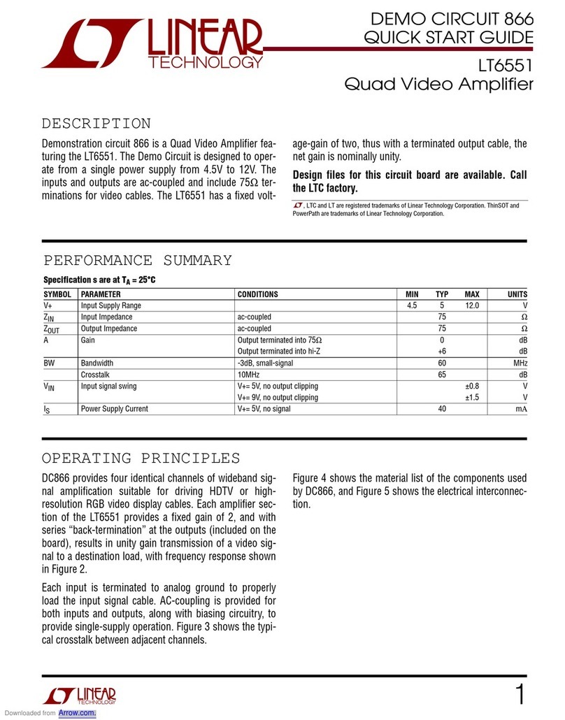
DESCRIPTION
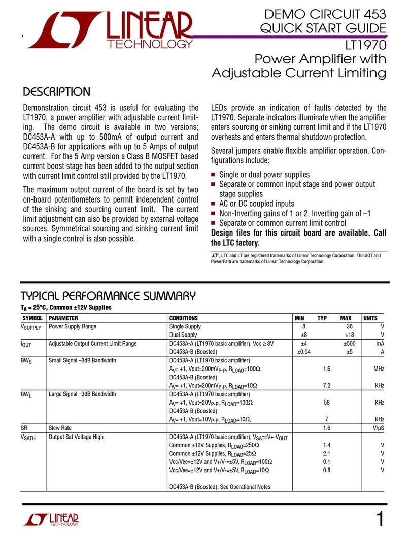
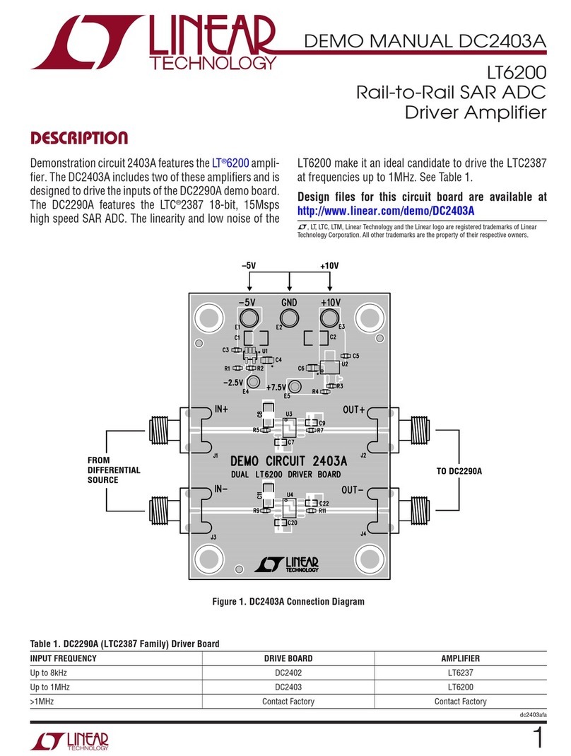
Demonstration circuit 1363 is a General Purpose High-
Side Current-Sense Amplifier featuring the LT61 7.
This demo board amplifies an on-board current-sense
resistor voltage-drop, providing a precision uni-polar
output voltage proportional to load current. The demo
circuit includes scaling resistors that program the gain of
the circuit to 5 V/V. The LT61 7 is pow ered from the
same supply that the sense resistor is connected to and
provides a ground referenced output. The LT61 7 can
perform current measurements on supplies ranging from
2.7V to 36V. Since the output voltage is developed as a
controlled current through a load resistance, ground-
loop errors can be eliminated by simply locating the load
resistor at the destination point (subsequent signal
processing such as A/D conversion). Remote loading can
be evaluated by simply removing the on board load
resistor (R3).
DC1363 is fabricated from FR-4 6 high-temp epoxy-
glass so that the full 15 ° operation of the LT61 7 can
be demonstrated. Other key performance characteristics
of the LT61 7 and DC1363 are show n in the
Performance Summary below .
Design files for this circuit board are available. Call
the LTC factory.
L
, LT are registered trademarks of Linear Technology Corporation. Other product names
may be trademarks of the companies that manufacture the products.
PERF ORM ANCE SU M M ARY
Specifications are at T
A
= 25°C
SY BOL PARA ETER CONDITIONS IN TYP AX UNITS
V
IN
M onitored Supply Input Range
2.7 3… 28 36
V
M O N
M easurement Output Signal I
OUT
= 5A
2.5
I
M ON
M easurement Output Signal (current mode) I
OUT
= 5A, R3 removed
5
I
OUT
Output Load Current Range Thermal limit of R
SENSE
5
I
INQ
V
IN
Quiescent Current V
IN
=12V, I
OUT
= A
65
t
R
V
M ON
step-response time I
OUT
step from A to 5A 5 µs
OPERATING PRINCIPL ES
The LT61 7 operates by amplifying the voltage drop on a
sense resistor placed in series w ith the pow er source of a
load to be monitored. The sense inputs of the amplifier
differentially measure the sense-resistor drop to control
an internal variable current source that allow s translation
of the input information to a level referenced to V–
(ground in this demo circuit). The circuit gain is
established by the ratio of the output resistor to the input
resistor and is essentially as accurate as the resistors
used. In DC1363 as shipped, the sense resistor installed
is 1 m
Ω
and the resistor ratio sets the gain to 5 V/V, so
the nominal output scaling is 5 mV per Ampere of load
current. O ther scalings can be produced by resistor
replacement on the demo circuit.
The DC1363 Schematic diagram is show n in Figure 2.
H ig h Te m p e ra t re H ig h S id e
C rre n t S e n se in a S OT-


