1
dc1984af
DEMO MANUAL DC1984A
Description
LTC5510
1MHz to 6GHz Wideband
High Linearity Active Mixer
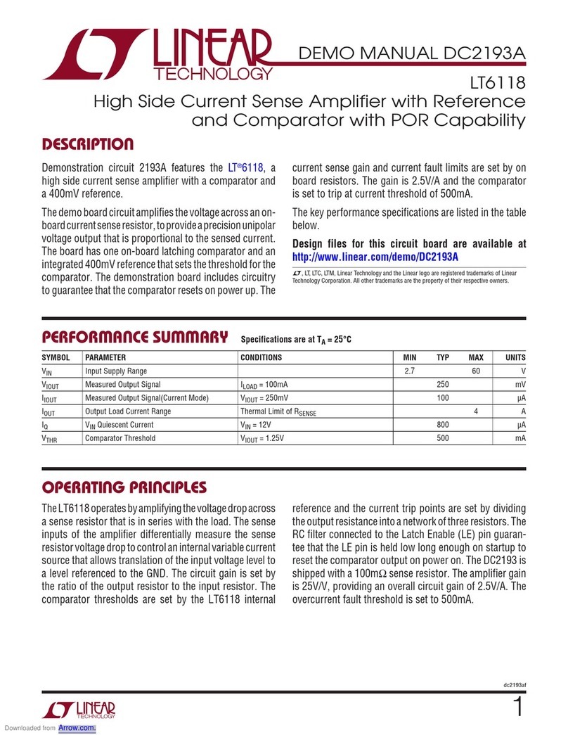
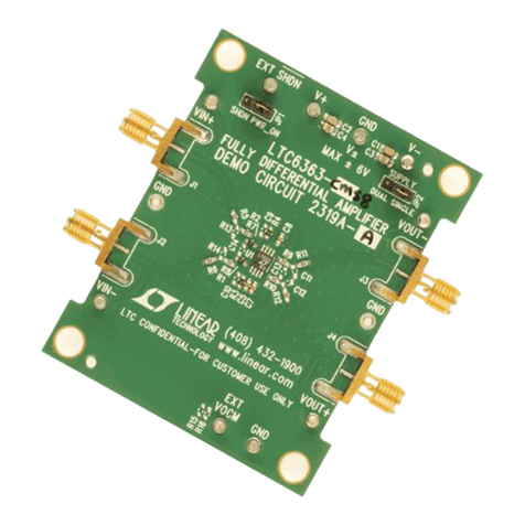
Demonstration circuit 1984A showcases the LT C
®
5510.
wideband high linearity active mixer for VHF/UHF upmixer
applications, where a 70MHz input signal is upconverted
to the 100MHz to 1GHz output range. Its input port is
optimized for 30MHz to 2.6GHz, and its output port is
optimized for 10MHz to 1.3GHz. The LO input can be
either high side or low side.
Another demonstration circuit, the DC1983A, utilizing a
multilayer chip hybrid balun, is designed for evaluating
the LTC5510 for wideband up/downmixer applications
with 30MHz to 3GHz input and 1.2GHz to 2.1GHz output.
DEMO BOARD INPUT RANGE LO RANGE OUTPUT RANGE
DC1983A 30MHz to 3GHz 5MHz to 6GHz 1.2GHz to 2.1GHz
DC1984A 30MHz to 2.6GHz 5MHz to 6GHz 10MHz to 1.3GHz L, LT, LTC, LTM, Linear Technology and the Linear logo are registered trademarks of Linear
Technology Corporation. All other trademarks are the property of their respective owners.
performance summary
The LTC5510 is a high linearity active mixer optimized
for applications requiring very wide input bandwidth,
low distortion and low LO leakage. The IC includes a
double-balanced active mixer with an input buffer and a
high speed LO amplifier. The mixer can be used for both
up- and down-conversion and requires only 0dBm of LO
power to achieve excellent distortion and noise perfor-
mance. The LTC5510 is optimized for 5V, but can also
be used with a 3.3V supply with reduced performance.
The shutdown function allows the part to be disabled for
further power saving.
Design files for this circuit board are available at
http://www.linear.com/demo/DC1984A
PARAMETER CONDITIONS VALUE UNITS
Input Frequency Range 30 to 2600 MHz
Output Frequency Range 10 to 1300 MHz
LO Input Frequency Range 5 to 6000 MHz
LO Input Power Range –6 to 6 dBm
Supply Voltage Range 5V Supply, R1 = Open (Default Configuration)
3.3V Supply, R1 = 2kΩ
4.5 to 5.3
3.1 to 3.5
V
V
Supply Current 5V Supply, R1 = Open (Default Configuration)
3.3V Supply, R1 = 2kΩ
98
90
mA
mA
Total Supply Current During Shutdown EN = Low 1.3 mA
EN Input High Voltage (On) >1.8 V
EN Input Low Voltage (Off) <0.5 V
EN Input Current –0.3V to VCC + 0.3V –20 to 200 µA
Turn-On Time EN: Low to High 0.6 µs
Turn-Off Time EN: High to Low 0.6 µs
Temperature Monitor Pin (TEMP)
DC Voltage at TJ= 25°C
IIN = 10µA
IIN = 80µA
697
755
mV
mV
Temperature Monitor Pin (TEMP)
Voltage Temperature Coefficient
IIN = 10µA
IIN = 80µA
–1.80
–1.61
mV/°C
mV/°C
Specifications are at TC= 25°C, VCC = 5V, EN = High, PLO = 0dBm,
PIN = –10dBm (–10dBm/tone for two-tone tests), unless otherwise noted. (Note 1)
