Linear LTC4316 Quick setup guide

1
dc2217af
DEMO MANUAL DC2217A
Description
LTC4316
Single I2C/SMBus
Address Translator
Demonstration circuit 2217A features the LT C
®
4316 single
I2C/SMBus address translator. The LTC4316 enables one
or more I2C or SMBus slave devices to translate their
hardwired address to a different address. This allows
slaves with the same address to coexist on the same
bus. Only discrete resistors are needed to select the new
address and no software programming is required. Up to
127 different translations are available.
The LTC4316 has a rich set of features including:
nAllowing Multiple Slaves with the Same Address to
Coexist on the Same Bus.
nResistor Configurable Address Translating
nCompatibility with SMBus, I2C and I2C Fast Mode
nPass-Through Mode for General Call Addressing
nLevel Translation for 2.5V, 3.3V, and 5V Buses
nStuck Bus Timeout
nPrevention of SDA and SCL Corruption During Live
Board Insertion and Removal
L, LT, LTC, LTM, Linear Technology and the Linear logo are registered trademarks and Hot
Swap and QuikEval are trademarks of Linear Technology Corporation. All other trademarks are
the property of their respective owners.
nSupport for Bus Hot Swap™
n10-Lead MSOP or DFN 3mm × 3mm Package
The LTC4316 incorporates a pass-through mode which
disables the address translating and allows general call
addressing by the master. The LTC4316 is designed to
automatically recover from abnormal bus conditions like
bus stuck low or premature stop bits. There are three LT C
parts in this family with different numbers of inputs and
outputs. The part numbers are as follows:
PART NUMBER NUMBER OF INPUT
CHANNELS
NUMBER OF OUTPUT
CHANNELS
LTC4316 1 1
LTC4317 1 2
LTC4318 2 2
DC2217Ademonstratesonlythe LTC4316. The otherparts
provide similar functions with differences listed in their
respective data sheets.
Design files for this circuit board are available at
http://www.linear.com/demo/DC2217A

2
dc2217af
DEMO MANUAL DC2217A
Quick start proceDure

3
dc2217af
DEMO MANUAL DC2217A
Quick start proceDure
OVERVIEW
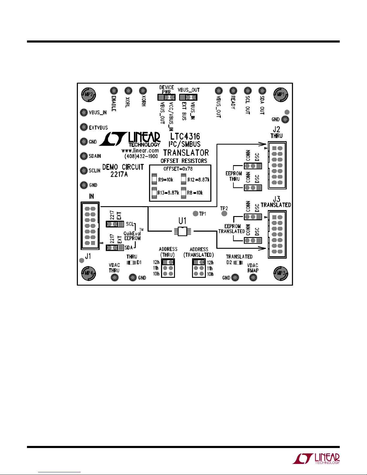
The DC2217A is designed to demonstrate the ability of
the LTC4316 to offset an incoming I2C address field on
the SDAIN pin to any other I2C address on the SDAOUT
pin. The I2C data input to the card is generated from the
DC590 in conjunction with a PC.
ThisisimplementedbyEXCLUSIVE ORingtheinput address
with a fixed offset that is determined by resistors R8, R9,
R12, and R13, located on the OFFSET RESISTORS section
on the top center of the board. These resistor values are
selected by using values shown in Table 3 and Table 4 of
the LTC4316 data sheet.
Input I2C serial data (SDAIN) and serial clock (SCLIN) are
applied to the DC2217A via a connecting cable between a
DC590 USB SERIAL CONTROLLER and IN jack J1 of the
DC2217A. These incomingsignalsare connectedto SCLIN
and SDAIN of the LTC4316 (U1), as well as to the SCL
and SDA pins of U2, an LTC2631 DAC. Another LTC2631
DAC, U3, has its SCL and SDA connected to SDAOUT
and SCLOUT of the LTC4316 TRANSLATOR. Both DACs
can be programmed to one of three addresses by use of
their CA0 inputs. These addresses are selected by jumper
pins ADDRESS (THRU) and ADDRESS (TRANSLATED).
For the purposes of testing the board, both are selected
to respond to address 0x12h.
If both DACs were connected to SDAIN and SCLIN, they
would both respond at the same time when address 0x12h
is received. However, since DAC U3 is connected to SD-
AOUT and SCLOUT of U1, and U1 is set for a 0x78h offset
by the OFFSET RESISTORS, it will respond to the address
0x6Ah. The data bits are set to full-scale for the DACs.
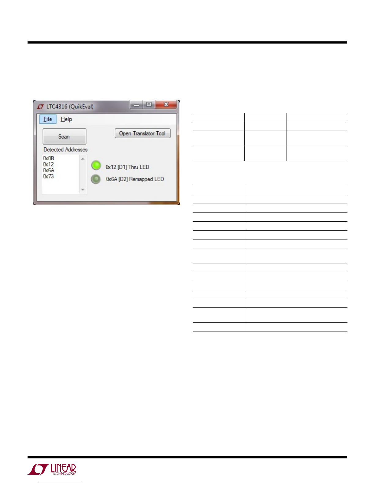
The net result is that when address field 0x12h is sent
from the DC590 with data bits set to full-scale, the LED
designated THRU will be illuminated. When address field
0x6Ah is sent, the LED designated TRANSLATED will be
illuminated. This shows that an address translation has
occurred because of the offset programmed into address
translator U1, the LTC4316.
Jumper options VBUS_OUT and DEVICE POWER allow
operation ofthe LTC4316 at different VCC and I2Cbus levels
than the 5V supplied from the DC590. With VBUS_OUT
in the VBUS_IN position, and DEVICE PWR in the VCC/
VBUS_IN position, all power for VCC of U1 and SCLIN,
SDAIN, SCLOUT, and SDAOUT bus pull-up voltages will
be sourced by the DC590. With EXT BUS selected by the
VBUS_OUT jumper and VCC/VBUS_IN selected by the
DEVICE PWR jumper, VCC of U1 will be sourced by the
5V from the DC590 along with SCLIN, SDAIN bus pull up
resistors while SCLOUT and SDAOUT will be sourced from
the EXTVBUS turret. With VBUS_OUT jumper in the EXT
BUS position and DEVICE PWR in the VBUS_OUT posi-
tion, VCC for U1 as well as SCLOUT and SDAOUT will be
sourced from the EXTVBUS turret. This gives maximum
flexibility of input and output I2C bus levels for use with
external bus structures.
Optional connections allow selection and control of other
QuikEval™ demonstration circuits using the THRU and
TRANSLATED connectors. The EESCL and EESDA lines
from J1 may be configured to address either the onboard
EEPROM U4, or EEPROMs located on other QuikEval
demonstration circuits by using the QuikEval EEPROM
SCL and SDA jumpers. For normal operation, the SCL and
SDA jumpers should be in the 2217 position.

4
dc2217af
DEMO MANUAL DC2217A
PROCEDURE
Connect the DC2217A and DC590 as shown in Figure 1.
Insert the USB cable into a USB port on the PC.
Quick start proceDure
Figure 1. Connection of DC2217A to DC590
QuikEval Interface
The DC2217A can be connected to a DC590 and used
with QuikEval software. The DC590 connects to a PC
through USB. QuikEval automatically detects the demo

5
dc2217af
DEMO MANUAL DC2217A
Quick start proceDure
Figure 2. Evaluation Software Interface
board and brings up the LTC4316 Evaluation Software
Interface (Figure 2). The QuikEval software is available at:
http://www.linear.com/QuikEval
Interface Design
The QuikEval interface consists of a Scan button which,
when pressed, causes the software to poll every I2C ad-
dress one at a time and listen for an acknowledge. Every
address that acknowledges is then listed in the Detected
Address list box directly beneath the Scan button. Once
the addresses are detected, the software determines
which ones correspond to the LEDs on the demo board.
At this point, clicking on the DAC Thru or DAC Translated
light-up control will cause the corresponding LED on the
demo board to illuminate. The Open Translator Tool but-
ton opens a tool that allows users to design an I2C bus
using LTC4316 I2C devices in an easy to use graphical
format. Figure 2 shows the results of selecting the Scan
button on a DC22117A with a standard configuration.
The Detected addresses show the All Call address, the
address of the DAC on the incoming I2C bus, the address
of the translated output I2C bus, and the address of the
on board EEPROM. The 0x12 [D1] Thru LED button has
been selected and corresponds to the THRU LED on the
DC2217A being illuminated.
Table 1. Input and Output Connections
NOMENCLATURE CONNECTOR DESCRIPTION
IN J1 Connection to DC590
THRU J2 Optional Output for
Customer Use
TRANSLATED J3 Optional Output for
Customer Use
Table 2. Turrets
NOMENCLATURE DESCRIPTION
VDAC THRU Analog Output of Thru Address DAC U2
VDAC RMAP Analog Output of Translated Address DAC U3
GND Ground
SCL OUT Serial Clock on Output Side of U1
SDA OUT Serial Data on Output Side of U1
READY READY Pin of U1
VBUS_OUT VCC Bus Voltage Selected by VBUS_OUT
Jumper for SCLOUT and SDAOUT
SCL IN U1 SCLIN Pin
SDAIN U1 SDAIN Pin
XORL U1 XORL Pin
XORH U1 XORH Pin
ENABLE U1 ENABLE Pin
EXTVBUS Input for External VCC for U1 and Input Pull
Up Supply
VBUS_IN Internal VCC Bus Supplied by DC590

6
dc2217af
DEMO MANUAL DC2217A
Quick start proceDure
Table 3. Jumpers
NOMENCLATURE DESCRIPTION DEFAULT POSITION
ADDRESS (THRU) Selects Address of
D/A U2
12h
ADDRESS (Translated) Selects Address of
D/A U3
12h
QuikEval EEPROM SCL Selects SCL Source of
EEPROM
2217
QuikEval EEPROM SDA Selects SDA Source of
EEPROM
2217
EEPROM THRU Optional EEPROM J2
Select
Optional
EEPROM THRU Optional EEPROM J2
Select
Optional
EEPROM TRANSLATED Optional EEPROM J3
Select
Optional
EEPROM TRANSLATED Optional EEPROM J3
Select
Optional
DEVICE PWR Selects Power Source
of VCC from Either
DC590 or VBUS_OUT
VCC/VBUS_IN
VBUS_OUT Selects VBUS_OUT
from Either DC590
or External Power
Source (EXTVBUS)
VBUS_IN
Table 4. LEDs
NOMENCLATURE LED DESCRIPTION
THRU (Green) D1 Illuminates When DAC U2 is
Addressed and Data FF is Received
TRANSLATED (Green) D2 Illuminates When DAC U3 is
Addressed and Data FF is Received

7
dc2217af
DEMO MANUAL DC2217A
Information furnished by Linear Technology Corporation is believed to be accurate and reliable.
However, no responsibility is assumed for its use. Linear Technology Corporation makes no representa-
tion that the interconnection of its circuits as described herein will not infringe on existing patent rights.
schematic Diagram
5
5
4
4
3
3
2
2
1
1
D D
C C
B B
A A
GND
SDAIN
SCLIN
GND
XORH
VBUS_IN
XORL
ENABLE
EXTVBUS
VBUS_OUT
READY
SCL OUT
SDA OUT
GND
VBUS_OUT
EXT BUS
VBUS_IN
VBUS_OUT
VCC/VBUS_IN
DEVICE
PWR
VCC
VBUS_OUT
SDAOUT
SCLOUT
SCLIN
SDAIN
DATE:
IC NO.
SHEET OF
TITLE: DEMO CIRCUIT SCHEMATIC,
APPROVALS
PCB DES.
APP ENG.
Fax: (408)434-0507
Milpitas, CA 95035
Phone: (408)432-1900
1630 McCarthy Blvd.
LTC Confidential-For Customer Use Only
CUSTOMER NOTICE
LINEAR TECHNOLOGY HAS MADE A BEST EFFORT TO DESIGN A
CIRCUIT THAT MEETS CUSTOMER-SUPPLIED SPECIFICATIONS;
HOWEVER, IT REMAINS THE CUSTOMER'S RESPONSIBILITY TO
VERIFY PROPER AND RELIABLE OPERATION IN THE ACTUAL
APPLICATION. COMPONENT SUBSTITUTION AND PRINTED
CIRCUIT BOARD LAYOUT MAY SIGNIFICANTLY AFFECT CIRCUIT
PERFORMANCE OR RELIABILITY. CONTACT LINEAR
TECHNOLOGY APPLICATIONS ENGINEERING FOR ASSISTANCE.
THIS CIRCUIT IS PROPRIETARY TO LINEAR TECHNOLOGY AND
SUPPLIED FOR USE WITH LINEAR TECHNOLOGY PARTS. SCALE = NONE
www.linear.com
SIZE:
SKU NO. SCHEMATIC NO. AND REVISION:
12
N/A
M.HAWKINS
BOB SMITH
LTC4316
I²C / SMBUS TRANSLATOR
DC2217A 710-DC2217A_REV02
Friday, June 05, 2015
E5
E18
R9
10k
1206
E17
C4
0.1uF
LTC4316
U1
SCLIN
10
GND
1
ENABLE
5
XORL
3
XORH
2
READY
6
SDAIN
7
SDAOUT
8
SCLOUT
9
VCC
4
E6
R6
10k
E9
JP9
1
3
2
E13
R15
10k R7
10k
E7
E12
E15
E14
R12
8.87k
1206
JP10
1
3
2
R13
8.87k
1206
R10
10k
E10
E11 R14
10k
E8
R11
10k
E16
R8
10k
1206

8
dc2217af
DEMO MANUAL DC2217A
Linear Technology Corporation
1630 McCarthy Blvd., Milpitas, CA 95035-7417
(408) 432-1900 ●FAX: (408) 434-0507 ●www.linear.com
© LINEAR TECHNOLOGY CORPORATION 2015
LT 0915 • PRINTED IN USA
DEMONSTRATION BOARD IMPORTANT NOTICE
Linear Technology Corporation (LTC) provides the enclosed product(s) under the following AS IS conditions:
This demonstration board (DEMO BOARD) kit being sold or provided by Linear Technology is intended for use for ENGINEERING DEVELOPMENT
OR EVALUATION PURPOSES ONLY and is not provided by LTC for commercial use. As such, the DEMO BOARD herein may not be complete
in terms of required design-, marketing-, and/or manufacturing-related protective considerations, including but not limited to product safety
measures typically found in finished commercial goods. As a prototype, this product does not fall within the scope of the European Union
directive on electromagnetic compatibility and therefore may or may not meet the technical requirements of the directive, or other regulations.
If this evaluation kit does not meet the specifications recited in the DEMO BOARD manual the kit may be returned within 30 days from the date
of delivery for a full refund. THE FOREGOING WARRANTY IS THE EXCLUSIVE WARRANTY MADE BY THE SELLER TO BUYER AND IS IN LIEU
OF ALL OTHER WARRANTIES, EXPRESSED, IMPLIED, OR STATUTORY, INCLUDING ANY WARRANTY OF MERCHANTABILITY OR FITNESS
FOR ANY PARTICULAR PURPOSE. EXCEPT TO THE EXTENT OF THIS INDEMNITY, NEITHER PARTY SHALL BE LIABLE TO THE OTHER FOR
ANY INDIRECT, SPECIAL, INCIDENTAL, OR CONSEQUENTIAL DAMAGES.
The user assumes all responsibility and liability for proper and safe handling of the goods. Further, the user releases LTC from all claims
arising from the handling or use of the goods. Due to the open construction of the product, it is the user’s responsibility to take any and all
appropriate precautions with regard to electrostatic discharge. Also be aware that the products herein may not be regulatory compliant or
agency certified (FCC, UL, CE, etc.).
No License is granted under any patent right or other intellectual property whatsoever. LTC assumes no liability for applications assistance,
customer product design, software performance, or infringement of patents or any other intellectual property rights of any kind.
LTC currently services a variety of customers for products around the world, and therefore this transaction is not exclusive.
Please read the DEMO BOARD manual prior to handling the product. Persons handling this product must have electronics training and
observe good laboratory practice standards. Common sense is encouraged.
This notice contains important safety information about temperatures and voltages. For further safety concerns, please contact a LTC application
engineer.
Mailing Address:
Linear Technology
1630 McCarthy Blvd.
Milpitas, CA 95035
Copyright © 2004, Linear Technology Corporation
Table of contents