Linear AN124-775 Supplement

Application Note 124
AN124-1
an124f
July 2009
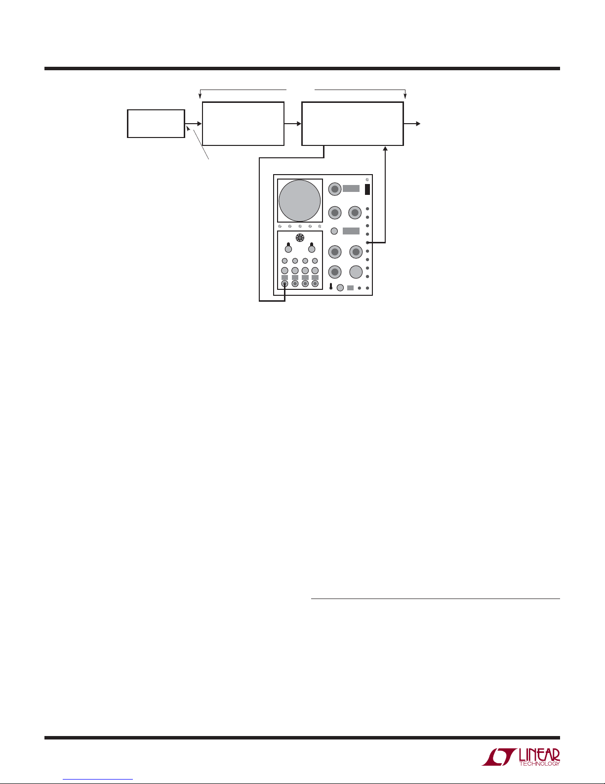
testing scheme includes a low noise pre-amplifier, filters
andapeak-to-peaknoisedetector.Thepre-amplifiers160nV
noise floor, enabling accurate measurement, requires
special design and layout techniques. A forward gain of
106permits readout by conventional instruments.
Figure 3’s detailed schematic reveals some considerations
required to achieve the 160nV noise floor. The references
DC potential is stripped by the 1300μF, 1.2k resistor
combination; AC content is fed to Q1. Q1-Q2, extraordi-
narily low noise J-FET’s, are DC stabilized by A1, with A2
providing a single-ended output. Resistive feedback from
A2 stabilizes the configuration at a gain of 10,000. A2’s
output is routed to amplifier-filter A3-A4 which provides
0.1Hz to 10Hz response at a gain of 100. A5-A8 comprise
a peak-to-peak noise detector read out by a DVM at a
scale factor of 1 volt/microvolt. The peak-to-peak noise
detectorprovideshigh accuracy measurement,eliminating
tedious interpretation of an oscilloscope display. Instanta-
neous noise value is supplied by the indicated output to a
monitoring oscilloscope. The 74C221 one-shot, triggered
by the oscilloscope sweep gate, resets the peak-to-peak
noise detector at the end of each oscilloscope 10-second
sweep.
Figure 1. LTC6655 Accuracy and Temperature Coefficient Are Characteristic of High Grade, Low Voltage References.
0.1Hz to 10Hz Noise, Particularly Noteworthy, Is Unequalled by Any Low Voltage Electronic Reference
Introduction
Frequently, voltage reference stability and noise define
measurement limits in instrumentation systems. In par-
ticular, reference noise often sets stable resolution limits.
Reference voltages have decreased with the continuing
drop in system power supply voltages, making reference
noise increasingly important. The compressed signal
processing range mandates a commensurate reduction
in reference noise to maintain resolution. Noise ultimately
translatesintoquantizationuncertainty in AtoDconverters,
introducing jitter in applications such as scales, inertial
navigation systems, infrared thermography, DVMs and
medical imaging apparatus. A new low voltage reference,
the LTC6655, has only 0.3ppm (775nV) noise at 2.5VOUT.
Figure 1 lists salient specifications in tabular form. Ac-
curacy and temperature coefficient are characteristic of
high grade, low voltage references. 0.1Hz to 10Hz noise,
particularly noteworthy, is unequalled by any low voltage
electronic reference.
Noise Measurement
Special techniques are required to verify the LTC6655’s ex-
tremely low noise. Figure 2’s approach appears innocently
straightforward but practical implementation represents a
highorderdifficultymeasurement.This0.1Hzto 10Hz noise
775 Nanovolt Noise Measurement for A Low Noise
Voltage Reference
Quantifying Silence
Jim Williams
LTC6655 Reference Tabular Specifications
SPECIFICATION LIMITS
Output Voltages 1.250, 2.048, 2.500, 3.000, 3.300, 4.096, 5.000
Initial Accuracy 0.025%, 0.05%
Temperature Coefficient 2ppm/°C, 5ppm/°C
0.1Hz to 10Hz Noise 0.775μV at VOUT = 2.500V, Peak-to-Peak Noise is within this Figure in 90% of 1000 Ten Second Measurement Intervals
Additional Characteristics 5ppm/Volt Line Regulation, 500mV Dropout, Shutdown Pin, ISUPPLY = 5mA, VIN = VO+ 0.5V to 13.2VMAX,
IOUT(SINK/SOURCE) = ±5mA, ISHORT Circuit = 15mA.
L, LT, LTC, LTM, Linear Technology and the Linear logo are registered trademarks of Linear
Technology Corporation. All other trademarks are the property of their respective owners.

Application Note 124
AN124-2
an124f
Numerous details contribute to the circuit’s performance.
The 1300μF capacitor, a highly specialized type, is selected
for leakage in accordance with the procedure given in
Appendix B. Further, it, and its associated low noise 1.2k
resistor, are fully shielded against pick-up. FETs Q1 and
Q2 differentially feed A2, forming a simple low noise op
amp. Feedback, provided by the 100k - 10Ω pair, sets
closed loop gain at 10,000. Although Q1 and Q2 have
extraordinarily low noise characteristics, their offset and
drift are uncontrolled. A1 corrects these deficiencies by
adjusting Q1’s channel current via Q3 to minimize the
Q1-Q2 input difference. Q1’s skewed drain values ensure
that A1 is able to capture the offset. A1 and Q3 supply
whatever current is required into Q1’s channel to force
offset within about 30μV. The FETs’ VGS can vary over
a 4:1 range. Because of this, they must be selected for
10% VGS matching. This matching allows A1 to capture
the offset without introducing significant noise. Q1 and
Q2 are thermally mated and lagged in epoxy at a time
constant much greater than A1’s DC stabilizing loop roll-
off, preventing offset instability and hunting. The entire
A1-Q1-Q2-A2 assembly and the reference under test are
completely enclosed within a shielded can.1The reference
is powered by a 9V battery to minimize noise and insure
freedom from ground loops.
Peak-to-peakdetectordesignconsiderationsincludeJ-FET’s
used as peak trapping diodes to obtain lower leakage than
afforded by conventional diodes. Diodes at the FET gates
clampreversevoltage,furtherminimizingleakage.2Thepeak
storage capacitors highly asymmetric charge-discharge
profile necessitates the low dielectric absorption polypro-
pelene capacitors specified.3Oscilloscope connections via
galvanically isolated links prevent ground loop induced
corruption. The oscilloscope input signal is supplied by an
isolated probe; the sweep gate output is interfaced with an
isolation pulse transformer. Details appear in Appendix C.
Noise Measurement Circuit Performance
Circuit performance must be characterized prior to mea-
suring LTC6655 noise. The pre-amplifier stage is verified
for >10Hz bandwidth by applying a 1μV step at its input
(reference disconnected) and monitoring A2’s output.
Figure4’s10ms risetimeindicates35Hz response, insuring
the entire 0.1Hz to 10Hz noise spectrum is supplied to the
succeeding filter stage.
Note 1. The pre-amplifier structure must be carefully prepared. See
Appendix A, “Mechanical and Layout Considerations”, for detail on pre-
amplifier construction.
Note 2. Diode connected J-FET’s superior leakage derives from their
extremely small area gate-channel junction. In general, J-FET’s leak a few
picoamperes (25°C) while common signal diodes (e.g. 1N4148) are about
1,000X worse (units of nanoamperes at 25°C).
Note 3. Teflon and polystyrene dielectrics are even better but the Real
World intrudes. Teflon is expensive and excessively large at 1μF. Analog
types mourn the imminent passing of the polystyrene era as the sole
manufacturer of polystyrene film has ceased production.
AN124 F02
SWEEP
GATE OUT
DC OUT
0V TO 1V = 0μVP-P TO
1μVP-P AT INPUT
VERTICAL
INPUT
≈700nV
NOISE
0.1Hz TO 10Hz
OSCILLOSCOPE
OUTPUT
A = 106
0.1Hz TO 10Hz FILTER AND
PEAK TO PEAK NOISE DETECTOR
0μV TO 1μV = 0V TO 1V, A = 100
LOW NOISE
AC PRE-AMP
EN, 0.1Hz TO 10Hz = 160nV
A = 10,000 RESET
LTC6655
2.5V REFERENCE
Figure 2. Conceptual 0.1Hz to 10Hz Noise Testing Scheme Includes Low Noise Pre-Amplifier, Filter and Peak to Peak Noise
Detector. Pre-Amplifier’s 160nV Noise Floor, Enabling Accurate Measurement, Requires Special Design and Layout Techniques

Application Note 124
AN124-3
an124f
+
–
100k100k
SHIELD
SHIELDED CAN
1N4697
10V
AC LINE GROUND
1300μF
9V
100k*
10Ω*
+
–
1k* 200Ω*
2k
450Ω* 900Ω*
15V
15V
–15V
–15V
1μF
1μF A1
LT1012
A2
LT1097
AN124 F03
– INPUT
Q1
5
* = 1% METAL FILM
** = 1% WIREWOUND, ULTRONIX105A
= 1N4148
= 2N4393
= 1/4 LTC202
SEE APPENDIX C FOR POWER, SHIELDING
AND GROUNDING SCHEME
= TANTALUM,WET SLUG
I
LEAK < 5nA
SEE TEXT/APPENDIX B
= POLYPROPELENE
A4 330μF OUTPUT CAPACITORS = <200nA LEAKAGE
AT 1VDC AT 25°C
Q1, Q2 = THERMALLY MATED
2SK369 (MATCH VGS 10%)
OR LSK389 DUAL
THERMALLY LAG
SEE TEXT
A = 104
LOW NOISE
PRE-AMP
REFERENCE
UNDER TEST
0.15μF
750Ω*
10k
–15V
Q3
2N2907
Q2 0.022μF
1μF
**1.2k
SD
LTC6655
2.5V
IN S
F
+
1μF
0.1μF
124k* 124k*
–
+
A3
LT1012
1M*
10k*
100Ω*330Ω*
IN OUT
ROOT-SUM-SQUARE
CORRECTION
SEE TEXT
330μF
16V
330μF
16V
+
+
330μF
16V
330μF
16V
+
–
A4
LT1012
0.1μF
0.1μF
10k
A = 100 AND
0.1Hz TO 10Hz FILTER
1μF
RST
+
–
A5
1/4 LT1058
–
+
A7
1/4 LT1058
1k
PEAK TO PEAK
NOISE DETECTOR
O TO 1V =
O TO 1μV
+ PEAK
4.7k
P
P
1μF
RST
15
0.1μF
+
–
A6
1/4 LT1058
–
+
A8
1/4 LT1058
1k
– PEAK
4.7k
10k
100k
100k
P
T
T
–
+
DVM
TO OSCILLOSCOPE INPUT
VIA ISOLATED PROBE,
1V/DIV = 1μV/DIV,
REFERRED TO INPUT,
SWEEP = 1s/DIV
FROM OSCILLOSCOPE
SWEEP GATE OUTPUT
VIA ISOLATION
PULSE TRANSFORMER
RESET PULSE
GENERATOR
0.22μF
C2 RC2
+15 +15
CLR2
+15
74C221
RST = Q2 +V
+15
A2
B2
10k
BAT-85
BAT-85
10k
+
+
0.005μF
–15
10k
0.005μF
Figure 3. Detailed Noise Test Circuitry. Thermally Lagged Q1-Q2 Low Noise J-FET Pair Is DC Stabilized by A1-Q3; A2 Delivers A = 10,000 Pre-Amplifier Output. A3-A4 form 0.1Hz to
10Hz ,A = 100, Bandpass Filter; Total Gain Referred to Pre-Amplifier Input Is 106. Peak to Peak Noise Detector, Reset by Monitoring Oscilloscope Sweep Gate, Supplies DVM Output

Application Note 124
AN124-4
an124f
Note 4. That’s right, a strip-chart recording. Stubborn, locally based
aberrants persist in their use of such archaic devices, forsaking more
modern alternatives. Technical advantage could account for this choice,
although deeply seated cultural bias may be indicated.
the LTC 6655’s expected 775nV noise figure. This term is
accounted for by placing Figure 3’s “root-sum-square cor-
rection”switchin theappropriateposition duringreference
testing. The resultant 2% gain attenuation first order cor-
rects LTC6655 output noise reading for the circuit’s 160nV
noise floor contribution. Figure 7, a strip-chart recording
of the peak-to-peak noise detector output over 6 minutes,
shows less than 160nV test circuit noise.4Resets occur
every 10 seconds. A 3V battery biases the input capacitor,
replacing the LTC6655 for this test.
Figure 8 is LTC6655 noise after the indicated 24-hour
dielectric absorption soak time. Noise is within 775nV
peak-to-peak in this 10 second sample window with
the root-sum-square correction enabled. The verified,
extremely low circuit noise floor makes it highly likely
this data is valid. In closing, it is worth mention that the
approach taken is applicable to measuring any 0.1Hz to
10Hz noise source, although the root-sum-square error
correction coefficient should be re-established for any
given noise level.
10ms/DIV
2mV/DIV
AN124 F04
Figure 4. Pre-Amplifier Rise Time Measures 10ms; Indicated
35Hz Bandwidth Ensures Entire 0.1Hz to 10Hz Noise Spectrum Is
Supplied to Succeeding Filter Stage
1s/DIV
E = 20V/DIV
D = 1V/DIV
C = 0.5V/DIV
B = 0.5V/DIV
A = 5mV/DIV
AN124 F05
Figure 5. Waveforms for Peak to Peak Noise Detector Include
A3 Input Noise Signal (Trace A), A7 (Trace B) Positive/A8
(Trace C) Negative Peak Detector Outputs and DVM Differential
Input (Trace D). Trace E’s Oscilloscope Supplied Reset Pulse
Lengthened for Photographic Clarity
1s/DIV
100nV/DIV
AN124 F06
Figure 6. Low Noise Circuit/Layout Techniques Yield 160nV
0.1Hz to 10Hz Noise Floor, Ensuring Accurate Measurement.
Photograph Taken at Figure 3’s Oscilloscope Output with 3V
Battery Replacing LTC6655 Reference. Noise Floor Adds ≈2%
Error to Expected LTC6655 Noise Figure Due to Root-Sum-Square
Noise Addition Characteristic; Correction is Implemented at
Figure 3’s A3
Figure 5 describes peak-to-peak noise detector operation.
Waveforms include A3’s input noise signal (Trace A), A7
(Trace B) positive/A8 (Trace C) negative peak detector
outputs and DVM differential input (Trace D). Trace E’s
oscilloscope supplied reset pulse has been lengthened
for photographic clarity.
Circuit noise floor is measured by replacing the LTC6655
with a 3V battery stack. Dielectric absorption effects in
the large input capacitor require a 24-hour settling period
before measurement. Figure 6, taken at the circuit’s oscil-
loscope output, shows 160nV 0.1Hz to 10Hz noise in a
10 second sample window. Because noise adds in root-
sum-square fashion, this represents about a 2% error in

Application Note 124
AN124-5
an124f
1 MIN AN124 F07
TIME
AMPLITUDE
100nV
0V
Figure 7. Peak to Peak Noise Detector Output Observed Over
6 Minutes Shows <160nV Test Circuit Noise. Resets Occur
Every 10 seconds. 3V Battery Biases Input Capacitor, Replacing
LTC6655 for This Test
1s/DIV
500nV/DIV
AN124 F08
Figure 8. LTC6655 0.1Hz to 10Hz Noise Measures 775nV in
10 Second Sample Time
REFERENCES
1. Morrison,Ralph, “Grounding andShieldingTechniques
in Instrumentation,” Wiley-Interscience, 1986.
2. Ott, Henry W., “Noise Reduction Techniques in Elec-
tronic Systems,” Wiley-Interscience, 1976.
3. LSK-389 Data Sheet, Linear Integrated Systems.
4. 2SK-369 Data Sheet, Toshiba.
5. LTC6655 Data Sheet, Linear Technology Corporation.
6. LT1533 Data Sheet, Linear Technology Corporation.
7. Williams, Jim, “Practical Circuitry for Measurement
and Control Problems,” Linear Technology Corpora-
tion, Application Note 61, August 1994.
8. Williams, Jim, “A Monolithic Switching Regulator with
100μV Output Noise,” Linear Technology Corporation,
Application Note 70, October 1997.
9. Williams, Jim and Owen, Todd, “Performance Verifica-
tion of Low Noise, Low Dropout Regulators,” Linear
Technology Corporation, Application Note 83, March
2000.
10. Williams, Jim, “Low Noise Varactor Biasing with
SwitchingRegulators,”LinearTechnology Corporation,
Application Note 85, August 2000, pages 4-6.
11. Williams, Jim, “Minimizing Switching Regulator Resi-
due in Linear Regulator Outputs,” Linear Technology
Corporation, Application Note 101, July 2005.
12. Williams, Jim, “Power Conversion, Measurement
and Pulse Circuits,” Linear Technology Corporation,
Application Note 113, August 2007.
13. Williams, Jim, “High Voltage, Low Noise, DC-DC Con-
verters,” Linear Technology Corporation, Application
Note 118, March 2008.
14. Tektronix, Inc., “Type 1A7 Plug-In Unit Operating and
Service Manual,” Tektronix, Inc., 1965.
15. Tektronix, Inc., “Type 1A7A Differential Amplifier Op-
erating and Service Manual,” Tektronix, Inc. 1968.
16. Tektronix,Inc.“Type7A22 Differential AmplifierOperat-
ing and Service Manual,” Tektronix, Inc., 1969.
17. Tektronix,Inc.,“AM502 Differential AmplifierOperating
and Service Manual,” Tektronix, Inc., 1973.

Application Note 124
AN124-6
an124f
Figure A1. Preamplifier Board Top (Figure A1A) and Bottom (A1B) Views. Board Top Includes Shielded Input Capacitor (Upper Left)
and Input Resistor (Upper Center Left). Stabilized JFET Input Amplifier Occupies Board Upper Center Right; Output Stage Adjoins
BNC Fitting. Reference Under Test Resides in Socket Below Input Capacitor. ±15 Power Enters Shielded Enclosure Via Banana Jacks
(Extreme Right). 9V Battery (Lower) Supplies Reference Under Test. Board Bottom’s Epoxy Filled Plastic Cup (A1B Center) Contains
JFETs, Provides Thermal Mating and Lag
APPENDIX A
Mechanical and Layout Considerations
The low noise X10,000 preamplifier, crucial to the noise
measurement, must be quite carefully prepared. Figure
A1 shows board layout. The board is enclosed within
a shielded can, visible in A1A. Additional shielding is
provided to the input capacitor and resistor (A1A left);
the resistor’s wirewound construction has low noise but
is particularly susceptible to stray fields. A1A also shows
the socketed LTC6655 reference under test (below the
large input capacitor shield) and the JFET input amplifier
associated components. Q3 (A1A upper right), a heat
source,is located awayfrom the JFET printed circuit lands,
preventing convection currents from introducing noise.
Additionally, the JFET’s arecontained within an epoxy filled
plasticcup (FigureA1B center),promoting thermal mating
and lag.1This thermal management of the FETs prevents
offset instability and hunting in A1’s stabilizing loop from
masquerading as low frequency noise. ±15V power enters
the enclosure via banana jacks; the reference is supplied
by a 9V battery (both visible in A1A). The A = 100 filter
andpeak-peak detector circuitryoccupiesa separateboard
outsidetheshielded can.Nospecial commentaryapplies to
this section although board leakage to the peak detecting
capacitors should be minimized with guard rings or flying
lead/Teflon stand-off construction.
Note 1. The plastic cup, supplied by Martinelli and Company, also
includes, at no charge, 10 ounces of apple juice.
Figure A1A. Figure A1B.

Application Note 124
AN124-7
an124f
AN124 FB01
HP-419A MICROVOLT METER
+–
1300μF/30V
VISHAY
XTV138M030P0A
WET SLUG TANTALUM
TEST SEQUENCE
1. TURN OFF MICROVOLT METER
2. CONNECT 3V BATTERY STACK
3. WAIT 24 HOURS
4. TURN ON MICROVOLT METER
5. READ CAPACITOR LEAKAGE, 1nA = 1μV
1.5V
3V
AA
CELLS
1.5V
1k
hp
+–
Figure B1. Pre-Amplifier Input Capacitor Selected for <5nA Leakage to Minimize DC Error and Capacitor
Introduced Noise. Capacitor Dielectric Absorption Requires 24 Hour Charge Time to Insure Meaningful
Measurement. Highest Grade Wet Slug Tantalum Capacitors are Required to Pass This Test
APPENDIX B
Input Capacitor Selection Procedure
The input capacitor, a highly specialized type, must be
selected for leakage. If this is not done, resultant errors
can saturate the input pre-amplifier or introduce noise.
The highest grade wet slug 200°C rated tantalum capaci-
tors are utilized. The capacitor operates at a small frac-
tion of its rated voltage at room temperature, resulting
in much lower leakage than its specification indicates.
The capacitor’s dielectric absorption requires a 24-hour
chargetime toinsure meaningfulmeasurement. Capacitor
leakage is determined by following the 5-step procedure
given in the figure. Yield to required 5-nanoampere leak-
age exceeds 90%.1
Note 1. This high yield is most welcome because the specified capacitors
are spectacularly priced at almost $400.00. There may be a more palatable
alternative. Selected commercial grade aluminum electrolytics can
approach the required DC leakage although their aperiodic noise bursts
(mechanism not understood; reader comments invited) are a concern.

Application Note 124
AN124-8
an124f
–
+
DVM
PEAK TO PEAK
RESET
SWEEP RESET
VERTICAL
INPUT
9V
BATTERY
REFERENCE
UNDER TEST
A = 10,000
PRE-AMP
PULSE ISOLATION
TRANSFORMER/
COAXIAL CAPACITOR
LOW SHUNT
CAPACITANCE ISOLATION
TRANSFORMER
(LOCATE ≥3 FEET
FROM SHIELDED CAN)
110VAC
LINE INPUT
TOPAZ, 0111T35S
INSTRUMENT
GRADE ±15V
POWER SUPPLY
+15
DEERFIELD LAB 185,
HEWLETT PACKARD
10240B
HEWLETT PACKARD,
6111A,
PHILBRICK RESEARCHES
6033, PR-300
TEKTRONIX A6909,
TEKTRONIX A6902B,
SIGNAL ACQUISITION
TECHNOLOGIES SL-10
A = 100
FILTER AND
PEAK TO PEAK
DETECTOR
ISOLATED
PROBE
–15
AN124 FC1
SHIELDED CAN
RF
FEEDTHROUGHS
OSCILLOSCOPE
CIRCUIT
COMMON
= CIRCUIT COMMON
= AC LINE GROUND
CURRENT
MONITOR
LOOP
Figure C1. Power/Grounding/Shielding Scheme for Low Noise Measurement Minimizes AC Line Originated Interference
and Mixing of Circuit Return and AC Line Ground Current. No Current Should Flow in Current Monitor Loop
APPENDIX C
Power, Grounding and Shielding Considerations
Figure 3’s circuit requires great care in power distribution,
grounding and shielding to achieve the reported results.
Figure C1 depicts an appropriate scheme. A low shunt ca-
pacitance line isolation transformer powers an instrument
grade ±15V supply, furnishing clean, low noise power. The
pre-amplifier’s shielded can is tied to the 110V AC ground
terminal, directing pick-up to earth ground. Filter/peak-to-
peak detector oscilloscope connections are made via an
isolatedprobeand a pulseisolationtransformer, precluding
errorinducing groundloops.1The indicated loop, included
toverify no currentflow betweencircuitcommonand earth
ground, is monitored with a current probe. Figures C2 and
C3, both optional, show battery powered supplies which
replace the line isolation transformer and instrumentation
grade power supplies. C2 uses linear regulators to fur-
nish low noise ±15V. Because the batteries float, positive
regulators suffice for both positive and negative rails. In
C3, a single battery stack supplies an extremely low noise
DC-DC converter to furnish positive and negative rails via
low noise discrete linear regulators.2Both of these battery
supplied approaches are economical compared to the AC
line powered version but require battery maintenance.
The indicated commercial products accompanying
Figure C1’sblocks representtypical applicable units which
have been found to satisfy requirements. Other types
may be employed but should be verified for necessary
performance.
Note 1. An acceptable alternative to the isolated probe is monitoring
Figure 3’s A4 output current into a grounded 1k resistor with a DC
stabilized current probe (e.g. Tektronix P6042, AM503). The resultant
isolated 1V/μV oscilloscope presentation requires 10Hz lowpass filtering
(see Appendix D) due to inherent current probe noise.
Note 2. References 6 and 8 detail the specialized DC-DC converter used.

Application Note 124
AN124-9
an124f
Figure C2. LT1761 Regulators form ±15V, Low Noise Power Supply. Isolated Battery Packs Permit Positive
Regulator to Supply Negative Output and Eliminate Possible AC Line Referred Ground Loops
12 Size D
ALKALINE
1.5V CELLS
EACH PACK
LT1761
SD B
FB
IN OUT
+18
+15
0.1μF
13.7k*
AN124 FC2
* = 1% METAL FILM RESISTOR
+
10μF10μF
10μF
+
1.21k*
LT1761
SD B
FB
IN OUT
0.1μF
13.7k*
+
1.21k*
–15
10μF
+

Application Note 124
AN124-10
an124f
+
VIN
CT
6V
3300pF
RVSL
GND FB RT
RCSL DUTY
LT1533
PGND
COL A
COL B
15k
4.7μF 15k
32
151689
14 13 12
6
5
2
3
4
7
12
10
9
5
6V
18k L1
T1
100μF
4.7μF
+
+
100μF
AN124 FC3
+
+ +
L1: 22nH INDUCTOR. COILCRAFT B-07T TYPICAL,
PC TRACE, OR FERRITE BEAD
L2, L3: PULSE ENGINEERING. PE92100
T1: COILTRONICS CTX-02-13664-X1
: 1N4148
* = 1% METAL FILM
10k
43k
5V
L1
25μH
–15VOUT
15VOUT
OUT
COMMON
L2
25μH
10k*
4.99k*
5k
8
4
6V BATTERY
4x 1.5V
ALKALINE
D CELL
LT 1 0 1 0
+
–
1/2 LT1013
1μF
47μF
0.1μF
47μF
0.1μF
10V
OUT
IN
19V UNREGULATED
–19V UNREGULATED
LT 1 0 2 1
10k*
10k*
LT1010
+
–
1/2 LT1013
Figure C3. A Low Noise, Bipolar, Floating Output Converter. Grounding LT1533 “DUTY” Pin and Biasing FB Puts Regulator into 50%
Duty Cycle Mode. LT1533’s Controlled Transition Times Permit <100μV Broadband Output Noise; Discrete Linear Regulators Maintain
Low Noise, Provide Regulation

Application Note 124
AN124-11
an124f
Information furnished by Linear Technology Corporation is believed to be accurate and reliable.
However, no responsibility is assumed for its use. Linear Technology Corporation makes no representa-
tion that the interconnection of its circuits as described herein will not infringe on existing patent rights.
MANUFACTURER MODEL NUMBER MODIFICATION
Tektronix 1A7 Parallel C370A with 1μF
Tektronix 1A7A Parallel C445A with 1μF
Tektronix 7A22 Parallel C426H with 3μF
Tektronix AM502 Parallel C449 with 3μF
Figure D2. Modification Information for Various Tektronix Low
Level Oscilloscope Plug-In’s and Amplifiers Permits 10Hz High
Frequency Filter Operation in 100Hz Panel Switch Position. All
Cases Utilize 100V, Mylar Capacitors
INSTRUMENT
TYPE MANUFACTURER
MODEL
NUMBER
–3dB
BANDWIDTH
MAXIMUM
SENSITIVITY/GAIN AVAILABILITY COMMENTS
Differential Amplifier Tektronix 1A7/1A7A 1MHz 10μV/DIV Secondary Market Requires 500 Series Mainframe,
Settable Bandstops
Differential Amplifier Tektronix 7A22 1MHz 10μV/DIV Secondary Market Requires 7000 Series Mainframe,
Settable Bandstops
Differential Amplifier Tektronix 5A22 1MHz 10μV/DIV Secondary Market Requires 5000 Series Mainframe,
Settable Bandstops
Differential Amplifier Tektronix ADA-400A 1MHz 10μV/DIV Current Production Stand-Alone with Optional Power
Supply, Settable Bandstops
Differential Amplifier Preamble 1822 10MHz Gain = 1000 Current Production Stand-Alone, Settable Bandstops
Differential Amplifier Stanford
Research
Systems
SR-560 1MHz Gain = 50000 Current Production Stand-Alone, Settable Bandstops,
Battery or Line Operation
Differential Amplifier Tektronix AM-502 1MHz Gain = 100000 Secondary Market Requires TM-500 Series Power
Supply, Settable Bandstops
Figure D1. Some Useful High Sensitivity, Low Noise Amplifiers. Trade-Offs Include Bandwidth, Sensitivity and Availability
APPENDIX D
High Sensitivity, Low Noise Amplifiers
Figure D1 lists some useful low level amplifiers for setting
up and troubleshooting the texts’ circuit. The table lists
bothoscilloscopeplug-in amplifiers andstand-alonetypes.
Two major restrictions apply. The filters in these units
are single-pole types resulting in somewhat pessimistic
bandwidth cut-offs. Additionally, the amplifiers listed do
not include 10Hz lowpass frequency filters, although
they are easily modified to provide this capability. Figure
D2 lists four amplifiers with the necessary modification
information.1
Note 1. See References 14-17.

Application Note 124
AN124-12
an124f
Linear Technology Corporation
1630 McCarthy Blvd., Milpitas, CA 95035-7417
(408) 432-1900 ●FAX: (408) 434-0507 ● www.linear.com
© LINEAR TECHNOLOGY CORPORATION 2009
LT 0709 • PRINTED IN USA
1s/DIV
500nV/DIV
AN124 QT


